


I. INTRODUCTION
In recent years, as the demand of portable systems have increased, low profile systems have drawn much interest of researchers. In making such low profile communication systems, the size of the antenna is critical. To the growing demand of MMIC (monolithic microwave integrated circuits) compatible antennas – patch antennas are a good solution. To integrate these antennas in MMIC for wireless communication applications the size of these microstrip antennas should be as small as possible without compromising on their performance. Therefore, several kinds of miniaturization techniques, such as use of high dielectric substrates [Reference Lo and Hwang1], applying resistive or reactive loading [Reference Sinati2], increasing the electrical length of the antenna by optimizing its shape [Reference Wang and Lancaster3], use of notches and short circuits on the patch antenna [Reference Waterhouse4], and use of magnetic substrates have been proposed and applied to microstrip patch antennas [Reference Anguera, Boada, Puente, Borja and Soler5]. Techniques to achieve dual-band operation of microstrip antennas are also available in [Reference Kordzadeh and HojatKashani6–Reference Zhong and Cui9]. In addition to this, dual-band operation with slots and stacked structure are available in [Reference Wu10–Reference Lin and Wong13] and [Reference Anguera, Puente, Borja, Delbene and Soler14, Reference Zhou, Chen and Volakis15], respectively.
The application of fractal geometry to conventional patch antenna structures modifies the shape of the antennas in order to increase its effective electrical length at the same time reducing their overall geometrical size. Since fractal geometries have two main features in common, space-filling and self-similar properties, fractal shape antenna elements present various advantages such as wide bandwidth, multiband [Reference Puente, Romeu, Pous and Cardma16] and reduced antenna size [Reference Malik and Kartikeyan17] among others. Sierpinski fractal geometry exhibits well-known features that have been used to construct miniaturized radiating patches either monopole or dipole antennas. In the present work, a complementary Sierpinski gasket fractal geometry has been applied to an equilateral triangular microstrip patch antennas to reduce its overall size, and the effectiveness of this technique is verified through experimental investigations. It is found that as the iteration number increases, the resonance frequencies become lower than those of the zero iteration, which represents a conventional equilateral triangular patch.
Today, the most wide spread protocols are IEEE 802.16a WiMAX, which utilizes the 3.5 GHz band and IEEE 82.11a WLAN, which employs the 5.8 GHz band. For system flexibility and feasibility, the antennas that have the ability to operate at both the specified frequency bands are highly desired. An electromagnetic coupled stacked structure to operate at two different frequencies (3.5 GHz WiMAX and 5.8 GHz wireless LAN) has been designed for dual-band wireless applications.
II. ANTENNA GEOMETRY AND SIMULATION
The antenna configuration of proposed stacked resonator structure is shown in Fig. 1. Both resonators are equilateral triangles modified with 2nd iteration Sierpinski gasket fractal. Steps to generate complementary Sierpinski gasket fractal are demonstrated in Fig. 1(b). The substrate used has relative permittivity ɛr = 3.38 and thickness 1.524 mm (60 mil). A layout in Fig. 1(c) shows relative position of patches and orientation. The size of the substrate used is 25 mm × 35 mm. The resonant frequencies of a simple equilateral triangular patch without any degree of Sierpinski gasket fractal is calculated using [Reference Dahele18].
 $$f_{m\comma n\comma 1}=\displaystyle{{2c} \over {3a\lpar \varepsilon _r \rpar ^{1/2} }}\lpar m^2+mn+n^2 \rpar ^{1/2}\comma \;$$
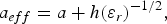 $$a_{eff}=a+h\lpar \varepsilon _r \rpar ^{ - 1/2}\comma \;$$
 $$\varepsilon _{eff}=\displaystyle{1 \over 2}\lpar \varepsilon _r+1\rpar +\displaystyle{1 \over 4}\lpar \varepsilon _r - 1\rpar \left({1+\displaystyle{{12h} \over a}} \right)^{ - 1/2}\comma \;$$
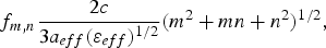 $$f_{m\comma n} \displaystyle{{2c} \over {3a_{eff} \lpar \varepsilon _{eff} \rpar ^{1/2} }}\lpar m^2+mn+n^2 \rpar ^{1/2}\comma \;$$
where a is the length of equilateral triangular patch; h the thickness of substrate; ɛ r the relative dielectric constant; c the velocity of light; and TMm,n is the resonant fundamental mode. Here m = 0, n = 1.

Fig. 1. (a) Stack antenna configuration. (b) Steps for generation of complementary patch. (c) Top view of three layers separately (black portion represents metallic part).
The calculated side length of equilateral triangular patch from above equations (1–4) was taken as starting value. During simulation it was observed that with increase in fractal iteration count the side length for both patch decreased for operation in same band. For 2nd degree fractal bottom patch has side length a = 13.8 mm and the upper patch is of side length b = 30 mm. proximity coupled feed has been used to excite the lower patch and upper patch is electromagnetically coupled to the lower patch. The centroids of lower and upper patchs are 18.98 and 19.32 mm, respectively, above the lower edge of substrate along Y-axis at the tuned positions, respectively. The width of feed line is set to achieve line impedance of 50 Ω. The length of feed line is 22.5 mm and the distance (Y1) between upper edge of feed line and centroid of lower patch is 3.52 mm.
A) Return loss and Smith chart
The proposed antenna was designed and simulated in finite integration technique based CST MWS V9. To simulate the antenna Transient solver was chosen with hexahedral mesh cell Port impedance was adjusted to obtain 50 Ω.
The simulated return loss result and smith chart plot are shown in Fig. 2. The antenna covers the WLAN standards IEEE 802.16a (3.5 GHz band) and IEEE 82.11a (5.8 GHz band) with adequate bandwidth of 130 and 140 MHz, respectively. Two distinct lopes in the Smith chart corresponds two resonances. After fabrication, the return loss of the antenna was tested on HP Network Analyzer and the fabricated antenna's result was found to be in good agreement with the simulated result.

Fig. 2. The simulated (a) |S 1, 1| dB and (b) Smith chart.
B) Variation of return loss with parametric analysis of design parameter
A detailed parametric analysis for the proposed antenna structure was done. From Fig. 3(a), it can be observed that changing the side length (“a”) of lower patch has prominent effect on the higher 5.8 GHz band. The resonant frequency decreases as the side length of lower patch increase in 5.8 GHz band, which is consistent with inverse law between length and resonant frequency. Changing the side length (“a”) has no effect on the resonance frequency in 3.5 GHz band except very little change in magnitude of return loss. From Fig. 3(b), one can see that the variation of side length of upper patch (“b”) affects 3.5 GHz band resonance, which is also consistent with theory. Shifting of return loss level upward was observed for both the cases, which may be due to the change in input impedance.

Fig. 3. Effects of varying side lengths of (a) lower patch and (b) upper patch on the return loss pattern.
Figure 4 shows the effect of moving the patches about their tuned position, one at a time on the magnitude of return loss and resonant frequency while keeping other parameters unaltered. In Fig. 4(a), effect of moving lower patch about its tuned position magnitude of return loss level at higher resonance decreases but no change/shifting regarding resonant frequencies for both bands are observed. As distance (between patch and feed line along Y-axis) increased in either direction, less power coupling occurs between feed line and patch. In Fig. 4(b), both the resonances are affected while moving the upper patch about its tuned position. Prominent change in both return loss level and bandwidth (both decreases) is observed at lower resonance. Little shifting of resonance at higher band is observed but no change in the impedance bandwidth was observed. These changes may be due to the electromagnetic coupling between patches. As upper patch is moved away from its tuned position, less power coupling occurs resulting shifting of return loss level upward at lower resonance.

Fig. 4. Effect of moving (a) lower patch and (b) upper patch about their tuned position on the return loss pattern (while moving one patch, other kept fixed at its tuned position).
C) Current distribution
The current distributions for the lower and upper patches at the 3.5 and 5.8 GHz bands are shown in Figs 5 and 6. The surface current densities on both the patches are shown for both 3.5 and 5.8 GHz frequencies. From the current density values shown against each patch, it can be concluded that at higher resonance, i.e. 5.8 GHz frequency the current density on smaller patch is more compared with that of bigger patch, which means that it is responsible for higher resonance.

Fig. 5. Current distributions on (a) lower patch and (b) upper patch at 3.5 GHz bands.

Fig. 6. Current distributions on (a) lower patch and (b) upper patch at 5.8 GHz bands.
III. FABRICATION AND MEASUREMENT
The simulated antenna was fabricated using photolithography process; thereafter its radiation pattern (E-field and H-field power pattern) was measured. The return loss was measured with HP Network Analyzer (HP 8720B) and the radiation performance was measured in the anechoic chamber.
The transmitter antenna was given 15 dBm power from the RF power generator, and the distance between the transmitter and the receiver was kept at 1.5 m. Gain was calculated using the substitution method with the help of the standard gain horn antenna (reference antenna) working in the range of 0.9–8 GHz. Figure 7(a) shows the fabricated antenna. The measured return loss and Smith chart are shown in Figs 7(b) and 7(c), respectively.

Fig. 7. (a) The fabricated antenna (b) measured |S 1, 1| dB and (c) Smith chart.
Figures 8 and 9 show the simulated and measured radiation patterns of the antenna in both the E- and the H-plane at the frequency bands of 3.5 and 5.8 GHz. The simulated and measured radiation patterns for E-plane at both 3.5 and 5.8 GHz bands are in close agreement. The measured radiation pattern in H-plane at both 3.5 and 5.8 GHz bands are slightly tilted compared with that of the simulated patterns. This may be due to the alignment error. Possible reasons for these disagreements between simulated and measured results may due to the possible presence of interference and noise.

Fig. 8. Simulated and measured (a) E-plane radiation pattern and (b) H-plane radiation pattern at 3.5 GHz.

Fig. 9. Simulated and measured (a) E-plane radiation pattern and (b) H-plane radiation pattern at 5.8 GHz.
The simulated and measured gain curves are given for the 3.5 and 5.8 GHz bands in Fig. 10. At both 3.5 and 5.8 GHz bands the maximum power was received by the antenna in the broadside direction. Consequently, gain measurements are done for the two-frequency bands in the directions of their respective maxima using the substitution/gain-transfer technique with the help of a standard horn antenna with calibrated gain. Less than 0.7 dB of difference in the simulated and measured gains was observed for both the band, which can be attributed to fabrication and measurement errors. Connectors and other devices such as cables also cause signal loss. This is due to a combination of the impedance mismatch between one cable/connector and the connector/antenna. The feeding line was designed for 50 Ω impedance, but minor design variations can cause impedance mismatch, hence losses. It affects the overall gain and return loss of the antenna. Also the spurious radiation at the connector/antenna junction can affect the radiation pattern of the antenna.

Fig. 10. Simulated and measured gains at (a) 3.5 GHz and (b) at 5.8 GHz bands.
IV. CONCLUSIONS
A stacked structure of complementary Sierpinski gasket fractal geometry applied to an equilateral triangular microstrip patch antenna was designed with fractal shapes being excoriated from both the radiating patch surfaces. The fractal modifications (2nd degree Sierpinski gasket) resulted in longer current paths on the patches, which led to size reduction. For a simple equilateral triangular patch having zero iteration of Sierpinski gasket fractal, the side length of resonating patch (for m = 0, n = 1) are about 31.08 mm and about 18.7 mm for 3.5 and 5.8 GHz, respectively. The side lengths of resonating equilateral triangular patch with 2nd iteration Sierpinski gasket fractal are 30 and 13.8 mm for 3.5 and 5.8 GHz, respectively. A size reduction of about 3.5 and 26% for 3.5 band and 5.8 GHz band, respectively, was observed in the present study. In addition, the stack structures make possible simultaneous dual-band performance of the antenna. The return loss of the fabricated antenna indicates a −10 dB impedance bandwidth of 100 MHz at the 3.5 GHz band and an impedance bandwidth of 150 MHz at the 5.8 GHz band. With suitable scaling, the proposed structure may find successful application in the millimeter wave range also.
 Jagannath Malik received his integrated dual degree in Electronics and Wireless Communication from Indian Institute of Technology, Roorkee, India. His area of research includes antenna, soft computing techniques and millimeter wave designs. He has authored a number of research articles on artificial neural networks, antennas and one book chapter on soft computing.
 Parth C. Kalaria is currently pursuing his master's degree from Indian Institute of Technology, Roorkee, India in RF and microwave. He received his Bachelors of Technology from Nirma University, Ahmedabad, India in Electronics and Communication Engineering. His areas of expertise include antenna, UWB techniques, microwave circuits and millimeter wave source design. Currently he is working toward high power gyrotron design for fusion reactors.
 M. V. Kartikeyan was born in Nellore (Andhra Pradesh), India, in 1961. He received the M.Sc. and Ph.D. degrees in 1985 and 1992 in physics and electronics engineering, respectively, from the Banaras Hindu University, India. Dr. Kartikeyan is the recipient of a Hildegard-Maier Research Fellowship for Electrical Sciences of the Alexander von Humboldt Foundation and the Alexander von Humboldt Research Fellowship for long-term cooperation and worked at the Institut für Hochleistungsimpuls- und Mikrowellentechnik, Karlsruhe Institute of Technology, Karlsruhe, Germany. He joined the Department of Electronics and Computer Engineering, Indian Institute of Technology, Roorkee, India, in 2003 as an Associate Professor and presently he is working as a Full-Professor. His research interests include millimeter wave engineering (electron cyclotron masers and other high power devices and components), microstrip antennas for communications, computational electromagnetics, microwave integrated circuits, and RF & microwave design with soft computing techniques. Dr. Kartikeyan is a Fellow of the Institution of Electronics and Telecommunications Engineers (IETE), Fellow of the Institution of Engineers (IE), India and Senior Member of IEEE.


