I. INTRODUCTION
With the introduction of new mobile applications, new operating bands are assisted. In other words, due to capacity problems in the conventional base-station systems such as the GSM900 wireless communication system, additional licenses for multi-bands operating frequency such as DCS1800 (Digital Cellular system), PCS1900 (Personal Communications Service), and UMTS2100 (Universal Mobile Telecommunication system) are utilized to overcome these problems. Because of this fact, much work has been devoted to increase the bandwidth or to obtain dual-frequency characteristics of the microstrip antennas. Several techniques, such as using two adjacent patch radiators operated at different frequencies [Reference Amiri and Forooraghi1], reactive loading [Reference Nakano and Vichien2], aperture-stacked patches (ASPs), [Reference Targonski, Waterhouse and Pozar3] and others have been reported in the last few years to obtain a much larger bandwidth or dual-band behavior.
In the last decade, many techniques have been reported in order to investigate dual-band dual-polarized antennas that suit the mobile base station. In [Reference Oh, Kim and Choi4, Reference Nikmehr and Moradi5], a dual-band dual-polarized ASP antenna with double-sided notches operating at GSM900, DCS1800, and UMTS2100 band operations was introduced. The dual-band operation behavior was obtained by introducing a reactive loading where an inset or a notch is cut on the radiating patch. The isolation between the two ports was 30 dB over its operating bands. However, this structure has a high back radiation at the UMTS2100 operating band where the front-to-back ratio (FBR) approaches 4.1 dB.
Caso et al. [Reference Caso, Serra, Pino-Rodriguez, Nepa and Manara6] introduced dual-polarized wideband-stacked patches fed through a slot-coupling technique [Reference Caso, Serra, Pino-Rodriguez, Nepa and Manara7], where two stacked resonant patches are coupled to the feeding line through a square ring slot. The antenna operates in the GSM 1800–1900 band (1710–1910 MHz), the UMTS2100 band (1920–2170 MHz), the ISM band (2400–2484 MHz), and the UMTS 3 G band (2500–2690 MHz). The antenna element was placed in an array of 2 × 1 with 22 dB isolation between the ports in the whole frequency band of interest. Therefore, the antenna has a slightly poor isolation between the two operating ports. The antenna element gain is between 6 and 7 dBi in the entire band of interest.
In [Reference Kaboli, Mirtaheri and Abrishamian8], a dual-band dual-linear slant polarized ASP operated at the GSM900 band has been published. This antenna supports only the GSM900 band. The structure consists of a reflector; a U-shaped microstrip feed line, a cross-slot, a patch, and a director. The polarization isolation at ±45° is >30 dB for a dual-linear polarization over its operating band. Kaboli et al. [Reference Kaboli, Abrishamian, Mirtaheri and Aboutorab9] introduced the extension to the work of [Reference Kaboli, Mirtaheri and Abrishamian8]. The XX-polar antenna operates at the GSM900 and (the DCS/UMTS) and is placed over the director of the GSM band. A quad-port antenna is used for achieving both the dual-band and the dual-polarization operation. Two ports are used for the GSM900 band and the other two ports are used to excite the second (the DCS/UMTS) band. The antenna exhibits dual-linear polarizations at ±45° slanted with an isolation of more than 30 dB when the four ports are simultaneously excited. The average gains are about 9.3–10.2 and 8.6–10 dBi in the lower and upper bands, respectively. The total length, width, and height of the antenna are 260 × 274 × 115 mm3, respectively.
In this paper, a new configuration of the dual-band dual-polarized microstrip slot antenna used in mobile base stations is proposed. The proposed antenna operates at the 870–960 MHz (GSM850/GSM900) and the 1710–2170 MHz (DCS1800/PCS1900/UMTS2100) bands which are needed to operate both the 2G and the 3G generations of mobile phone communication systems. The antenna exhibits dual-linear polarization at 0 and a 90° linear polarization with an isolation of more than 30 dB when the two ports are simultaneously excited. The FBR exceeds 15 dB at the lower band (GSM850/GSM900), and ranges from 16 to 25 dB at the upper bands (DCS1800, PCS1900, and UMTS2100). A dual orthogonal fork feed is used for transmitting and receiving operations. The antenna is designed and fabricated using a combination of FR4 dielectric and foam/air layers in order to obtain a low-cost structure. Furthermore, it is relatively compact and has a simple structure, in comparison with similar works conducted in this area.
II. THEORY OF OPERATION FOR SLOT ANTENNA AND ANTENNA PARAMETRIC STUDY
A) Theory of operation
The proposed antenna emulates a slot radiator mounted on an artificial magnetic conductor (AMC). The AMC is emulated using two reflectors of quarter wavelength spacing apart from the slot radiator at the center frequency of the lower and the upper bands. Figure 1 shows the rectangular slot with its coordinate system. The theory behind the proposed antenna is the emulation of a magnetic conductor beneath the slot radiator. The AMC surfaces have two important properties that led to a wide range of microwave circuit applications. First, the AMC surface has a forbidden frequency band over which surface waves and currents cannot propagate [Reference Sievenpiper, Zhang, Broas, Alexopolous and Yablonovitch10]. Second, the AMC surface has very high surface impedance within a specific limited frequency range, where the tangential magnetic field is small, even with a large electric field along the surface [Reference Sievenpiper, Zhang, Broas, Alexopolous and Yablonovitch10, Reference Yang, Ma, Qian and Itoh11]. Therefore, an AMC surface can have a reflection coefficient of +1 (in-phase reflection). Generally, the reflection phase is defined as the phase of the reflected electric field, which is normalized to the phase of the incident electric field at the reflecting surface. In practice, the reflection phase of an AMC surface varies continuously from +180 to −180 relative to the frequency, and crosses zero at just one frequency (for one resonant mode). The useful bandwidth of an AMC is generally defined as +90° to −90° on either side of the central frequency. The fact that the slot supports the radiation of an infinite number of modes encourages us to enhance the radiation of the modes that support the desired operating frequencies by exciting those modes.

Fig. 1. Rectangular aperture on an infinite ground plane.
The enhancement is achieved by placing reflectors with gradually increasing size at distances of quarter wavelengths with respect to its operating frequency. In other words, a small reflector at a quarter wavelength of the higher frequency is set first, and then a larger reflector at a larger distance (quarter wavelength at the lower operating frequency) is also set. By this configuration, an AMC at the two operating bands is achieved. The field emitted from the slot travels a distance of half-wavelength during its front and back propagation toward the reflector. This results in a 180° phase shift followed by another 180° phase shift due to the conductor-reflecting surface, which indeed results in a 360° phase shift that corresponds to the effect of the magnetic wall.
Assuming an excitation for the TE m0 modes, the only magnetic field component that exists is the x-directed magnetic field component:
 $$\mathop H\limits^{\to} = H_{x0} {\rm Sin}\left({\displaystyle{{m\pi x} \over a}} \right)\hat x\quad \left\{{\matrix{ {0\lt x\lt a\comma \; } \cr {0\lt y\lt b.} \cr } } \right.$$
According to the field equivalence principle [Reference Stutzman and Thiele12], we assume a magnetic wall at z = 0 where the equivalent electric current density is given by  $\vec{J}_{se}=\hat n \times \vec{H}$. On applying the image theory, the equivalent magnetic surface current vanishes while; the equivalent electric current is [Reference Stutzman and Thiele12]:
 $$\vec{J}_S=\left\{{\matrix{ { 2 H_{x } \,\hat y= 2 H_{x 0 }\, {\rm sin}\left({\displaystyle{{m\pi x} \over a}} \right)\hat y} \cr 0 \cr } } \right.\quad \matrix{ {\left\{{\matrix{ {0\lt x\lt a\comma \; } \cr {0\lt y\lt b\comma \; } \cr } } \right.} \cr {{\rm elsewhere} .} \cr }$$
The far field of the electric field could be approximated as:
 $$E^{far}=- j\omega \left[{A_\theta \hat \theta+A_\varphi \hat \varphi } \right]\comma \;$$
where, the magnetic vector potential  $\vec{A}$ is given by
 $$\mathop A\limits^{\to} \approx \displaystyle{{\mu e^{ - jkr} } \over {4\pi r}}\int\!\int_s {\vec{J}_s e^{jk\left({x^{\prime}\sin \theta \cos \varphi+\sin \theta \sin \varphi } \right)} } ds^{\prime}\comma \;$$
 $\hat \theta$ and
  $\hat \phi$ are the spherical coordinate components.
By some mathematical manipulation, the electric field could be written as
 $$E_\theta \cong - \displaystyle{{jke^{ - jkr} } \over {4\pi r}}\eta P_\theta\comma \;$$
 $$E_\varphi \cong \,\displaystyle{{jke^{ - jkr} } \over {4\pi r}}\eta P_\varphi\comma \;$$
where
 $$P{}_\theta=\left({2H_{x0} \cos \lpar \theta \rpar \cos \lpar \varphi \rpar } \right)I_x^H\comma \;$$
 $$P{}_\varphi=\left({ - 2H_{x0} \sin \lpar \varphi \rpar } \right)I_x^H.$$
The integral I xH in equations (6) and (7) is written as
 $$I_x^H=\vint\limits_0^b {\vint\limits_0^a {\sin \left({\displaystyle{{m\pi x^{\prime}} \over a}} \right)} } \mathop e\nolimits^{ja_0 x^{\prime}} \mathop e\nolimits^{jb_0 y^{\prime}} dx^{\prime}dy^{\prime}\comma \;$$
where a 0 = k sin θ cos φ and b 0 = k sin θ sin φ.
The integral in equation (8) could be simplified to the following form:
 $$I_x^H=- \left({\displaystyle{{m\pi b} \over a}} \right)\left[{\displaystyle{{1 \pm e^{jYa} } \over {\left({\left(Y \right)^2 - \left({\displaystyle{{m\pi } \over a}} \right)^2 } \right)}}} \right]\displaystyle{{\sin X} \over X}\mathop e\nolimits^{jX}\comma \;$$
where
 $$\eqalign{& X=\lpar bk\sin \theta \sin \varphi \rpar /2\semicolon \; \cr & Y=\lpar k\sin \theta \cos \varphi \rpar .}$$
The +ve sign in equation (9) is used for the odd numbers of m while the –ve sign is used for the even numbers of m.
The previous analytical equation is compared with a simulated rectangular slot antenna of length a = 107 mm and width b = 11 mm etched on the ground plane and a fork-shaped feed line is placed on the opposite side of the FR4 substrate with ε r = 4.5, substrate height (h) = 1.5 mm, and loss tangent (tan δ) = 0.025. The far-field pattern of the slot antenna using analytical solution compared to the simulation one is shown in Fig. 2.
Fig. 2. (a) Analytical and simulation far-field patterns at f = 915 MHz, (b) analytical and simulation far-field patterns at f = 1710 MHz.
B) Antenna parametric study
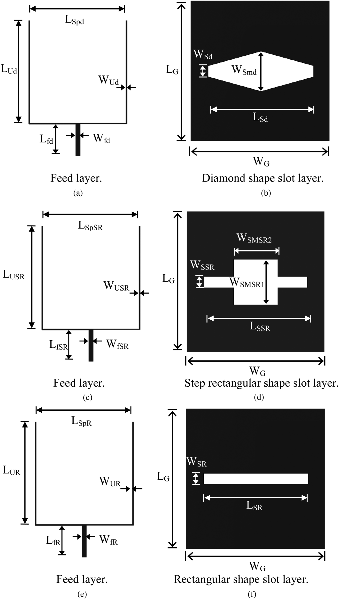
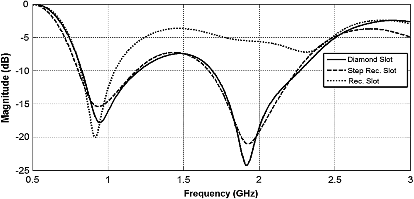
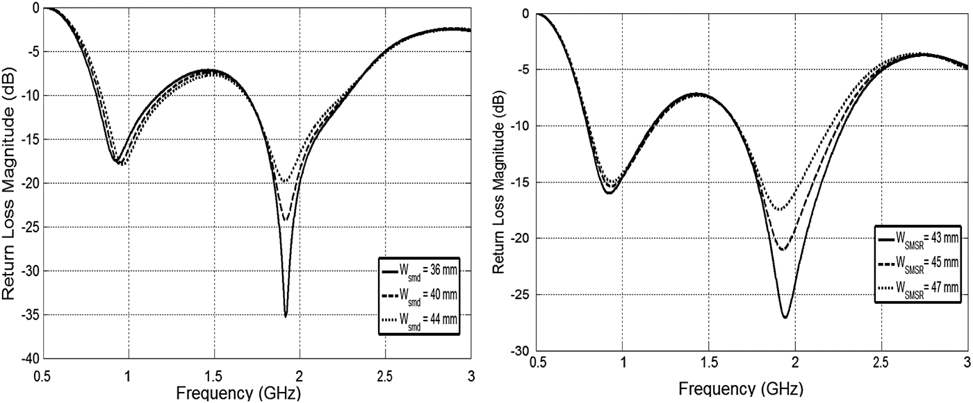
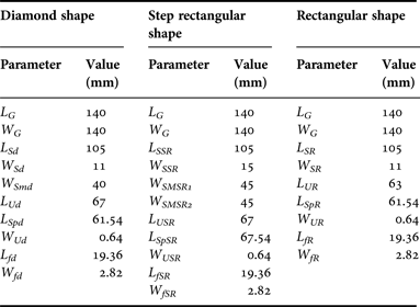
It is difficult to obtain dual-band operation in mobile communication by using the ordinary rectangular slot in the ground plan. An additional parameter is needed to get more control over the generated bands. In this section, two modifications for the rectangular slot are investigated; a diamond shape and a step rectangular shape. The diamond, rectangular, and step rectangular shapes are etched on the ground plane over the FR4 substrate with ε r = 4.5, substrate height (h) = 1.5 mm, and a loss tangent (tan δ) of 0.025. A 50 Ω feed line is branched into two 100 Ω feed lines, which looks like a fork is placed on the other side. Figure 3 shows the configurations of the different slot shapes. Figure 4 illustrates the influence of the slot shape on the operating bands. One can note that all of them have good matching at the lower band that support (GSM900) but there is no matching at the upper bands (DCS1800/PCS1900/UMTS2100) for the rectangular slot shape and there is a good matching at both of the operating bands for the diamond and the step rectangular slot shape. The dimensions of the three configurations are listed in Table 1. Figure 5 shows the parametric study of the different dimensions for the slot middle widths W Smd and W SMSR for the diamond shape and the step rectangular shape.
Fig. 3. The configurations of the three different slots.
Fig. 4. Return loss comparisons between the diamond, the step rectangular, and the rectangular slots.
Fig. 5. Return loss for different dimensions of slot middle widths: (a) slot middle widths W Smd.
Table 1. Geometric dimension of the three different shapes.
III. PROPOSED ANTENNA: GEOMETRY AND DESIGN PARAMETERS
A) Antenna geometry
The geometry of the proposed slot antenna is shown in Fig. 6. The proposed antenna consists of four metallic layers arranged from up to down as follows: port 1 fork feed layer, ground plane with etched cross-slot, port 2 fork feed layer, and two reflectors. The upper reflector is placed at a quarter wavelength apart from the radiating slot at the centre frequency of the upper band and the lower reflector is placed at a quarter wavelength apart from the radiating slot at the centre frequency of the lower band. The FR4 substrates are utilized in the antenna fabrication in order to ensure its rigidity.
Fig. 6. Antenna layers and its side view.
The antenna consists of five layers of dielectric substrates; three layers of FR4 dielectric material and two air gaps. The one air gap exists between the port 2 feed layer and the first reflector (the upper reflector) while the other air gap exists between the substrate that has a relative dielectric constant of 4.5, a dissipation factor of 0.025, and a dielectric thickness of 1.5 mm for the two reflectors.
The port 1/port 2 feed layers consist of an input microstrip line of 50 Ω width branched into two 100 Ω microstrip lines that excite the radiating slot symmetrically. The overall antenna dimension is about 300 × 300 × 73.175 mm3.
The antenna dimensions are: W f = 2.82 mm, L f = 14.36 mm, L U = 71 mm, W U = 0.64 mm, L S1 = L S2 = 107 mm, W S1 = W S2 = 11 mm, L G = W G = 140 mm, W sm1 = 36 mm, W sm2 = 40 mm, L SP1 = 72.54, L SP2 = 71.54 mm, L p = W p = 99 mm, h 1 = h 2 = h 4 = 1.5 mm, ε r1 = ε r2 = ε r4 = 4.5, h 3 = 35 mm, h 5 = 32 mm, and ε r3 = ε r5 = 1.
The radiation layer consists of two diamond cross-slots etched on the metallic ground plane. A diamond slot etched on the ground plane is utilized to achieve the dual-band operation used in mobile communication bands rather than the rectangular slot due to the inclined rib of the diamond shape slot where more desired modes/bands used in mobile operations will be excited. The length of the slot antenna controls the first band (GSM850/GSM900). In order to excite the second mode/band (DCS1800/PCS1900/UMTS2100) many reported works have been conducted such as, placing stacked patches and a reactive loading patch antenna to obtain the second band of the mobile phone communication systems together with the first band. The inclined rib of the diamond shape slot excites the second band (DCS1800/PCS1900/UMTS2100), in conjunction with the first band.
In order to achieve dual-polarized antenna operation, the etched cross-slot with the two orthogonal microstrip feeds looks like a U-shape placed underneath the FR4 substrate material on the opposite side of the ground plane is used. Since the two feeding network layers are separately isolated therefore no air bridge may be used. The symmetry of the feeding branched network is necessary for obtaining high isolation between the two ports and providing good polarization. The configuration of the U-shaped/dual offset feed does not suffer from the increased cross-polarization introduced by a single offset feed line.
The FBR is the most important parameter in this antenna application, which is almost achieved on one band and deteriorates on the other. The FBR is improved by placing two reflectors underneath the radiating slot (AMC). The first square reflector of length 0.3λ 0L (where λ 0L is the wavelength at the lower frequency band 915 MHz) is placed at λ 0U/4 apart from the radiating slot at 1940 MHz (λ 0U is the wavelength at the upper frequency band) acting as a radiator at the lower band (915 MHz) and as a reflector at the upper frequency band (1940 MHz). The second square reflector is placed at λ 0L/4 apart from the radiating slot at 915 MHz.
B) Results and discussions
A prototype of the antenna element with optimized dimensions has been simulated using CST STUDIO SUITE 2011 and then fabricated using the photolithographic process. Figure 7 depicts the simulated return loss for both of the port 1/port 2 sides and the simulated isolation characteristics between the two ports compared to the measured results. As shown in Fig. 7, the antenna covers the GSM850, the GSM900, the DCS1800, the PCS1900, and the UMTS2100 bands at both of the ports.
Fig. 7. Measured and simulated return loss and insertion loss at the transmitting and the receiving bands.
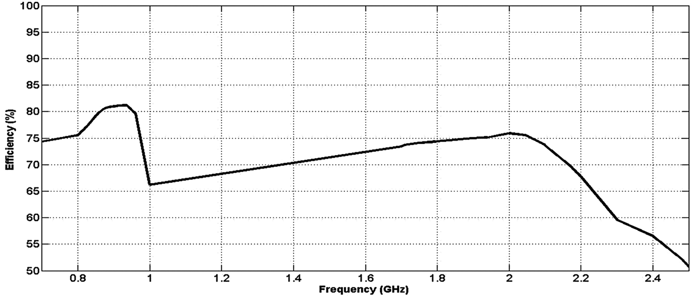
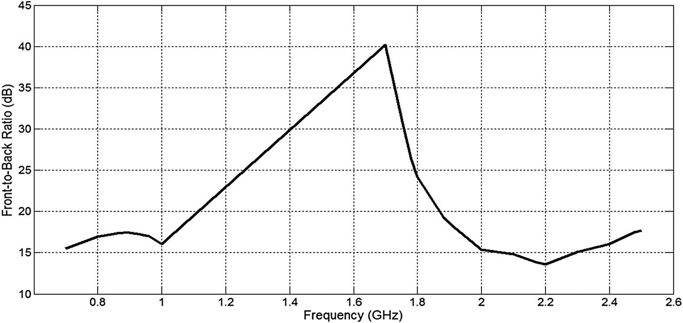
The obtained results reveal that the measured impedance bandwidth (VSWR ≤ 2) at GSM850/GSM900 approaches 255 MHz at port 1 and 281 MHz at port 2, while it approaches 883 MHz at port 1 and 915 MHz at port 2, which covers the DCS1800, PCS1900, and UMTS2100. The measured isolation characteristics/port decoupling between the two ports is noticed to be better than 30 dB at the lower band while it is <40 dB at the upper band. It is clearly observed that dual and wide operating bandwidths are obtained. The proposed antenna is measured using the vector network analyzer Agilent 8719ES. Figure 8 shows the antenna efficiency versus the operating frequency. It is clear from Fig. 8 that the average efficiency at the lower band (GSM900) is about 80% and at the upper bands (DCS1800/PCS1900/UMTS2100) is about 75%. Figure 9 depicts the FBR for the proposed antenna over the operating bands of the frequency, respectively.
Fig. 8. FBR for the proposed antenna.
Fig. 9. The far-field patterns (E-plane and H-plane) at (a) 915 MHz, (b) 1795 MHz, (c) 1920 MHz, and (d) 2045 MHz.
Figure 10 illustrates the measured and the simulated co- and cross-polar E- and H-plane radiation patterns at each of the four operating bands. The radiation pattern was measured in the Science and Technology Centre of Excellence (STCE), Egypt, using compact multi-probe antenna test station (STARLAB-18), VNA model: Agilent E8363B (10 MHz–40 GHz).
Fig. 10. Measured and simulated co- and cross-polar E- and H-plane radiation patterns at (a) 915 MHz, (b) 1795 MHz, (c) 1920 MHz, and (d) 2045 MHz.
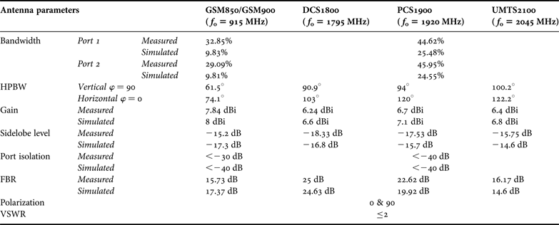
The results are summarized in Table 2. In the future, the antenna element will be used as a basic module for base-station linear arrays, whose final size will depend on the beamwidth and the gain requirements in the elevation plane.
Table 2. Antenna parameters for both the lower bands (GSM850/GSM900) and the upper bands (DCS1800, PCS1900, and UMTS2100)
IV. CONCLUSION
In this paper, a multi-band dual-polarized antenna of diamond shaped cross-slot is introduced. The antenna covers the GSM850, the GSM900, the GSM1800, the PCS1900, and the UMTS2100 bands. The measured bandwidth is sufficient to cover these bands. The antenna is used for transmitting or receiving signals at the same time with measured isolation between the ports <−40 dB at the upper band and −30 dB at the lower band. The antenna introduces a high FBR in all of the operating bands through the introduction of the two reflectors at the two quarter wavelengths, GSM900 and DCS1800. Measured sidelobe level, gain, port isolation, FBR and far-field pattern (E-plane and H-plane) at GSM850/GSM900, DCS1800, PCS1900, and UMTS2100 are presented.
ACKNOWLEDGEMENTS
This work was conducted under a contract between the National Telecom Regulatory Authority (NTRA), the Ministry of Communications and Information Technology (MCIT), Egypt, and the Electronics Research Institute (ERI), Ministry of Scientific Research, Egypt.
Mohamed S. El-gendy received a B.Sc. degree in Electronics and Communication Engineering from the University of Menofia in 2003 and received his M.Sc. degree from Ain Shams University in 2011. His M.Sc. is Self-Diplexed Integrated Microstrip Antenna Front-End Transceiver for Wireless Applications. He is now a Research Assistant at the Electronics Research Institute (ERI), Giza, Egypt. His main research interests are the design and the implementation of mobile base-station antennas.
Haythem H. Abdullah received a B.Sc. degree in Electronics and Communication Engineering from the University of Benha, Egypt in 1998 and received his M.Sc. and Ph.D. degrees from Cairo University in 2003 and 2010, respectively. His M.Sc. is dedicated to the simulation of dispersive materials in the Finite Difference Time Domain Numerical Technique and its application to the SAR calculations within the Human head. The Ph.D. is dedicated to radar target identification. He is now employed as a researcher at the Electronics Research Institute (ERI), Giza, Egypt. His current research interests are the design and the optimization of microstrip antenna arrays and their applications.
Esmat A. Abdallah graduated from the Faculty of Engineering and received her M.Sc. and Ph.D. degrees from Cairo University, Giza, Egypt, in 1968, 1972, and 1975, respectively. She was nominated as Assistant Professor, Associate Professor, and Professor in 1975, 1980, and 1985, respectively. In 1989, she was appointed President of the Electronics Research Institute (ERI), Cairo, Egypt, a position she held for about 10 years. She became the Head of the Microstrip Department, ERI, from 1999 to 2006. Currently, she is at the Microstrip Department, Electronics Research Institute, Cairo, Egypt. She has focused her research on microwave circuit designs, planar antenna systems, and non-reciprocal ferrite devices, and recently on EBG structures, UWB components and antenna, and RFID systems. She acts as a single author and as a coauthor on more than 160 research papers in highly cited international journals and in the proceedings of international conferences in her field.