


INTRODUCTION
Silicon carbide (SiC) is a promising material for its excellent electrical, thermal, and optical properties. SiC single crystals are widely used in various applications of high-power, high-frequency, and high-temperature devices under harsher environmental conditions compared with silicon (Wesch, Reference Wesch1996). Development of reliable and reproducible contacts of metal with SiC is a key technological problem in SiC device processing.
Among metals, platinum (Pt) is the material of choice when a high-oxidation resistance is required for metallic components within devices postprocessed or operated at elevated temperatures. Pt is also a base material for a large variety of different electrodes or within chemical sensors (Grosser et al., Reference Grosser and Schmid2010). Pt can react with SiC to form Pt-silicides: Pt3Si, Pt12Si5, Pt2Si, Pt6Si5, and PtSi (Rijnders et al., Reference Rijnders, Kodentsov, van Beek, van den Akker and Van Loo1997; Xu et al., Reference Xu, Wang, Liu and Jin2008). Papanicolaou et al. (Reference Papanicolaou, Christou and Gipe1989) and Bourenane et al. (Reference Bourenane, Keffous and Nezzal2007) reported that Pt is used for the fabrication of a good Schottky contact with a SiC single-crystal substrate throughout the annealing sequence, and studies of interface electrical property of Pt/SiC joints revealed that the contact resistivity depends on annealing parameters, thickness of a Pt film and phases involved at the interfaces (Bermudez et al., Reference Bermudez and Kaplan1990; Chen et al., Reference Chen, Kolawa, Nicolet, Ruiz, Baud, Jaussaud and Madar1994; Porter and Davis, Reference Porter and Davis1995). An increase of Schottky barrier height (SBH) can be controlled from the grain growth and the film homogeneity at the surfaces.
Studies on Pt, Pt/Ta, Pt/Ti films deposited on glass and SiO2/Si substrates were recently reported by Avrekh et al. (Reference Avrekh, Monteiro and Brown2000), Schmid and Seidel (Reference Schmid and Seidel2008), Grosser and Schmid (Reference Grosser and Schmid2009), and Grosser and Schmid (Reference Grosser and Schmid2010), whereas only few studies on the electrical resistance of Pt films deposited on SiC substrates. The resistivity of Pt films was found to be dominated by grain boundary scattering for films with thicknesses below 5 nm. It should be noted that no chemical reaction between the metal films and their substrates for those contacts was found. Therefore, it will useful to study the electrical resistivity of Pt super-thin films on SiC substrates after annealing at different temperatures.
In this study, we measured room-temperature electrical resistivity of magnetron-sputtered platinum super-thin films (2 nm thick) deposited on 6H-SiC (0001) substrates and studied interfacial reactions between the 2-nm Pt films and their SiC substrates. Local characteristics of surface and interface morphology evolution of Pt/6H-SiC (0001) contacts after annealing between 400 and 1000 °C were also investigated. The origins of microstructures on the film surfaces and interfacial reactions will also be discussed.
EXPERIMENTAL
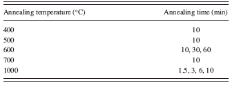
Commercial grade n-type 6H-SiC single crystal wafers (TankeBlue Semiconductor Co., Ltd.) were used with carrier concentrations of 1016–1017 cm−3. An epi-ready wafer of 337 μm thick was cut into 10 × 10 mm2 pieces, and then each piece was sputtered with a 2-nm platinum film with purity of 99.99 wt. % by an AJA ATC-1800F nanomagnetic film sputter. Each sample was annealed in a muffle furnace after being sealed in a separated quartz tube with vacuum degree of 5 × 10⁻⁵ Pa. Details on the temperature and time used for the annealing process are given in Table I.
An atomic Force Microscopy (AFM, Dimension V), a field-emission scanning electron microscopy (SEM, SUPRA 55) and an Auger electron spectroscopy (AES, ULVAC PHI-700) were used to characterize reaction zones and morphology of contacts. A Philips X’PERT Pro X-ray polycrystal diffractometer with Cu Kα radiation, an X-ray Photoelectron Spectroscopy (XPS, ULVAC-PHI Quantera SXM) and a Raman microspectroscopy (Nicolet) were used to identify phase formation and structures of the Pt/SiC contact. Current–voltage (I–V) characterizations were carried out by a four-probe method with Keithley 220 Current Sources Power Supplies and Keithley 2000 Voltage Sources Power Supplies. Figure 1 depicts the geometry schematic diagram of the four-probe setup for the I-V measurements.
TABLE I. Annealing temperature and time.
RESULTS AND DISCUSSION
Morphology
Figures 2a – 2f show the evolution of AFM images of the samples in the contact mode. The substrate and the as-deposited sample, shown in Figures 2a and 2b, exhibit a uniform surface with the same Root-Mean-Square (RMS) of roughness of 0.2 nm. Figure 2c represents the islands scattering on the surface of the sample annealed at 600 °C for 10 min. This result agrees with the work of Bermudez et al. (Reference Bermudez and Kaplan1990), where Pt films (≤0.8 nm thick) were deposited on cubic β-SiC (001) surfaces, and also compatible with the case of a Pd film on a SiC substrate (Veuillen et al., Reference Veuillen, Tan, Tsiaoussis, Frangis, Brunel and Gunnella1999; Tsiaoussis et al., Reference Tsiaoussis, Frangis, Manolikas and Tan2007). The reason for the island growth on a SiC single crystal substrate may come from crystal lattice mismatch at the interface and inhomogeneous stress induced by the thermal process of the Pt/SiC interface.
From the AFM image of Figure 2c, the mean height of the islands is about 1–2 nm with a mean width of 120 ± 10 nm, and the distance between two neighboring islands is about 250 nm. When annealed at 700 °C for 10 min as shown in Figure 2d, the islands on the surface appear to be denser, indicating the progress of an interface reaction to form separate islands with a mean height of 4 ± 1 nm and width of 275 ± 25 nm. The distance between two neighboring islands is about 200 nm [see Figure 4a]. For the sample annealed at 1000 °C for 10 min as shown in Figure 2e, similar aggregation of islands is also observed with 6 ± 2 nm in height and 320 ± 25 nm in width. Meanwhile, the surface is more homogeneous. Therefore, the island sizes become larger with increasing annealing temperature [see Figure 2f]. Porter et al. (Reference Porter and Davis1995) reported that the increase in the sizes of the islands indicates that preferential grain growth with annealing occurred in order to decrease the strain associated with the interface. Moreover, a comparison of our AFM images on the samples annealed at 600 °C for 10, 30, and 60 min shows that the sizes of the islands

Figure 1. (Color online) Geometry schematic diagram of four-probe setup for I-V measurement.

Figure 2. (Color online) AFM images of the samples: (a) substrate (b) as-deposited, (c) annealed at 600 °C for 10 min, (d) 700 °C for 10 min, and (e,f) 1000 °C for 10 min, The size of the selected area is 10 × 10 μm2 for Samples a, b, c, d, e and 3 × 3 μm2 for Sample f.
become larger while the number of islands became smaller with increasing annealing time.
Structure, composition and reaction mechanism
To identify the crystalline phases presented in the islands, XRD measurements were performed. The XRD pattern of sample annealed at 1000 °C for 10 min is shown in Figure 3a. The results indicate that PtSi and Pt2Si are formed at 1000 °C. By comparing the Gibbs energies of formation between Pt silicides (Xu et al., Reference Xu, Wang, Liu and Jin2008) and SiC (−54 kJ·mol−1 at 1000 °C), an reaction between Pt and SiC (e.g., xPt + ySiC = PtxSiy + yC) is thermodynamically favored. Therefore, it proves that Pt reacted with SiC to form a series of silicides with different stoichiometric compositions. The Pt-4f core level X-ray photoelectron spectra for the 500- and 600- °C samples were shown in Figure 3b. The annealing process caused a negative shift in the binding energy of the 4f7/2 signal of the zero-valent platinum species (at ∼71 eV), which means Pt atoms reacted with Si from the substrate even at annealing temperature of 500 °C.
Figure 4a is the SEM image of the sample annealed at 700 °C for 10 min. It shows that the thin film consists of lighter contrast parts, corresponding to the islands detected

Figure 3. (Color online) (a) XRD pattern of the sample annealed at 1000 °C for 10 min, (b) XPS spectra of Pt-4f core-levels for as-deposited, 500 and 600 °C-annealed samples.
by AFM observation in Figure 2c, and flat regions (in dark areas). The energy dispersive spectrum (EDS) data on A and B points in Figure 4a reveal the presence of Pt (2.49 at. %), Si (31.32 at. %), and C (66.18 at. %) in the island area, whereas no Pt was detected in the flat region. Moreover, the amount of carbon is higher than that of silicon in both regions.
To study the distributions of Pt, Si, and C across the Pt/SiC contact zone, AES depth profiles of the sample annealed at 600 °C for 10 min were obtained and analyzed [see Figure 4b]. It was found that the top surface of <1-nm depth composes of 95% and C and the remaining 5% of Si, Pt, and O. Similar elemental distributions were also observed by other investigators when contact metals were Pd (Veuillen et al., Reference Veuillen, Tan, Tsiaoussis, Frangis, Brunel and Gunnella1999) and Ni (Juang et al., Reference Juang, Wu, Lo, Chen, Huang, Hwang, Chen, Leou and Tsai2009; Zhang et al. Reference Zhang, Teng, Yuan, Zhang and Chen2009). The reaction zone is estimated to be 4 nm, since the carbon concentration first fell down and then remained the same beyond this sputtering depth. Pt concentration was found to go up to a maximum of 18% of Pt at 2-nm depth and then decreases slowly. These results indicate that Pt diffused into the interface and carbon moved toward the surface. It is worthy to be noted that a nonstoichiometric Si:C ratio (less than 1:1) in bulk SiC was shown in the AES profile. The reason might be resulted from an inclusion of carbon during the growth of the SiC single-crystal substrate.
The results of our structure and chemical analyses show that the interface reaction mechanism can be described as: (1) Pt, aggregating into islands, first diffused into the SiC substrate; (2) Further annealing induced chemical reactions between Pt and SiC to produce Pt silicides (PtxSiy) and free carbon; (3) Pt silicides, whose ratio of Pt and Si depends on the annealing temperature, stayed in island morphology on the surface; (4) Due to low solubility and composition gradient, free carbon precipitated to a larger concentration after annealing and diffuses outward the relatively loose reaction zone to spread throughout the surface. Figure 4c gives a schematic diagram of phase evolution of Pt (2 nm)/6H-SiC (0001) contacts as annealing temperature increasing.
Carbon structure
The influence of annealing process on the structure of carbon layer is further investigated. Raman spectra of the samples annealed at various temperatures performed using the excitation laser wave length of 532 nm is shown in Figure 5a. The peaks in Raman shift of 1520 and 1715 cm−1 are the characteristics of 6H-SiC (Burton et al., Reference Burton, Sun, Long, Feng and Ferguson1999). The graphite materials exhibit three characteristic peaks: D-band at Raman shift ∼1350 cm−1, G-band at ∼1580 cm−1, and 2D-band at ∼2700 cm−1 (Ferrari et al., Reference Ferrari, Meyer, Scardaci, Casiraghi, Lazzeri, Mauri, Piscanec, Jiang, Novoselov, Roth and Geim2006; Pimenta et al., Reference Pimenta, Dresselhaus, Dresselhaus and Canc2007). All of the peaks in Figure 5a can be pointed to characteristics of 6H-SiC and carbon. The D bands of carbon become narrower and more symmetric with increasing annealing temperature. The G bands for all the samples move to a higher frequency than highly oriented pyrolytic graphite (HOPG, 1580 cm−1) (Baba et al., Reference Baba, Nagata, Takahashi, Nakamura, Yoshiyasu, Sakurai, Yamada, Ohtani and Tona2005), which might arise from the internal stress existed in the layer interface during the thermal process. It is worthy to note that the 2D peak at 2708 cm−1 is distinguished in Figure 5a only for the sample annealing at 1000 °C. This peak, exhibiting a relatively broad and asymmetrical feature, indicates the formation of few-layer microcrystalline graphite with several nanometers (Ferrari et al., Reference Ferrari, Meyer, Scardaci, Casiraghi, Lazzeri, Mauri, Piscanec, Jiang, Novoselov, Roth and Geim2006). It is also found that the D peak of this sample presents stronger intensity than the G band, which means an indication of higher disorder degree, caused by a defect-assisted one-phonon double resonance effect (Pimenta et al., Reference Pimenta, Dresselhaus, Dresselhaus and Canc2007). Therefore, the layer number and crystallinity of carbon on the surface is dependent on the annealing parameters. At a low annealing temperature, the interface reaction produces amorphous carbon. Crystalline carbon forms at high temperatures (e.g. 1000 °C). In fact, a thin-layer carbon film can be prepared by tuning the reaction between the metal film and its SiC substrate by film thickness, annealing temperature and time (Juang et al., Reference Juang, Wu, Lo, Chen, Huang, Hwang, Chen, Leou and Tsai2009). This is also verified by our other work on a Co film on SiC substrate (Li et al., Reference Juang, Wu, Lo, Chen, Huang, Hwang, Chen, Leou and Tsai2011).
Raman spectra of the samples annealed at 1000 °C for various times are shown in Figure 5b. The intensity ratios of D- and G-peak (ID/IG), valued at around 1.0, increase slightly with increasing annealing time. The 2D peaks are

Figure 4. (Color online) (a) SEM images of the sample annealed at 700 °C for 10 min and chemical composition by EDS analysis of A and B parts. (b) AES depth profiles of the sample annealed at 600 °C for 10 min. and (c) Schematic diagram of phase evolution of Pt/SiC contacts during the annealing process.
not clearly observed for the samples annealed for shorter times. The reaction mechanism discussed above suggests that a shorter annealing process may generate fewer products presenting a thinner reaction zone, and thus, carbon diffuses easily outward the surface. However, when annealing for a longer period, the reaction did produce a thicker reaction zone. Therefore, graphite atom diffusing to the surface throughout the reaction zone would be limited, which resulted in a strong 2D band at 2708 cm−1 in Figure 5b.
Electrical property
Figure 6 shows the room-temperature current–voltage characteristics of the Pt films deposited on SiC single crystal substrates as a function of annealing temperature. The as-deposited sample exhibits a lower electrical conductivity compared to that of bulk Pt. This is due to the quantum size effect of the Pt film. With annealing temperature increasing to 600 °C, the slope rose up to 1.47 × 10⁻² from 8.59 × 10⁻⁴ S, suggesting a reduction in film electrical resistance. When the annealing temperature increased to 1000 °C, the I–V characteristics (see the insert of Figure 6) changed dramatically with a large slope of 1.43 S, around a 100-fold enhancement than that of the sample annealed at 600 °C for 10 min.
The reason for annealing temperature dependence on electrical property of the thin films was investigated. From the surface-morphology analysis, it is shown that the sample surface evolved from isolated islands to continuous film with the annealing temperatures increasing. It is well known that the motion mechanism of electron between unconnected islands mainly bases on thermionic emission theory. Thus, the electrical conductivity became better as the distances between separated islands became smaller. In other words, the film resistivity decreased because of grain growth and homogeneity of the films increased with increasing temperature. Additionally, the formation of Pt silicides and a thin layer of crystalline graphite on the sample surface, which produced by the selective interface reactions between Pt and SiC, might be accounted for the dramatic enhancement of the observed electrical characteristics. Geim and Novoselov (Reference Geim and Novoselov2007) reported that a thin-layer graphite, also named as graphene, exhibited unconventional electronic properties, such as high mobility at room temperature for both electron and hole conductions.
The effect of substrate temperature on the film resistivity was also studied. The electrical measurements showed an enhancement of the ratio of I and V when the substrate is heated to 450 °C (see Figure 6). AFM measurements in this work showed that the increase of substrate temperature for the as-deposited sample did not change largely the surface morphology compared with that on the substrate at room temperature. The Raman spectra also showed that there is no characteristic carbon peak, which means the interface reaction between Pt and the heated substrate did not occur before annealing. However, when Pt was deposited on a hot SiC substrate, it increased the diffusion rate of Pt into SiC substrate and thus resulted in a decrease in the film resistance.
CONCLUSION
We have deposited Pt films (2-nm thick) on clean 6H-SiC substrates, subsequently annealed from 400 to 1000 °C

Figure 5. (Color online) The Raman spectra of samples: (a) annealed at 400, 500, 600, and 1000 °C for 10 min. (b) annealed at 1000 °C for 1.5, 3, 6, and 10 min. The spectra of 6H-SiC are used for a reference.

Figure 6. (Color online) Current-Voltage characteristics of samples annealed at 400, 600, 1000 °C for 10 min compared to those of unannealed samples deposited at room temperature (RM) and 450 °C.
for various times. The selective interface reactions between Pt and Si dissociated from the SiC substrate during annealing led to the formation of Pt silicide islands. The height and width of the islands became higher and bigger with increasing annealing temperature. Meanwhile, the islands aggregated to enhance the film homogeneity at higher annealing temperatures. The increase in electrical conductivity for the samples annealed at 400 to 600 °C might be accounted for the decreased transmission blocks on the surfaces. The formation of Pt silicides and a thin layer of crystalline graphite for the sample annealed at 1000 °C, detected by 2D peak in the Raman spectra, was also an origin of the observed high conductivity. Therefore, the optimization of the annealing parameters and substrate temperatures can be used to tune the electrical property of a Pt film on SiC substrate, which would extend the potential applications of SiC-based electronic devices.
ACKNOWLEDGMENTS
The authors thank Dr. L. Q. Guo for the help in AFM measurements and Dr. J. Teng for the help in magnetic sputtering. The financial support by the National Natural Science Foundation of China (Grant Nos. 50772012, 50972010), and the Fundamental Research Funds for the Central Universities (FRF-TP-09-021B) is gratefully acknowledged.


