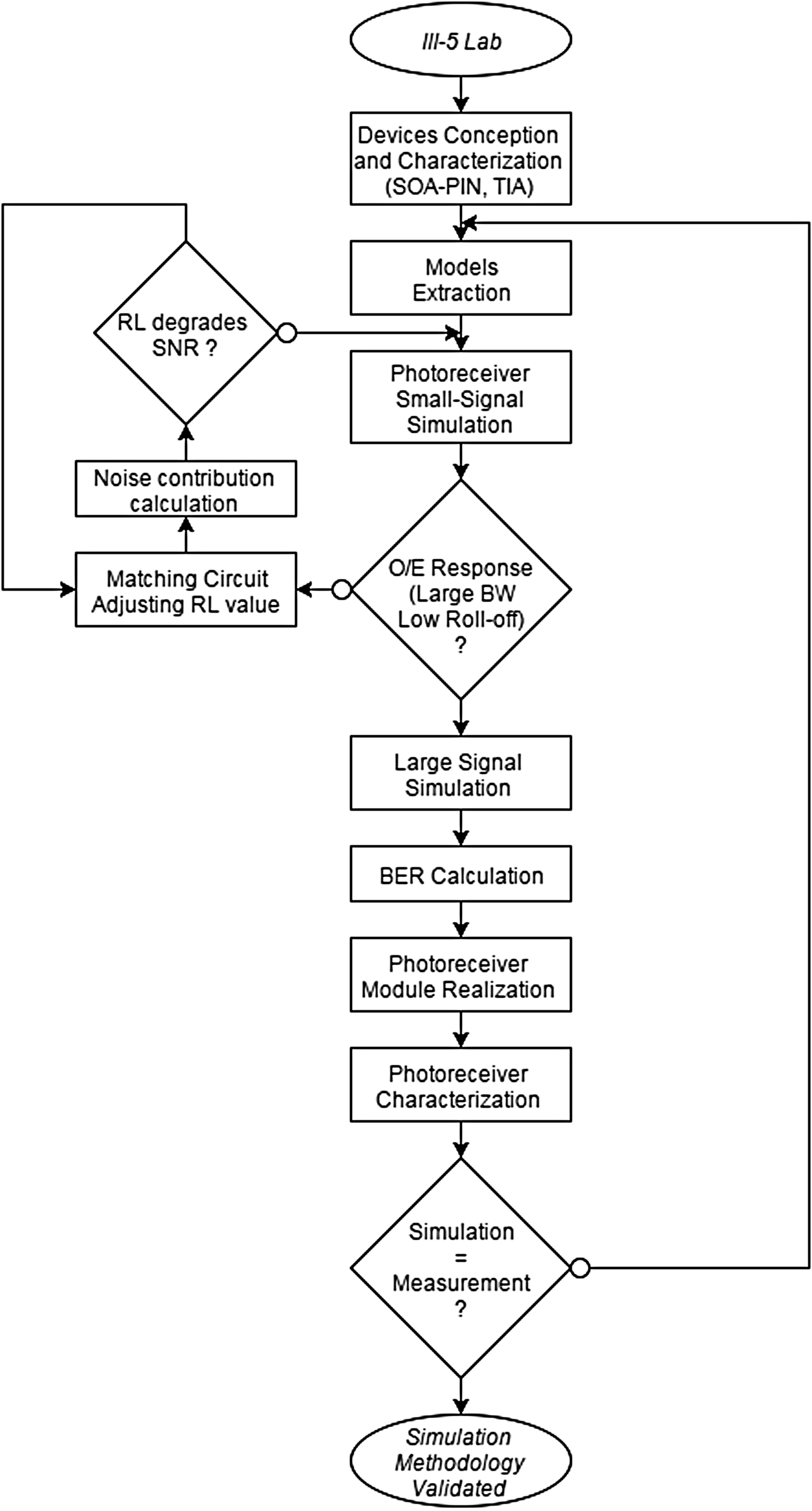
I. INTRODUCTION
Access network transmissions are becoming more and more popular because of the growing need of data. Indeed, the variety of multimedia services and the increasing amount of internet users force the already set short reach communication network to evolve continuously. 2.5 Gb/s capable Gigabit Passive Optical Network (GPON) and Ethernet Passive Optical Network (EPON) are the currently deployed Passive Optical Network (PON) architecture. Next generation 10G-PON (10 Gb/s) have been standardized and are about to be deployed. From the perspective of a longer-term vision, higher bandwidth system and technologies are already studied, in order to be able to reach 40 Gb/s capable PON architecture [1]. The presented module has been developed to demonstrate the capability of a single wavelength working photoreceiver to reach very high gain and sensitivity at high bit-rate and simple modulation format, such as 40 Gb/s NRZ. This would provide a lower-cost solution for 40 Gb/s transmissions, compared to multi-wavelength or advanced modulation format which need complex and more expensive transceivers. A post-amplified receiver [Reference Vetury2] and a pre-amplified receiver [Reference Mason3], exhibited a sensitivity for a bit error rate (BER) of 10−9 of −10.5 and −17.5 dBm, respectively. This paper addresses the problems associated with the integration of the semi-conductor optical amplifier (SOA)-PIN receiver [Reference Caillaud4] with the TIA, and a detailed solution is outlined with simulations and measurements results. The packaging optimization, consisting in using a matching circuit between the photodetector and the TIA leads to a −22.5 dBm sensitivity at a BER of 10−9.
II. PHOTORECEIVER OPERATING PRINCIPLE
A) Direct PIN–TIA integration: bandwidth limitation
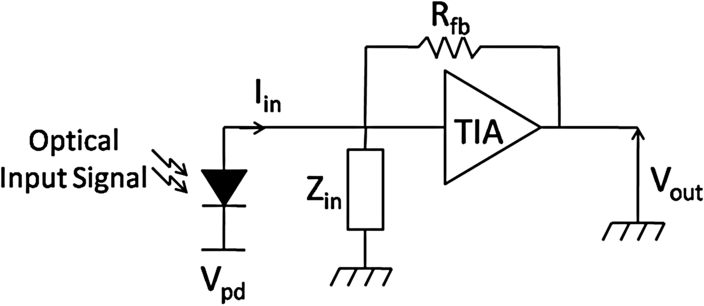
The simplified equivalent circuit of the PIN–TIA integration is shown in Fig. 1.

Fig. 1. Simplified equivalent circuit of the PIN–TIA integration.
Z in symbolizes the combination of the equivalent capacitor of the photodiode C D and the input parasitic capacitor C IN of the TIA. From this circuit, the transfer function V out/I in [Reference Razavi, Paulson and Flomenhoft5] is:
 $$\displaystyle{{{V_{out}}} \over {{I_{in}}}}(\omega ) = - \displaystyle{A \over {A + 1}}.\displaystyle{{{R_{fb}}} \over {1 + ({R_{fb}})/{Z_{in}}(\omega )(A + 1)}},$$
where A is the amplifier voltage gain and R fb is the feedback resistance. The main bandwidth limitation when integrating the photodiode and the TIA is the RC cut-off frequency of the circuit. From equation (1), this cut-off frequency is written as:
 $${f_{{c_{ - 3dB}}}} = \displaystyle{1 \over {2\pi}} \displaystyle{{A + 1} \over {{R_{fb}}{C_T}}},$$
where C T = C D + C IN. For a voltage gain A = 18.5 dB, an equivalent photodiode capacitance C D = 50 fF, an input parasitic capacitance of the amplifier C IN = 160 fF and a feedback resistor R fb = 300 Ω, the calculated cut-off frequency is about 24 GHz.
B) Effect of the matching load on the receiver bandwidth
In order to increase the R fbCT limited bandwidth of the photodiode/TIA integration, a parallel matching resistance R L is integrated between C D and C IN, so that  ${Z_{in}} \equiv {C_D}{\rm \parallel} {R_L}{\rm \parallel} {C_{IN}}$. In that case, the cut-off frequency is given by:
 $${f_{{c_{ - 3dB}}}} = \displaystyle{1 \over {2\pi}} \left( {\displaystyle{{A + 1} \over {{R_{fb}}{C_T}}} + \displaystyle{1 \over {{R_L}{C_T}}}} \right).$$
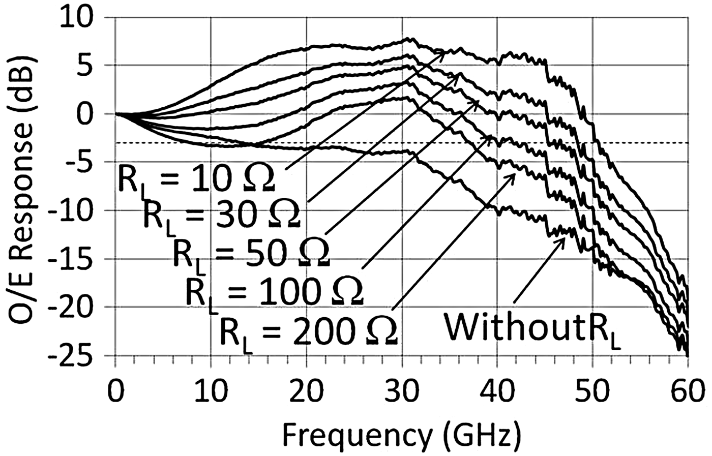
Figure 2 shows the effect of R L on the opto-electrical frequency response of the receiver. When R L > 50 Ω a low-frequency roll-off is observed. This will increase the inter-symbol interferences (ISI) and will limit the high bit rate operation. By decreasing the value of R L, the −3 dB bandwidth is enhanced but the high-frequency peaking effect is also heightened.

Fig. 2. Simulated OE response of the photoreceiver.
III. SIGNAL-TO-NOISE RATIO (SNR)
The SNR is a figure of merit of how well the photoreceiver will detect the transmitted optical signal [Reference Agrawal and Chang6]. Every component constituting the photoreceiver module will contribute to the receiver added noise. The addition of a matching load in the module will deteriorate the SNR, but will be negligible in comparison with the other optical and electrical components. For a pre-amplified SOA-PIN–TIA receiver with integrated matching load, the SNR is written as :
 $$SNR = \displaystyle{{I_s^2} \over {\sigma _{Tot}^2}} = \displaystyle{{{{(G.R.{P_{in}})}^2}} \over {\sigma _{sp - sp}^2 + \sigma _{sig - sp}^2 + \sigma _s^2 + \sigma _{Th}^2 + \sigma _{n,TIA}^{RMS}}}, $$
where R is the photodiode responsivity, G the SOA gain, and P in the optical input power. Before independently developing each noise term appearing in the denominator in Section III.B), the equivalent noise bandwidth (ENB) principle will be explained.
A) Equivalent noise bandwidth
The noise generated in a receiver characterized by a transfer function |H(f)| is the result of the sum of the noise at each frequency. It can be evaluated by integrating the transfer function on the whole frequency range and represented by an ideal filter (brick-wall) with an equivalent area.
Figure 3 shows the normalized transfer function of a first-order RC filter. The blue area represents the transfer function area of the filter with a −3 dB bandwidth equal to 43 GHz. By integrating this area all over the frequency range, the equivalent cut-off frequency of the ideal filter can be determined. Its amplitude is equal to 1 and its width is equal to the ENB. This ideal filter transfer function is represented in red.
Fig. 3. ENB of a first-order filter.
Figure 4 shows the calculated ENB of the photoreceiver module integrating a parallel matching load. It is estimated around 72 GHz. This value will be useful in order to theoretically estimate the noise generated by the photoreceiver.
Fig. 4. ENB of the photoreceiver.
B) Noise contribution of each component
1) SOA-PIN
When biased with a DC current, the SOA emits a broad-spectrum signal called the “amplified spontaneous emission” (ASE). Because of the incoherent nature of the light emitted by the ASE, the output signal will become noisier than the input signal. Two noise contributions are due to the ASE and added to the shot noise of the detector as described in the following equations:
 $$\eqalign{&{\rm Spontaneous} -{\rm spontaneous\;beat\;noise}: \cr & \qquad\;\sigma _{sp - sp}^2 = 4.{R^2}.S_{sp}^2. {\Delta_{{\nu _{sp}}}}.{\Delta_f}.}$$
 $${\rm Signal} - {\rm spontaneous \;beat \;noise}:\;\sigma_{sig - sp}^2 = 4.{R^2}.G.{P_{in}}.{S_{sp}}.{\Delta _f}.$$
 $${\rm Shot} - {\rm noise}:\;\sigma _s^2 = 2.q[R(G.{P_{in}} + {P_{sp}})]{\Delta _f},$$
where  ${P_{sp}} = {S_{sp}}.{\Delta _{{\nu _{sp}}}}$ is the ASE power,
  ${\Delta _{{\nu _{sp}}}}$ is the spectral bandwidth of the ASE, S sp = (G − 1)η sp.h.ν is the ASE spectral density, and Δ f is the electrical noise bandwidth.
2) TIA
The transimpedance amplifier (TIA) noise is generally given as the root-mean-square input referred the noise current value. In the presented photoreceiver, the noise  $\sigma _{n,TIA}^{RMS} $ is calculated from the measured output noise voltage
  $v_{n,out}^{RMS} $ and the transimpedance gain mid-band value R T as :
  $\sigma _{n,TIA}^{RMS} = v_{n,out}^{RMS} /{R_T}$. The minimum TIA input referred noise measured is 5 µA.
3) MATCHING LOAD
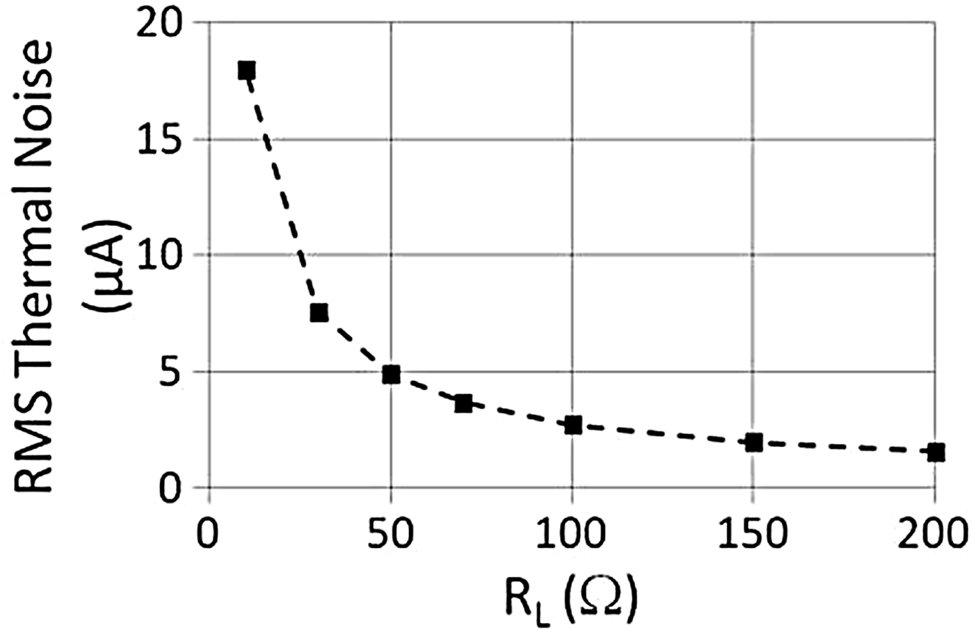
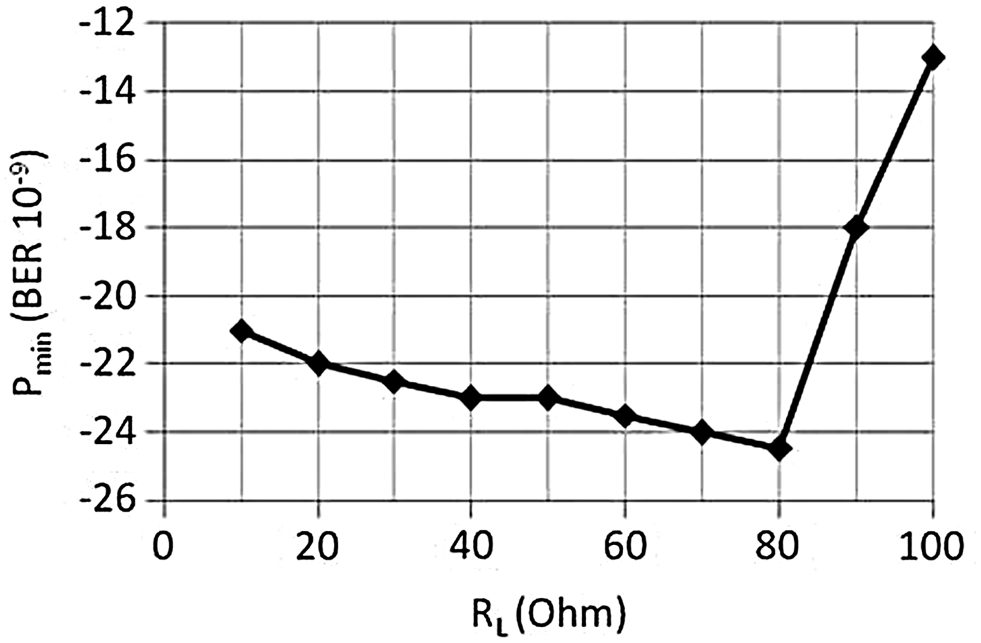
Electrons move randomly in any conductor and for a given temperature T, this movement will manifest as a fluctuating current. The noise variance is given by:  $\sigma _{Th}^2 = 4.k.T/(R){\Delta _f}$. Figure 5 shows the matching load thermal noise, integrated on the equivalent noise bandwidth. The noise remains low (<5 µA) as long as R L ≥ 50 Ω, but it increases up to 18 µA when R L = 10 Ω. Figure 6 shows the impact of R L on the photoreceiver calculated sensitivity, which takes into account the noise, the −3 dB bandwidth and the equivalent noise bandwidth. The maximum sensitivity is obtained for R L = 80 Ω. However, this calculation does not take into account the low-frequency roll-off observed in Fig. 2 for R L value higher than 50 Ω. At R L = 80 Ω the roll-off is still greater than 1 dB, and will certainly degrade the large signal performances. It is only for R L ≤ 50 Ω that the roll-off is totally removed. In conclusion, in order to find the best trade-off between noise, bandwidth and good signal integrity, the chosen value for R L is 50 Ω.
Fig. 5. Theoretical thermal noise.
Fig. 6. R L impact on the theoretical sensitivity.
Figure 7(a) shows the different noise sources calculated from the previous equations, versus the input optical power. As observed previously, the pre-amplified photodetector noise increases with the input optical power. Thus, it will not be identical on the “1” level and the “0” level of the NRZ signal. The SOA gain is about 20 dB for an input optical power of −25 dBm, its noise figure is 8 dB and its optical −3 dB bandwidth is 77 nm. The photodiode responsivity is 0.5 A/W. The signal wavelength is 1550 nm and the ENB is 72 GHz. Figure 7 also shows two measured eye diagram at −12 and −25 dBm, in order to illustrate the noise difference on the one level and the zero level.
Fig. 7. (a) Noise sources of the photoreceiver. (b) 40 Gb/s eye diagram, P opt = −25 dBm (c) 40 Gb/s eye diagram, P opt = −12 dBm.
It is clear that the noise is mainly due to the ASE of the optical amplifier. The matching load, which allows a significant improvement of the −3 dB bandwidth, has a low impact on the SNR when the signal is pre-amplified by a SOA. The BER is calculated from the SNR [Reference Fay7, Reference Caillaud8] and compared with the measurement in Fig. 18(c).
IV. MEASUREMENTS AND SIMULATION RESULTS
A) Devices performances
1) SOA-PIN
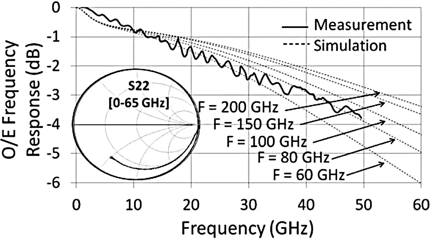
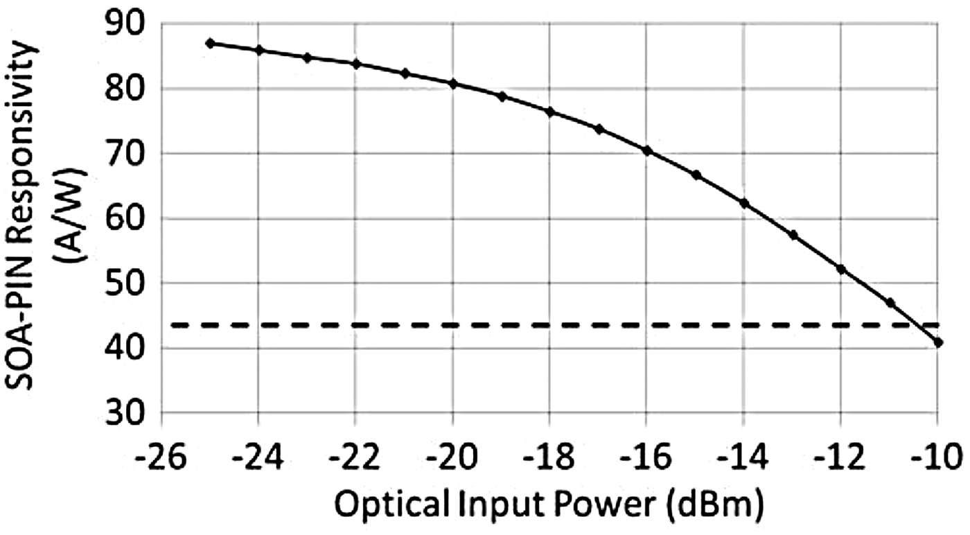
The electro-optic equivalent model of the photodiode is extracted from S-parameter measurements following two steps. The first is to extract values of the electrical circuit lumped elements from reflection measurement. It consists of the junction capacitance C j and the series resistance R s for the active region of the photodiode and a L padCpad model for the transmission line. The measured and simulated reflection coefficient (S 22) of the photodiode is represented in Fig. 8. Good agreement between simulation and measurement validate the electrical model. The second step is to determine the cut-off frequency of the current source I S, which is directly related to the carrier transit time [Reference Lewen9]. To set it in our simulation we measured the O/E frequency response of the photodiode and then adjusted the cut-off frequency of the current source. Figure 8 shows that the transit time cut-off frequency F which fits best with the measurement is about 80 GHz. Figure 9 shows the measured responsivity of the monolithically integrated SOA-PIN depending on the input optical power. The maximum measured responsivity is about 87 A/W and the saturation power of the optical amplifier is about −11 dBm.
Fig. 8. S-parameters of the photodiode.
Fig. 9. Measured SOA-PIN responsivity.
2) TIA
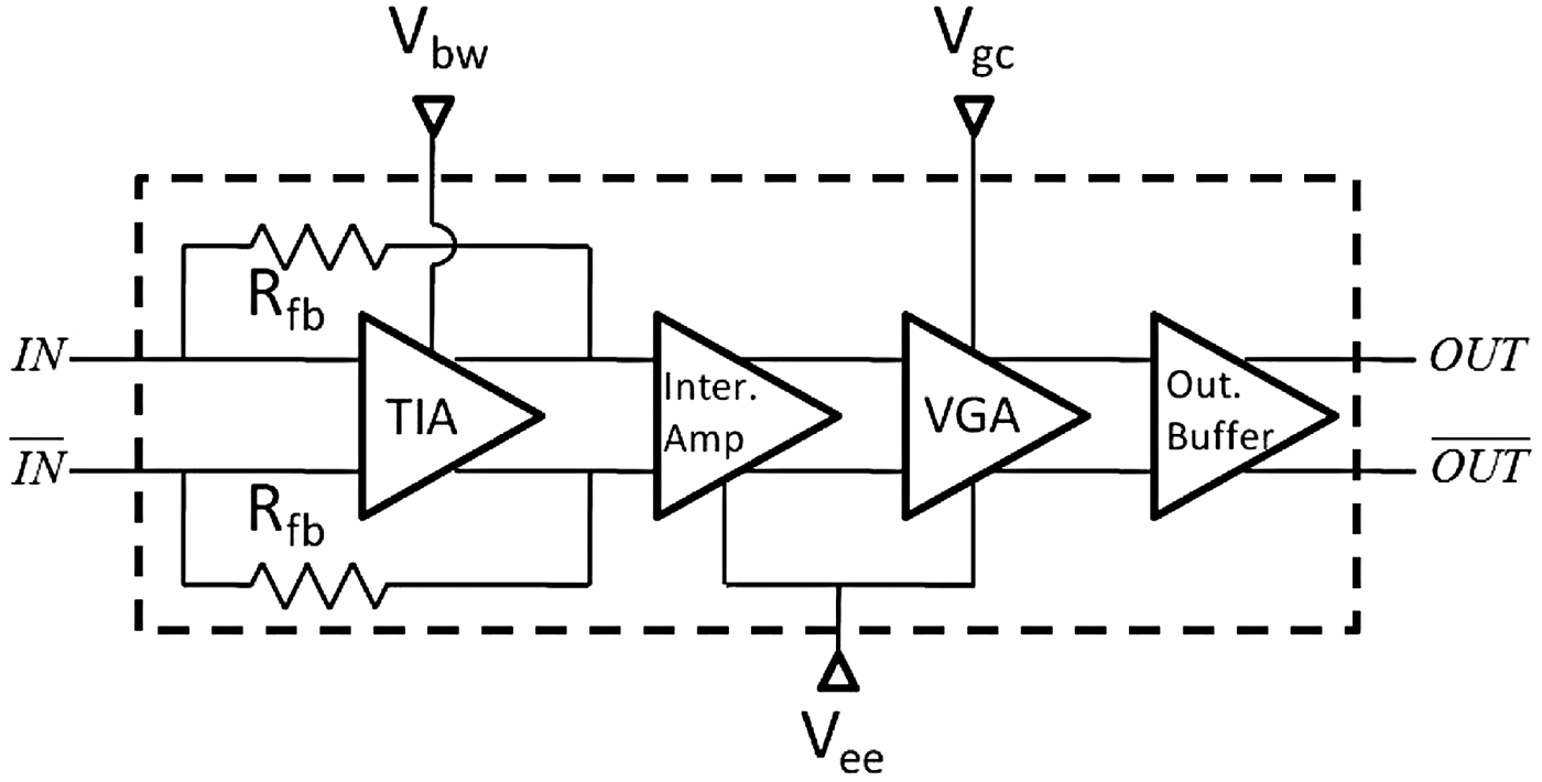
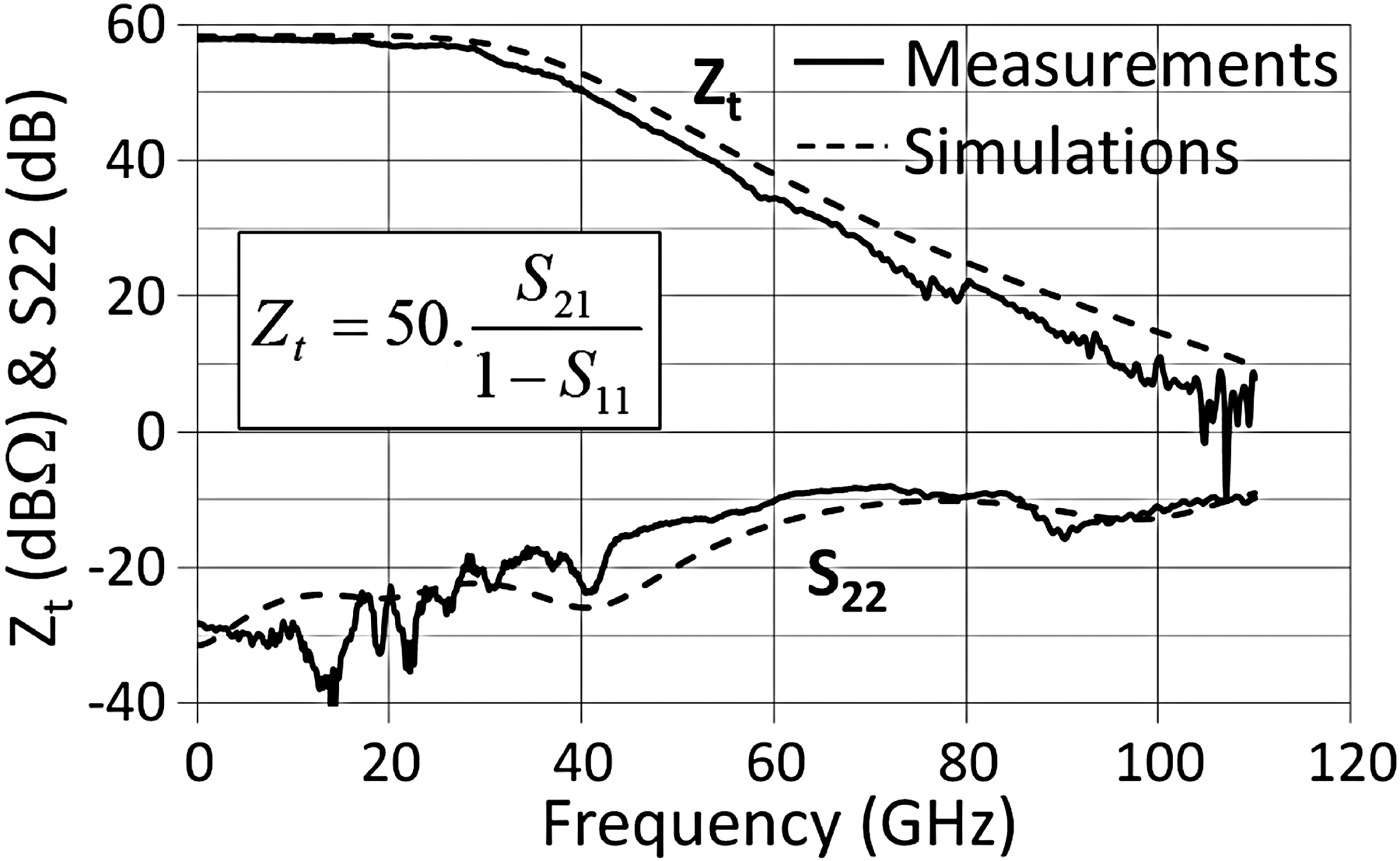
The in-house InP/InGaAs-based variable gain and linear differential TIA used is made of about 40 transistors with  ${f_T} = {f_{max}} = 340\,{\rm GHz}$ (the latest version of the TIA is reported in [Reference Dupuy10]). It consists of three stages as represented in Fig. 10: the transimpedance stage which is designed to have a 300 Ω transimpedance gain, the intermediate amplifier and variable gain amplifier stage based on the Cherry–Hooper [Reference Cherry and Hooper11] architecture and the 50 Ω output buffer. Both bandwidth and gain are adjustable thanks to bias voltages, V bw and V gc, respectively. The full TIA exhibits a single-ended transimpedance gain of 58 dBΩ (≈800 Ω) and an output reflection coefficient below 10 dB up to 60 GHz, as seen in Fig. 11. The TIA model used in simulations takes into account as accurately as possible the effect of the parasitic elements, such as strip lines between each lumped elements. A good agreement is observed between simulation and measurement.

Fig. 10. Variable gain control TIA structure.

Fig. 11. TIA transimpedance gain.
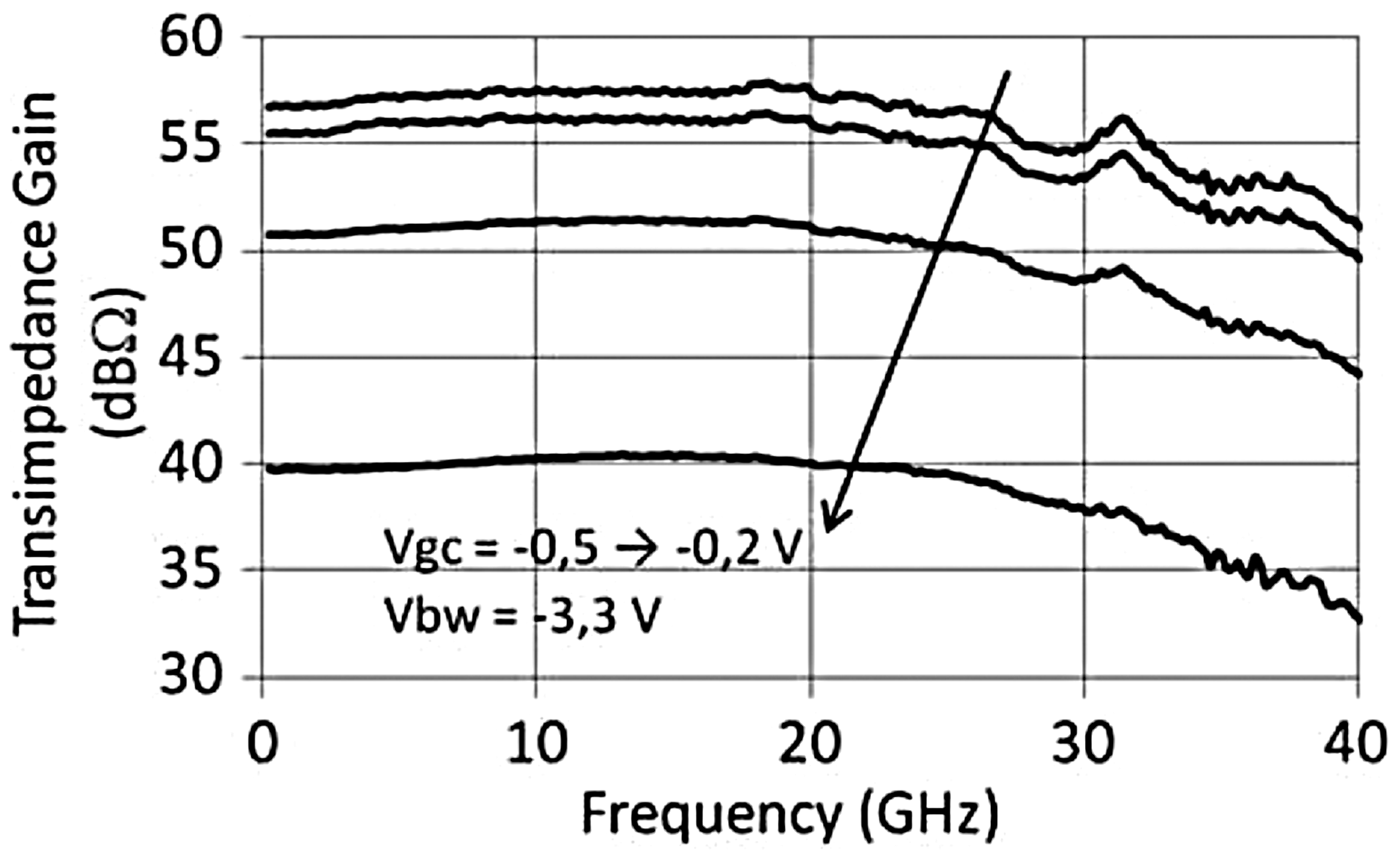
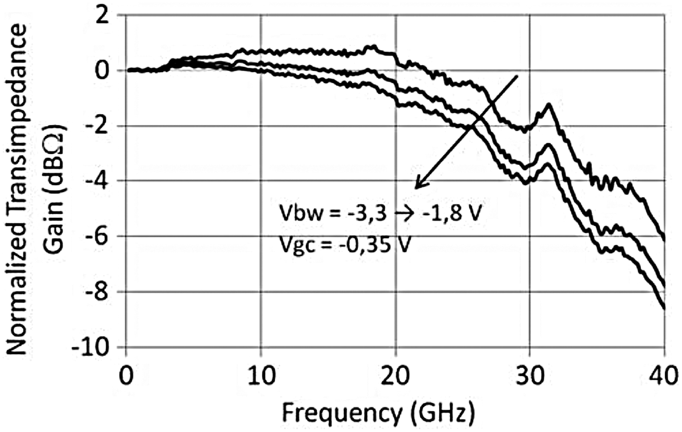
Figure 12 shows the variation of the TIA transimpedance gain depending on the V gc voltage value. In a range of 0.3 V, the transimpedance gain is highly adjustable without modifying the 3 dB bandwidth. Figure 13 shows the normalized transimpedance gain of the TIA. Lowering the V bw voltage of 1.5 V results in a 6 GHz bandwidth decreasing. The effect of these bias voltages on the photoreceiver performances will be observed and quantified in Sections IV.C and IV.D.

Fig. 12. Gain control (V gc) influence on the transimpedance gain.

Fig. 13. Bandwidth control (V bw) influence on the 3 dB bandwidth.
B) Small signal: photoreceiver opto-electrical frequency response
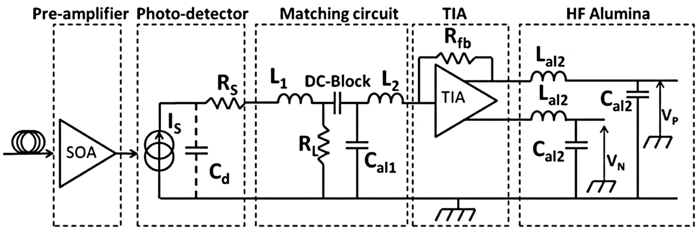
Figure 14 shows the detailed electrical equivalent circuit of the receiver. Each sub-part of this circuit has been modeled using “Advanced Design System” (ADS) software. The equivalent photodiode circuit has been obtained thanks to small signal measurement. The TIA has been represented thanks to an accurate transistor model extracted from measurement. Passive elements, such as the transmission lines, have been designed with the three-dimensional (3D) electromagnetic simulation software “High Frequency Structural Simulator” (HFSS) and imported on ADS in order to be accurately modelized.

Fig. 14. Electrical equivalent circuit.
Two modules have been realized, with and without a matching load. Figure 16 shows the normalized measurement results of both modules, compared with the simulations results. The good agreement between simulations and measurements results allows validating the design methodology. The measured −3 dB bandwidth for both modules, with and without matching load, are 43 and 21 GHz, respectively.
The following measurements relate only to the photoreceiver with matching load (shown in Fig. 15).
Fig. 15. Module photograph.
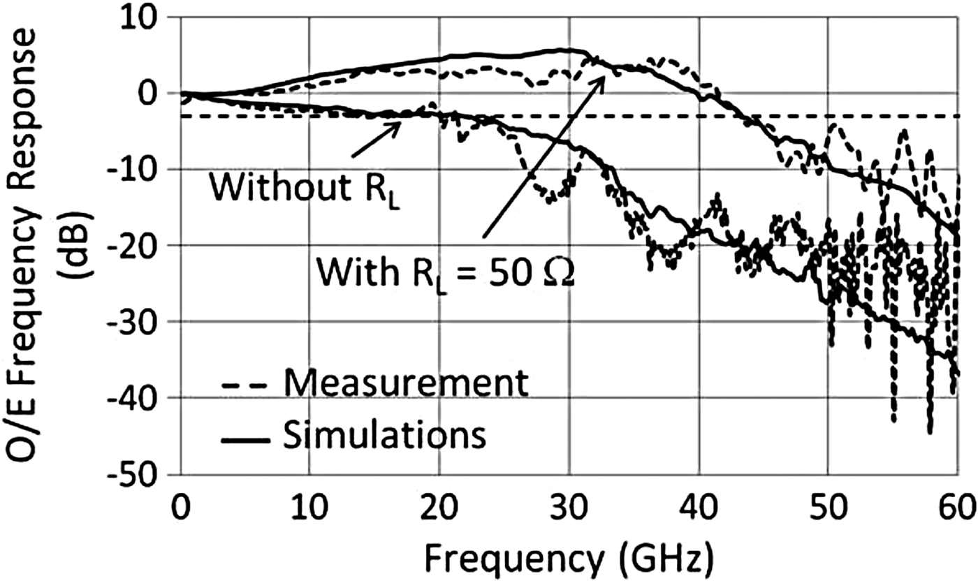
Fig. 16. Normalized opto-electrical frequency response of the photoreceiver modules.
C) Large signal: eye diagram
Figure 17(a) shows the eye diagram at 40 Gb/s with the same exact conditions as the ones used for small signal measurements, with V bw = −3.3 V and V gc = −0.35 V. An overshoot on the eye is observed, which is linked to the peaking effect visible on the O/E response (Fig. 16). By reducing the input stage V bw voltage bias of the TIA, the bandwidth and the peaking effect decrease, so that the overshoot on the eye diagram is removed, as shown in Fig. 17(b). Thus, a perfectly open 40 Gb/s eye is observed. As for the small signal experiment, the large signal simulation results are in a good agreement with the measurement results as plotted in Figs 17(a) and 17(b).
Fig. 17. (a) 40 Gb/s Eye diagram, V bw = −3.3. V (b) 40 Gb/s eye diagram, V bw = −1.8 V (c) Eye amplitude depending on the optical power.
Figure 17(c) shows the single ended eye amplitude versus the optical input power. The linearity of the module conversion gain up to an input optical power of −17 dBm is observed. The conversion gain of the module, calculated from this curve is equal to 10 000 V/W at −25 dBm with an extinction ratio of the optical modulator of 7 dB. The linearity limitation at high-input power is due to a combination of the SOA optical gain saturation and the limitation of the TIA.
D) Bit error rate
The 40 Gb/s back-to-back BER measurements have been performed in Orange Lab (Lannion, France). Measurements at higher bit rates than 40 Gb/s are limited by the optical source.
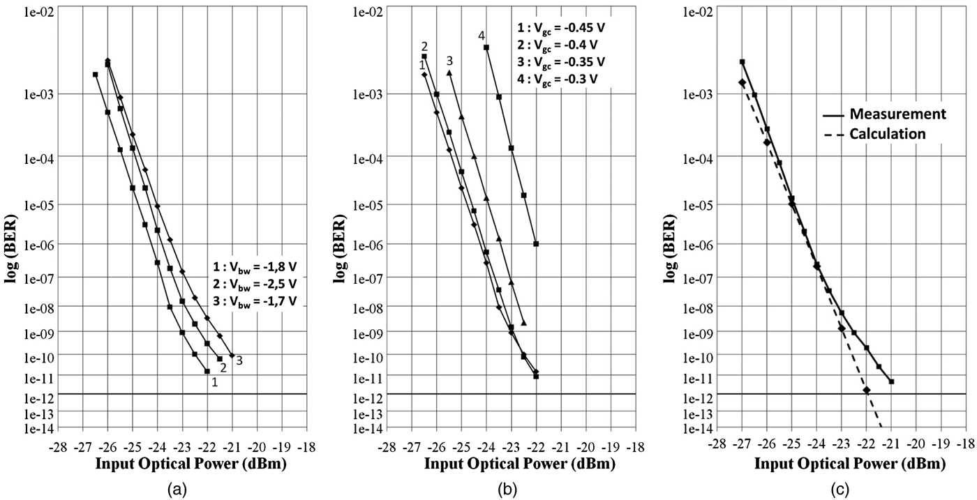
Figure 18(a) shows the effect of the bandwidth control bias voltage V bw on the BER. It has been noted in Section IV.C that a too high value of V bw causes overshoots on the eye diagram because of the peaking effect observed in the frequency domain. By lowering this value, the overall bandwidth is reduced and the overshoots are cancelled. Moreover, the ENB is also reduced. Thus, the overall noise is lowered and the SNR improved. Nevertheless, if V bw is set at a too low value, the photoreceiver bandwidth will not suit 40 Gb/s communication and will lead to a higher number of errors. Moreover, the TIA gain is also affected by V bw and the eye amplitude will be minimized for low-voltage values. Thus, in order to get the lower bit error rate, an optimal value of this bias voltage is obtained for V bw = −1.8 V.
Fig. 18. The 40 Gb/s BER measurements: (a) depending on V bw value at V gc = −0.45 V;, (b) depending on V gc value at V bw = −1.8 V;, and (c) comparison with calculation, V bw = −1.8 V, V gc = −0.45 V.
Figure 18(b) shows the effect of the gain control bias voltage V gc. The input referred noise of the TIA decreases when the gain increases, and then becomes stable for high V gc value. This variation, combined with the evolution of the eye amplitude depending on the V gc value, is directly transcribed on the BER measurement. The BER improves while increasing the magnitude of V gc between −0.3 and −0.4 V. Then, the improvement on the BER between V gc = −0.4 V and V gc = −0.45 V is very low.
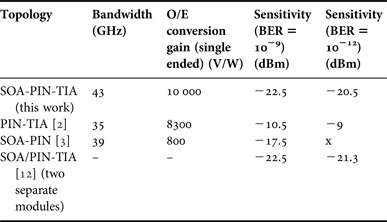
Figure 18(c) shows the high performances of the SOA-PIN–TIA module for an SOA biasing equal to 140 mA. A −22.5 dBm sensitivity has been measured for BER of 10−9. The good agreement between the predicted BER and the measured one, allows validating the design methodology, presented in the appendix. To the best of our knowledge, this represents the highest sensitivity for a pre-amplified monolithically integrated photoreceiver co-packaged with a TIA. Table 1 shows the state of the art of different photoreceiver architectures.
Table 1. State-of-the-art of 40 Gb/s NRZ operating optical receiver.
V. CONCLUSION
We have demonstrated a very high sensitivity (−22.5 dBm at 40 Gb/s for a BER of 10−9), very high-gain (10 000 V/W) and high linearity SOA-PIN–TIA single wavelength photoreceiver module with 43 GHz bandwidth for high-speed PON networks. Its design was conducted thanks to a complete simulation methodology that has allowed an accurate prediction of small and large signal behavior. Its high sensitivity and its low cost could make it a preferred solution for the next PON architecture.
ACKNOWLEDGEMENT
The author wants to thank the Orange Labs Advanced Studies on Home and Access team, especially Philippe Chanclou and Gaël Simon for their welcome and with whom the 40 Gb/s BER measurements have been performed.
Philippe Angelini was born in Tulle, France, in 1989. He received the Master degree in Electronic Engineering from the University of Limoges, Limoges, France, in 2013. In 2013, he joined III-V Lab, Bell Labs, Marcoussis, France, as a Ph.D. student, where he is working on new co-packaging techniques for high-speed opto-eletrical receivers and transmitters.
Fabrice Blache received the Ph.D. degree in Electronics from the University of Limoges, Limoges, France, in 1995. He is currently a research engineer with the III-V Lab, in Marcoussis, France, a joint laboratory of Alcatel-Lucent Bell Labs France, Thales Research and Technology and CEA-Leti, where his main expertises are in the field of high-frequency designs for opto-electronic modules. He is currently leading research activities for 100 Gbit/s applications.
Christophe Caillaud received his Engineer degree in Physics from ESPCI ParisTech, Paris, France, and the Master's degree in Optoelectronics from Ecole Polytechnique, Palaiseau, France, in 2007. He received the Ph.D. degree from Telecom ParisTech, Paris, France, in 2010. During the Ph.D. degree he worked at III-V Lab on high-speed receiver and on the integration of an SOA with a photodiode for 40–100 Gbit/s applications. After the Ph.D. degree, he joined III-V Lab where he is involved with the design, fabrication, and characterization of photonic integrated circuits for 40 and 100 Gbit/s applications.
Michel Goix received the Vocational training certificate in physical measurement in 1979. Between 1980 and 1990 he worked at the Research Central laboratory of Thomson-CSF. He joined Alcatel Alsthom Research in 1991 and Alcatel-Lucent Bell Labs since 2006 where he works as a mechanical designer on packaging process for high bit rate optical transmission modules.
Filipe Jorge was born in Roubaix, France, in 1970. He received the Ph.D. degree in Electronic Engineering from the University of Lille 1, Villeneuve d'Ascq, France, in 1999. In 2000, he joined OPTO, an Alcatel Research and Innovation unit, as a Research and Development Engineer. He is currently involved in module design and characterization of high-speed circuits for optical communication systems with the Alcatel-Thales III-V Lab, Marcoussis, France.
Karim Mekhazni is born in November 1977. He joined III-V Lab, Bell Labs, Marcoussis, France in February 2014 where he works as a technical developer for high-speed components and modules for optical communication systems.
Jean-Yves Dupuy (M'05) received the Electrical Engineering degree from Ecole Nationale Supérieure de l'Electronique et de ses Applications (ENSEA, Cergy, France) in 2005. He joined III-V Lab (Marcoussis, France), in 2005, where he is currently a Research Team Leader. Since 2005 he has been developing very high-speed monolithic microwave-integrated circuits in InP DHBT technology for optical communication systems at 40, 100, and 400 Gb/s. Since 2012, he has also been leading a very high-speed optoelectronic functional packaging effort aiming at pioneering beyond-100-Gb/s optical communication subsystems. His current research interests include very high-speed ICs, modules and sub-systems for next generation optical and wireless communication technologies. He has authored or co-authored more than 50 publications and holds one patent. In 2011, he was granted by the French National Research Agency (ANR) a funding for the collaborative project HENIAC. In 2013, he was selected and invited to the 2013 EU-US Frontiers-Of-Engineering Symposium.
Mohand Achouche is the head of III-V Lab Opto-Electronic Integrated Circuit (OEIC) Department, where he has the highly challenging mission to build the next generation transceivers for telecom and data communication applications, by bringing together high-speed ASICs activities with photonic integrated circuits (PICs). He received a Ph.D. degree from Paris VII (Jussieu) University in 1996. His research activities started in 1993 at the National Centre of Telecommunication Research (CNET, Laboratoire de Bagneux) on the fabrication and characterization of HEMT transistors for high-speed circuits applications. During 1997–2000, he was with Ferdinand Braun Institute (FBH-Berlin) working on power amplifiers based on GaAs HBTs for mobile communications. In 2000, he joined Alcatel Research and Innovation where he was first involved in 40 Gb/s photodiodes. In 2004, he was in charge of a research team on photoreceivers for high-speed optical communication systems, microwave photonics links and sensors. In 2011, he was in charge of Photonic integrated Circuit department working on transmitters and receivers based integrated photonic circuits for core and metro networks.