I. INTRODUCTION
InP-based heterojunction bipolar transistors (HBTs) in transferred substrate (TS) technology have demonstrated excellent high frequency operation with simultaneous high-output power densities [Reference Jensen, Kraemer, Al-Sawaf, Krozer, Heinrich and Traenkle1]. Compared with a conventional triple mesa HBT, the TS technology allows a reduction of the extrinsic parasitic capacitance between the base and collector semiconductor regions of the HBT device. This leads to devices demonstrating extremely high-frequency operation with potential for active electronics in the sub-THz (0.1–1 THz) frequency range [Reference Scott, Monier, Wang, Radisic, Nguyen, Cavus, Deal and G.-Aitken2].
From a modeling point of view the TS-HBT devices are expected to behave quite similar to other III–V based HBTs. In HBTs based on III–V materials the dependence of the electron velocity on electrical field leads to a complicated bias dependence for the cut-off frequency f t and base–collector capacitance C bc [Reference Camnitz and Moll3]. The cut-off frequency is determined from the total emitter–collector delay in the device and is dominated by the collector transit time. Large-signal models for III–V based HBTs, such as the University of California, San Diego (UCSD) HBT model, Ferdinand-Braun-Institut für Höchstfrequenztechnik (FBH) HBT model, and the Agilent HBT model mainly differ in their way of implementing electron velocity modulation effects [Reference Rudolph4]. Another effect often seen in InP-based double HBTs is related to the formation of a barrier for electron flow at the base–collector heterojunction at high collector current levels (collector blocking). Collector blocking manifests itself in the output characteristics as a soft transition between the saturation region and the forward active region (similar to quasi-saturation). For this reason, it is sometimes referred to as the “soft-knee” effect. The UCSD and Agilent HBT models both include parameters to model the “soft-knee” effect but it is not yet implemented in the FBH model. For some III–V based HBTs it has been proven to be necessary to augment the small-signal equivalent circuit model with a capacitor C bi in shunt with the intrinsic base resistance R bi to represent AC-current crowding [Reference Degachi and Ghannouchi5]. This effect has not yet been implemented in any of the large-signal HBT models mentioned above and it remains questionable whether the effect is noticeable in TS-HBTs.
In this paper, the direct extraction of the small-signal equivalent circuit parameters for TS-HBTs in two-terminal and three-terminal configurations is discussed. The direct parameter extraction method is dedicated to III–V based HBTs and unique in the sense that it allows the extrinsic base and emitter access impedances to be extracted without relying on the “open-collector” method [Reference Gobert, Tasker and Bachem6]. This is accomplished by employing a multi-bias extraction procedure similar to [Reference Johansen, Krozer, Nodjiadjim, Konczykowska, Dupuy and Riet7] and by a separation between low and high frequency effects. Thereby it will be shown that the standard “open-collector” measurement step can be significantly simplified as the remaining collector access impedance can be extracted reliably at much lower base currents than the base and emitter access impedances. After the determination of the small-signal equivalent circuit model parameters the ability of the FBH HBT model to predict the large-signal performance of TS-HBTs with good accuracy at millimeter-wave frequencies is demonstrated for the first time.
II. TEST-STRUCTURE LAYOUT AND DE-EMBEDDING
The TS-HBT devices considered in this paper have been developed at the FBH. They feature f t and f max values above 400 GHz [Reference Kraemer, Rudolph, Schmueckle, Wuerfl and Traenkle8]. Two types of the TS-HBT devices were fabricated to allow circuit connections in two-terminal and three-terminal configurations. The two-terminal configuration provides access to the base and collector terminals of the device while the emitter terminal is grounded. For the three-terminal configuration all device terminals are accessible. This makes implementations of common-base and cascode stages possible. Both device types come in single-finger and two-finger versions. Figure 1(a) shows a microphotograph of the on-wafer test-structure for a two-terminal single-finger device with 0.8 × 6−µm2 emitter area. In this device type the emitter is grounded directly underneath the device to reduce the parasitic emitter inductance to a minimum. Part of the ground plane underneath the base terminal line, however, is removed for lower parasitic capacitance which leads to an increase in base access inductance, as will be shown later. The three-terminal device type is also characterized in a common-emitter configuration. However, due to an additional ground plane opening under the emitter of the device the parasitic wiring inductances can become quite large and must also be carefully modeled.

Fig. 1. (a) Microphotography of on-wafer test-structure showing reference planes for model extraction and (b) the corresponding equivalent-circuit model assumed for the de-embedding procedure.
As a model to be used for circuit design should represent the integrated device the reference planes for model extraction are located at the boundary of the device layout cell as shown in Fig. 1(a). The de-embedding of the pads and access micro-strip lines is performed in two steps: at first, an equivalent circuit model for a 420 µm long microstrip line connected with pads at both ends is developed from measured S-parameters. This allows the identification of the equivalent-circuit model shown in Fig. 1(b) representing the pads and access microstrip lines to the device-under-test (DUT). Next the influence from the pads and access microstrip lines is removed from the measured S-parameters of the TS-HBT device.
III. SMALL-SIGNAL EQUIVALENT CIRCUIT MODELING
A) Small-signal model structure
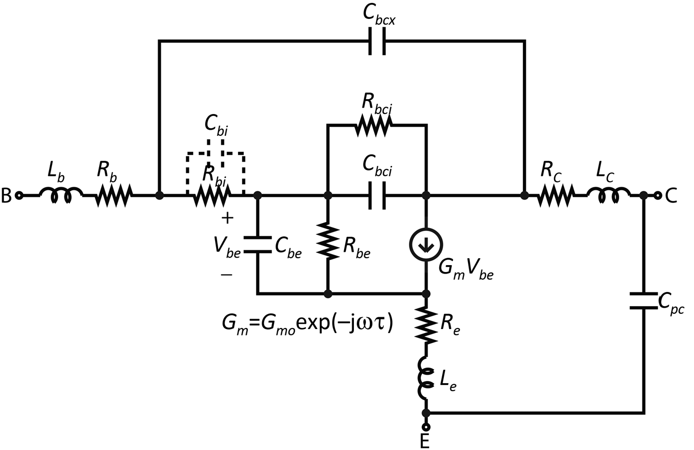
The small-signal model structure proposed for the TS-HBT devices considered in this work is shown in Fig. 2. A hybrid-π small-signal equivalent circuit topology is chosen as it corresponds well to the linearized circuit arising from most large-signal models. A parasitic collector–emitter overlap capacitance C pc is included at the output of the small-signal equivalent circuit model. Due to the opening of the ground plane underneath the base terminal any overlap capacitances between the base–emitter terminals are expected to be of small value. It can therefore be absorbed into the much larger internal base-emitter capacitance C be without any consequence for the model accuracy. In InP-based TS-HBTs a significant part of the total transit-time stems from the collector region and may lead to transcapacitances in a small-signal description of the device [Reference Rudolph4]. In the hybrid-π equivalent circuit model the effect of transcapacitances can be modeled as an equivalent time-delay τ on the transconductance as shown in Fig. 2. For some III–V based HBTs the effect of AC-current crowding is noticeable and needs to be modeled [Reference Degachi and Ghannouchi5]. In this case, the small-signal model structure can be augmented with a capacitance C bi in shunt with the intrinsic base resistance R bi as indicated in Fig. 2.
Fig. 2. Small-signal equivalent circuit model for the TS InP HBT devices. The capacitance C bi is included in the augmented small-signal equivalent circuit model.
B) Direct parameter extraction methodology
The extraction of the elements of the small-signal equivalent circuit model follows an analytical procedure based on the two-port parameters measured in cut-off, open-collector, and forward active biasing modes. The steps in the extraction procedure are described in the following:
1) CUT-OFF MODE EXTRACTION OF OVERLAP CAPACITANCE
Starting from the collector side, the collector–emitter overlap capacitance C pc is first extracted from cut-off mode Y-parameters as 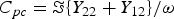 $C_{pc} = \Im \lcub Y_{22} + Y_{12} \rcub /\omega$. Once determined the influence from C pc can be removed from all measured data and will not receive further considerations during the remaining extraction procedure. Despite its small value of around 2–4 fF, failure to perform this step can have a surprisingly large effect on the extraction results described in the following steps.
2) DETERMINATION OF THE DISTRIBUTION FACTOR FOR BASE–COLLECTOR CAPACITANCE
The zero current distribution factor X CJC between the intrinsic and total base-collector capacitance can be determined from Z-parameters in the cut-off mode as
 $$\eqalign{f\lpar X_{CJC} \rpar &= \displaystyle{\Im \lpar Z_{11} - Z_{12}\rpar \Im \lpar Z_{22} - Z_{12} \rpar \over \Re \lpar Z_{12}\rpar ^2} \approx \displaystyle{X_{CJC}^2 \over 1 - X_{CJC}} \Rightarrow \cr X_{CJC} &=\displaystyle{ - f\lpar X_{CJC}\rpar \pm \sqrt{f\lpar X_{CJC}\rpar ^2 + 4f\lpar X_{CJC}\rpar } \over 2}\comma \; }$$
where only the solution giving X CJC between zero and one is valid [Reference Johansen, Krozer, Nodjiadjim, Konczykowska, Dupuy and Riet7]. The approximation leading to (1) comes from neglecting the influence from the yet unknown emitter resistance R e on  $\Re$ (Z 12). The zero current distribution factor is useful for the extraction of the extrinsic base resistance as will be described later. It is also an important parameter in the FBH large-signal HBT model. Figure 3 shows the zero current distribution factor versus frequency extracted from the two-terminal single-finger device at a bias point in the cut-off region. The frequency range for extraction is chosen low enough to neglect the influence from parasitic inductances on the result. An average value of around X CJC ≈ 0.6 is extracted, which corresponds quite well to the calculated ratio of the emitter to collector area in the 0.8 × 6-μm2 InP-based TS-HBT device. The extracted value of X CJC indicates that a significant external base–collector capacitance C bcx is still present in the TS-HBT device despite the effort to reduce the overlap between the base and collector semiconductor regions.
Fig. 3. Zero current distribution factor X CJC between intrinsic and total base collector capacitance versus frequency extracted from the cut-off bias mode.
3) COLLECTOR RESISTANCE AND COLLECTOR INDUCTANCE EXTRACTION
The next step in the procedure is the extraction of the collector resistance R c and collector inductance L c from Z-parameters measured under the open-collector condition. The open-collector method [Reference Gobert, Tasker and Bachem6] is the standard way to extract also the access base and emitter access impedances of HBTs. The method, however, is complicated by a distributed diode between the base and collector. This leads to an underestimation of the external base resistance R b and an overestimation of the emitter resistance R e as discussed in [Reference Johansen, Krozer, Hadziabdic, Jiang, Konczykowska and Dupuy9]. Furthermore, to assure proper convergence of the extracted elements, very large base currents are typically required with high risk for device damage. Figure 4 shows the real and imaginary part of the access impedances extracted for the two-terminal single-finger device at an open-collector bias condition. Here Z 11−Z 12, Z 12, and Z 22−Z 12 corresponds to the access impedance for the base, emitter, and collector terminals, respectively, The base current level of I b = 3 mA represents the limit for safe device operation. The collector resistance and collector inductance is observed to converge to constant values at this base current level, at least up to 40 GHz, whereas no constant inductance can be identified from the base and emitter reactances. The negative slope versus frequency for the emitter access reactance actually indicates a negative inductance which is clearly not physical. Therefore, the open-collector method is found to be useful only for the extraction of the elements associated with the collector access impedance.
Fig. 4. Real (a) and imaginary (b) parts of access impedances versus frequency for the two-terminal single-finger device extracted at the open-collector bias mode.
4) EXTRINSIC BASE RESISTANCE EXTRACTION
To overcome the complications using the open-collector method for extraction of the extrinsic base resistance an alternative approach based on two-port parameters measured in the forward-active mode was recently developed [Reference Johansen, Krozer, Nodjiadjim, Konczykowska, Dupuy and Riet7]. The method exploits the physical behavior of the base–collector capacitance found in III–V based HBTs [Reference Camnitz and Moll3]:
 $$C_{bc} = C_{bc0} - \displaystyle{k_1 I_c \over 2} \left[1 - \displaystyle{I_c \over I_{tc}} \right]\comma$$
where C bc0 is the total base–collector capacitance at zero current, k 1 describes the electron velocity modulation effect due to electric field in the collector, and I tc is a characteristic current describing the response of the electric field to current flow in the collector. Fig. 5(a) plots the base–collector capacitance from (2) versus collector current fitted to experimentally extracted values using 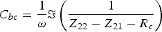 $C_{bc} = \displaystyle{1 \over \omega }\Im \left(\displaystyle{1 \over Z_{22} - Z_{21} - R_c} \right)$. Based on the small-signal equivalent circuit diagram of Fig. 2 an effective base resistance can be defined at lower frequencies as:
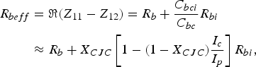 $$\eqalign{R_{beff} &= \Re \lpar Z_{11} - Z_{12} \rpar = R_b + \displaystyle{C_{bci} \over C_{bc}} R_{bi} \cr &\approx R_b + X_{CJC} \left[1 - \lpar 1 - X_{CJC}\rpar \displaystyle{I_c \over I_p} \right]R_{bi}\comma \;}$$
where (2) allows the current-dependent ratio between intrinsic and total base–collector capacitance to be represented by its linear approximation for I c /I p ≪ 1 with I p = 2X CJCC bc0 /k 1. The extracted effective base resistance values extrapolated to the collector current I c = I 0/(1−X CJC) are observed to reduce to the extrinsic base resistance R b as the linear approximation for the current-dependent ratio between intrinsic and total base-collector capacitance reaches zero at this point. Figure 5(b) illustrates the external base resistance extraction method applied to the two-terminal single-finger device.
Fig. 5. (a) Extracted base–collector capacitance versus collector current. The dashed line is the modeled response using (2) with parameters C bc0 = 11.0 fF, k 1 = 0.5 ps/V, and I tc = 45 mA. (b) Effective base resistance plotted versus 1 − (1 − X CJC)I c /I p using parameters X CJC = 0.6 and I p = 26.4 mA. The dashed line is the linear extrapolation for external base resistance extraction.
5) EMITTER RESISTANCE EXTRACTION
The emitter resistance R e can also be extracted from the forward active mode using the method reported in [Reference Rios, Lunardi, Chandrasekhar and Miyamoto10].
6) LOW-FREQUENCY EXTRACTION OF INTRINSIC ELEMENTS
Once the external resistances have been determined their influence is removed from the measured two-port parameters. The remaining elements of the small-signal equivalent circuit model can be determined, e.g. using the method reported in [Reference Suh, Shin, Kim, Heo, Radhavan and Laskar11], by neglecting at first the influence of the base and emitter inductances. This means that the extraction must be performed at low frequencies.
7) HIGH-FREQUENCY EXTRACTION OF EXTRINSIC INDUCTANCES
The base and emitter inductances are extracted from the forward-active region using the elements determined in the previous step as follows
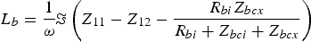 $$L_b = \displaystyle{1 \over \omega} \Im \left(Z_{11} - Z_{12} - \displaystyle{R_{bi} Z_{bcx} \over R_{bi} + Z_{bci} + Z_{bcx}} \right)$$
and
 $$\eqalign{L_e =& \displaystyle{1 \over \omega} \Im \left(Z_{12} - \displaystyle{Z_{be} \over 1 + G_m Z_{be}} \right. \cr - & \left. \,\,\displaystyle{R_{bi} Z_{bci} \over \lpar R_{bi} + Z_{bci} + Z_{bcx}\rpar \lpar 1 + G_m Z_{be}\rpar } \right)\comma \; }$$
where 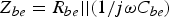 $Z_{be} = R_{be} \vert \vert \displaystyle{\lpar1 / j\omega C_{be}\rpar}$,
  $Z_{bci} = R_{bci} \vert \vert \displaystyle{\lpar1 / j\omega C_{bci}\rpar}$, and
 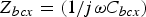 $Z_{bcx} = \displaystyle{\lpar1 / j\omega C_{bcx}\rpar}$. A similar approach was followed in [Reference Horng, Wu and Huang12]. Figures 6(a) and 6(b) illustrate the extraction of the base and emitter inductances applied to two-terminal and three-terminal single-finger devices, respectively. The extraction is performed in the frequency range from 50 to 65 GHz, where the values show the least dispersive behavior. A rather large base terminal inductance in the range of 8–12 pH is extracted for the two-terminal single-finger device. It has been verified by electromagnetic simulations that this is caused by the opening of the ground plane underneath the base line. For the three-terminal device an even larger base terminal inductance around 18–22 pH is extracted. The extracted emitter terminal inductance around 18 pH for the three-terminal device is also quite large. The larger terminal inductances for this device type is a consequence of its more open layout structure necessary to provide external connections to all three device terminals. It may be necessary to iterate between steps 6) and 7) as the terminal inductances influence the extracted values of the intrinsic elements. The terminal inductances for both device types are quite large and expected to have a significant influence on the performance of millimeter-wave circuits.
Fig. 6. Extraction of base and emitter inductances for (a) two-terminal single-finger device and (b) three-terminal single-finger device in the frequency range from 50 GHz to 65 GHz.
C) Extraction results and discussion
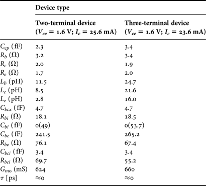
The small-signal equivalent circuit elements for the two-terminal and three-terminal single-finger devices found from the direct parameter extraction methodology are provided in Table 1. A good consistency is observed between the two small-signal equivalent circuit models in the sense that it is mainly the external reactive elements that differ. The time-delay τ on the transconductance describing non-quasi-static effects has a minor influence on the S-parameters making it difficult to extract a reliable value from experimental data. It is therefore fixed at zero in the small-signal equivalent circuit model. Figure 7 shows a comparison between the measured and simulated S-parameters for the two-terminal single-finger device using these extracted elements. The S-parameters have been de-embedded to reveal more details about the modeling of the device structures. In general, the simulation with the small-signal model matches the measured data well but a slight deviation is observed in S 11 above approximately 58 GHz. Whether this deviation is caused by the lack of AC current crowding modeling or by measurement inaccuracies is hard to assess. However, by assigning the physical plausible value of (C be + C bc)/5 to the intrinsic base capacitance C bi the match between measured data and simulated response is clearly improved as observed in Fig. 7. This value follows from an approximate lumped representation of the distributed RC network in the lateral direction along the intrinsic base [Reference Versleijen13]. Figure 7 also shows a deviation between measured and simulated responses for S 12. As observed, this deviation cannot be explained by the proposed AC current crowding modeling. Instead it is found that the deviation is caused by an abrupt drop in the phase of S 12 above 74 GHz. There are no elements of the small-signal equivalent circuit model that can be used to explain such an abrupt phase change and hence the deviation must be attributed to a measurement artifact. The comparison between the measured and simulated S-parameters for the three-terminal single-finger device is shown in Fig. 8. Again a good match between simulated and measured S-parameters is observed. The augmented small-signal model seems to improve the match to measured data for this device type also.
Fig. 7. S-parameters of two-terminal single-finger device from 50 MHz–110 GHz. The figure compares measurements (solid line) with small-signal model response (solid line with circles), and augmented small-signal model response (solid line with squares). The bias point is at V ce = 1.6 V; I c = 25.6 mA.
Fig. 8. S-parameters of three-terminal single-finger device from 50 MHz–110 GHz. The figure compares measurements (solid line) with small-signal model response (solid line with circles), and augmented small-signal model response (solid line with squares). The bias point is at V ce = 1.6 V; I c = 23.6 mA.
Table 1. Small-signal equivalent circuit elements for two-terminal and three-terminal single-finger devices. The value used for C bi in the augmented small-signal equivalent circuit model is given in parenthesis.
IV. LARGE-SIGNAL MODELING
The large-signal modeling of the TS-HBTs is based on the FBH HBT model formulation. The FBH HBT model was originally developed for GaAs HBTs but should be versatile enough to model also InP-based HBTs [Reference Rudolph4]. After transferring the elements found from small-signal extraction to the large-signal model, the parameters affecting the DC and thermal characteristics of the device are determined. The forward output characteristics presented in Fig. 9 show a quite different behavior compared to GaAs HBT devices. This is caused by an almost temperature independent forward current gain βf typically found in InP-based HBTs. The forward output characteristic is modeled with reasonable accuracy even though the “soft-knee” effect caused by collector blocking (or quasi-saturation) is neglected so far by the FBH HBT model. As mentioned in the introduction, III–V based HBTs experience electron velocity modulating effects affecting both the base–collector capacitance and transit time. The FBH HBT model implements these effects through an unified collector charge [Reference Rudolph4]. The model parameters used to describe this collector charge are determined from the base–collector capacitance and cut-off frequency versus current extracted at different collector–emitter voltages. Despite the rather limited number of model parameters available to describe the collector charge it is found that the bias dependence of the small-signal parameters is well modeled. The onset of base push-out is controlled by the current I ck with the asymptotes defined as I c = (V ce − V ces)/R ci0 and I c = I k + (V ce − V ces)/R jk where V ces, R ci0, I k, and R jk are model parameters. These asymptotes are indicated in the output characteristics of Fig. 9. As a possible work-around for the lack of “soft-knee” effect modeling we propose to adjust the model parameters R ci0 and V ces to limit the RF signal swing into the “soft-knee” region. In this way, the model will limit any signal swing into this region through a sharp increase in the transit-time and base-collector capacitance. This is illustrated in Fig. 9 by the superimposed dynamic load line for 1 dB gain compression at 77 GHz with a 50 Ω load.
Fig. 9. Measured (solid line w. symbols) and modeled (solid line w.o. symbols) forward output characteristics for two-terminal single-finger device. The base current is varied from 0.05 to 0.6 mA in steps of 0.05 mA. The dashed lines indicate chosen asymptotes for the onset of base push-out in the model. The dynamic load line for 1 dB gain compression at 77 GHz with a 50 Ω load is superimposed on the forward output characteristics.
For verification of the developed TS-HBT large-signal model at millimeter-wave frequencies, the large-signal performance in a 50 Ω setup was measured using a 77 GHz Gunn source followed by an E-band attenuator. Input powers up to +10 dBm are possible with this setup. As seen in Fig. 10(a) the large-signal model is able to accurately predict the output power and gain compression characteristics for the two-terminal single-finger device even at the highest input power levels. This indicates that the base push-out parameter extraction approach proposed here for the FBH HBT model may be sufficient to model the “soft-knee” effect for practical purposes. Therefore, it does not seem strictly necessary to augment the model with a description of the “soft-knee” effect in order to better capture the characteristic of the InP-based TS-HBTs. To illustrate the scalability of the developed large-signal model Fig. 10(b) shows the large-signal performance for a two-finger device in two-terminal configuration. As the two emitter fingers in this device share the same mesa structure the external reactive elements are kept constant in the scalable model. The model's current and capacitance parameters are assumed to scale proportional with the number of fingers while resistances scale inversely proportional in line with the general scaling rules for the FBH HBT model [Reference Rudolph4]. The excellent prediction of the output power and gain compression characteristics seen in Fig. 10(b) verifies this modeling approach.
Fig. 10. Measured (solid line w. symbols) and simulated (solid line) large-signal performance at 77 GHz for (a) single-finger device biased at V ce = 1.4 V with a quiescent current of I cq = 22.7 mA and (b) two-finger device biased at V ce = 1.4 V with a quiescent current of I cq = 29.6 mA.
V. CONCLUSIONS
In this paper, the modeling of InP-based HBTs in TS technology is presented. The small-signal equivalent circuit parameters for TS-HBTs in two-terminal and three-terminal configurations are extracted by means of an analytical procedure. The small-signal model structure augmented with an AC current crowding description is shown to improve the match to the measured S-parameters at the highest frequencies. A developed large-signal model based on the FBH HBT model formulation, implemented without AC current crowding and “soft-knee” effects, provides good accuracy for both single-finger and two-finger TS HBT devices, even at millimeter-wave frequencies.
 Tom K. Johansen received his M.S and Ph.D. degrees in electrical engineering from the Technical University of Denmark, Denmark, in 1999 and 2003, respectively. In 1999 he joined the Electromagnetic Systems group, DTU Elektro, Technical University ofDenmark, Denmark, where he is currently an Associate Professor. From September 2001 to Marts 2002 he was a Visiting scholar at the center for wireless communication, University of San Diego, California, Ca. From November 2012 to February 2013 he spent asabbatical at the Ferdinand Braun Institute (FBH), in Berlin, Germany. His research areas include the modeling of HBT devices, millimeter-wave and sub-millimeter-wave integrated circuit design.
 Matthias Rudolph received the Dipl.-Ing. in EE from Berlin Institute of Technology in 1996, and the Dr.-Ing. from Darmstadt University of Technology in 2001. 1996-2009 he was with the Ferdinand-Braun-Institut, Leibniz-Institut für H—chstfrequenztechnik in Berlin, where he was resposible for the modeling of III-V transistors and eventually heading the low-noise components group. Since 2009, he is the Ulrich-L.-Rohde professor for RF and microwave techniques at Brandenburg University of Technology, Cottbus, Germany.
Prof. Rudolph is the Conference software officer of EuMA since 2010, he was chair of the German Microwave Conference 2010, programme chair of EuMW 2007, and EuMW electronic submissions chair 2010 to present. He authored or editored three books and is the author of about 50 reviewed conference and journal papers. In summer 2013, Prof. Rudolph started growing a beard.
Thomas Jensen received the M.Sc and Ph.D degrees from the Technical University of Denmark in 2005 and 2010 respectively. He has been involved in radiometer instrument design, vital signs radar, and THz imaging systems. Currently he is actively engaged in design and measurement of InP HBT circuits and circuit elements at sub-THz frequencies.
 Nils Weimann received the Diploma in physics in 1996 from Stuttgart University, Germany, and the Ph.D. in Electrical Engineering in 1999 from Cornell University, Ithaca, NY, USA. Then he worked at Bell Laboratories in Murray Hill, NJ. He joined Ferdinand-Braun-Institute, Berlin, Germany in 2012 to research InP Terahertz devices and circuits.
 Frank Schnieder received the Dipl.-Ing. and Dr.-Ing. degrees in electrical engineering from the Technical University of Dresden, Dresden, Germany, in 1986 and 1990, respectively. Since 1989, he has been involved with GaAs and GaN devices. In 1992, he joined the Ferdinand-Braun-Institut, Leibniz Institut für H—chstfrequenz-technik (FBH), Berlin, Germany. His current research is focused on device modeling.
 Viktor Krozer received the Dipl.-Ing. and Dr.-Ing. degree in electrical engineering at the Technical University Darmstadt in 1984 and in 1991, respectively. In 1991 he became senior scientist at the TU Darmstadt working on high-temperature microwave devices and circuits and submillimeter-wave electronics. From 1996–2002 Dr. Krozer was professor at the Technical University of Chemnitz, Germany. From 2002-2009 Dr. Krozer has been professor at Electromagnetic Systems, DTU Elektro, Technical University of Denmark, and was heading the Microwave Technology Group. Since 2009 Dr. Krozer is the endowed Oerlikon-Leibniz-Goethe professor for Terahertz Photonics at the Johann Wolfgang Goethe University Frankfurt, Germany. His research areas include terahertz electronics, MMIC, nonlinear circuit analysis and design, device modelling, and remote sensing instrumentation.
 Wolfgang Heinrich received his diploma in electrical engineering, the PhD (Dr.-Ing.), and the Habilitation degree from the Technical University of Darmstadt, Germany. Since 1993, he has been with the Ferdinand-Braun-Institut (FBH) at Berlin, Germany, where he is head of the microwave department and deputy director of the institute. Since 2008, he is also professor at the Technical University of Berlin. His present research activities focus on MMIC design with emphasis on GaN power amplifiers, mm-wave integrated circuits and packaging, and electromagnetic simulation.