I. INTRODUCTION
A number of papers have appeared in the literature on bandwidth enhancement of microstrip antennas. Electrically thick elements, stacked multi-patch, or multi-layer antennas and the impedance-matching network are some of the methods that modify the resonant circuit by adding parasitic patches on top of the original patch, adding gap-coupled patches to the radiating or non-radiating edges. A better way to improve the narrow bandwidth of the conventional patch antenna involves adapting the input impedance knowing that the bandwidth of the radiation pattern is higher than that of the input impedance, i.e. the limiting bandwidth of the microstrip antenna comes from the input impedance. This can be done with a conventional impedance match circuit network or adding parasitic elements electromagnetically coupled to the driven patch. Thus, the additional resonant frequencies are introduced and the magnitude of the reflection coefficient can be kept under a certain level over a wider bandwidth. Parasitic elements can be placed coplanar to the driven patch in different configurations or stacked. The later configuration has been chosen for array elements [Reference Aberle, Pozar and Manges1–Reference Garg, Bhartia, Bahl and Ittipiboon2]. For some applications, single-element antennas are unable to meet the gain or radiation pattern requirements. Combining several single antenna elements in an array can be a possible solution. Antennas exhibit a specific radiation pattern. The overall radiation pattern changes when several antenna elements are combined in an array. The overall radiation pattern results in a certain directivity and thus gain linked through the efficiency with the directivity. The bandwidth of the microstrip antenna can be increased using various techniques such as by loading a patch, using a thicker substrate, by reducing the dielectric constant, using gap-coupled multi-resonator, etc. However, using a thicker substrate cause's generation of spurious radiation. The spurious radiation degrades the antenna parameters. Among the various antenna bandwidth enhancement configurations, the gap-coupled circular microstrip antenna is the elegant one and is a suitable method for enhancing the impedance bandwidth of the antennas. This technique utilizes mutual coupling for achieving wide band along with good impedance matching. With proper optimization of antenna elements, the antenna radiation characteristics can also be improved to a good extent including directivity, side lobe level. Also this technique reduces the fabrication cost with increased efficiency. In the configuration of gap-coupled microstrip antennas method, patches are placed close to each other. The gap-coupled microstrip antennas generate two resonant frequencies and the bandwidth of the microstrip antennas can be increased [Reference Khare and Nema3–Reference Vaidya, Gupta, Mishra and Mukherjee11]. A circuital method for admittance calculation of gap-coupled sectoral patch is also presented earlier in [Reference Kandwal, Chakravarty and Khah6]. In [Reference Kandwal, Chakravarty and Khah6], it is shown that how gap coupling results in bandwidth enhancement with perfect impedance matching. A numerical approach has also been presented in order to provide result comparison with the experimentally measured results.
In this work, we have investigated a wideband gap-coupled sectoral patch antenna array with high directivity along with low side lobe level. At higher frequencies such as in X-band, it is difficult to obtain wide impedance bandwidth along with good radiation properties and a very few papers are there in the literature. This paper proposed a simple and efficient antenna array design using gap coupling to obtain these properties. The antenna proposed has been studied with different gaps between the circular patches and sectoral antennas. A parametric study has thus been presented to find the optimal values of the antenna geometrical parameters. Simulation and experimental studies are then performed to understand the broadband mechanism of closely spaced elements. Effect of element spacing and mutual coupling on the proposed antenna design has been studied and a comparison with results in the literature is therefore presented with the help of results obtained.
II. ARRAY ELEMENT SPACING AND MUTUAL COUPLING
The element spacing has a large influence on the array factor as well. Larger element spacing results in a higher directivity. However, the element spacing is generally kept smaller than λ/2 to avoid the occurrence of grating lobes. Mutual coupling between antenna elements is an important issue in the designing of antenna arrays. It significantly affects the antenna gain, directivity, and beam width of the antenna array. Ludwig studied the relationship of the mutual coupling, antenna gain, and directivity of an antenna array of two identical antennas [Reference Ludwig12] and pointed out there is an optimum non-zero value of mutual coupling and passive reflection coefficient, which yields the maximum array gain. Therefore, mutual coupling can be utilized to achieve bandwidth enhancement with desired performance of reflection coefficient and realized gain by cancelling the reflected waves from each element to the feeding network. Because printed slot antennas are promising candidate used in phased arrays, satellite communication systems and airborne applications due to their compact size and high efficiency, two and four element slot arrays are used to study their mutual coupling and to demonstrate the bandwidth enhancement by invoking suitable mutual coupling [Reference Pozar13–Reference Agrawal, Singhal and Jain16]. Mutual coupling between array elements affects both the embedded element radiation patterns and the element input impedances. The radiation from one driven element induces currents on other nearby elements and scatters into the far field, which causes the embedded element pattern to differ from the isolated element pattern. The driven element also induces a non-zero voltage at the terminals of the other elements. As a consequence, some of the power accepted by the input port of one element is fed as a reverse wave back into the feeding transmission lines connected to other element ports instead of radiating to the far field. These two effects, perturbation of the element patterns and element feed port coupling, are closely related, since the induced voltage at the element terminals. The first effect, scattering from nearby elements is already incorporated into the definition of the embedded element patterns. The second effect, coupling between element ports, can be modeled using microwave network theory.
III. ANTENNA DESIGN
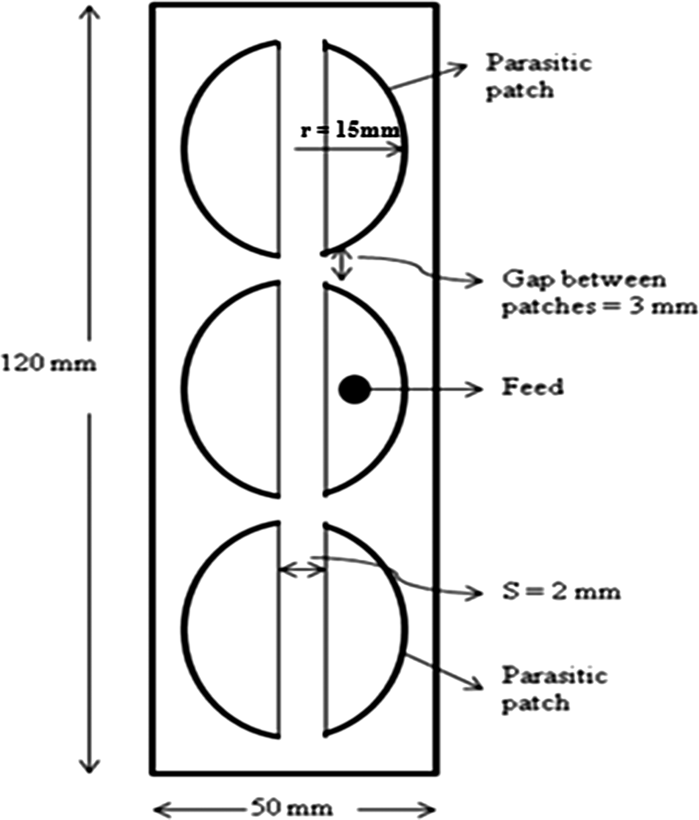
The basic geometry of gap-coupled sectoral patch antenna array is shown in Fig. 1. The antenna array consists of three elements. Out of these three array elements, only one element is excited with a coaxial feed. The other two sectoral antenna array elements act as parasitic elements. The dimension of the antenna design is (120 × 50) mm2. The substrate or dielectric material used is FR4 substrate with permittivity of 4.1 and a loss tangent of 0.024. The thickness of the dielectric substrate used is h = 1.59 mm. The circular patch antenna is of radius r = 15 mm and is fed coaxially at 7 mm in order to achieve 50 Ω characteristic impedance.

Fig. 1. Geometry of antenna structure.
All the three array elements are same placed at a gap of s = 3 mm each. A gap of 2 mm is introduced so as to divide the circular patch antenna into sectoral antenna having two sector patches as shown in Fig. 1.
The prototype of the antenna for experimental measurement is therefore shown in Fig. 2. Figure 2(a) shows the front or top view of the prototype antenna and Fig. 2(b) shows the bottom view of the prototype antenna.
Fig. 2. Prototype of the antenna design. (a) Top view. (b) Bottom view.
IV. MEASUREMENTS AND RESULTS
The results for sectoral patch antenna array with gap coupling using parasitic patches have been compared both through simulations and experimental measurements. The proposed antenna array structure design has been simulated using simulation software CST Studio Suite as well as HFSS and experimentally tested using R & S Vector Network Analyzer. The parameters calculated through simulations and measurements are therefore shown and discussed in following sub sections.
1. S-parameters measurements
2. Input impedance measurements
3. Voltage standing wave ratio (VSWR) measurements
4. Radiation pattern.
A) S-Parameters measurements
The S-parameters or return loss is calculated both through simulations as well as experimental measurements using simulation software and vector network analyzer. The antenna resonates in the X-band within frequency range 8–12 GHz. The result for return loss is shown in Fig. 3. In Figure 3(a), the antenna is studied by varying patch gap to 2 and 4 mm keeping sector gap at 2 mm. In case of patch gap at 2 mm, the maximum return loss obtained is −45 dB with an impedance bandwidth of about 4.8%. When the gap between patches is increased to 4 mm, the return loss obtained is −53 dB with a bandwidth of 4.5%. Likewise, the antenna is studied by varying the sectoral gap keeping the patch gap at 3 mm. Figure 3(b) shows the graph for sector gap at 1 and 3 mm, respectively. The bandwidth obtained at 1 mm gap is about 3.8% with a return loss of −19 dB. As the gap increased to 3 mm, the return loss is −31 dB with a bandwidth of 6.7%. Now the gap between the patches is kept at 3 mm and the gap between the sectors is kept at 2 mm. As can be seen from the results shown in Fig. 3(c), the antenna is resonating at frequency 10.5 and 11.3 GHz. A wide matched impedance bandwidth of about 1 GHz is obtained in this frequency band from frequency 10.3–11.3 GHz. A very good return loss of −50 dB is obtained for the proposed antenna design at the resonant frequency. So, the parametric study reveals that the best results obtained from Fig. 3(c). The simulated and experimentally measured results are in good agreement with each other. A dual resonance is obtained at the two resonant frequencies. This is because the different resonant modes combine resulting in a broadband. The effect of mutual coupling and array element spacing is therefore discussed in the earlier section. The mechanism of parasitic coupling for wide bandwidth is as follows. A parasitic patch placed close to the fed patch is excited through the coupling between the two patches. If the resonant frequencies of the patches (when isolated) are close to each other, then broad bandwidth is obtained, as shown in Fig. 3. The overall input VSWR will be the superposition of the responses of the two resonators resulting in a wide bandwidth. Here also in our proposed gap-coupled sectoral patch antenna array, wider impedance has been obtained due to the combination of the two resonant frequencies. Also the return loss is very less that is −50 dB, which means that the maximum transmission has occurred.
Fig. 3. S-parameters (S11 in dB) or Return Loss variation with frequency (GHz). (a) Patch gap = 2 mm & 4 mm with sector gap = 2 mm. (b) Sector gap = 1 mm & 3 mm with patch gap = 3 mm. (c) Patch gap = 3 mm & sector gap = 2 mm.
B) Input impedance measurements
Input impedance measurements for patch gap at 3 mm and sector gap at 2 mm are shown in Fig. 4(a). The gap between the two patches controls the size of the impedance loop. As the gap increases, the gap coupling decreases and therefore the loop size decreases. Maximum bandwidth is obtained when the loop in the impedance plot is completely inside the VSWR = 2 and its size is as large as possible. In order to achieve a characteristic impedance of 50 Ω, the proposed antenna design structure is thus fed coaxially at one of the sectoral patches. Out of three patches, one is driven element keeping other two as parasitic sectoral patches. The result shows a good impedance matching at the resonant frequency and over the entire resonant frequency band. The simulated results are in good agreement with experimentally measured results.
Fig. 4. (a) Input impedance (Z11 in Ω) variation with frequency (GHz). (b) VSWR variation with frequency (GHz).
C) VSWR measurements
Figure 4(b) reports the VSWR calculated from simulated and experimental results for the proposed gap-coupled sectoral patch array antenna. For entire bandwidth, the VSWR is reported ≤2. From this graph, the impedance bandwidth calculated is about 1 GHz in the X-band.
D) Radiation pattern
The simulated radiation pattern at the resonant frequency is shown in Fig. 5. The effects of adding one parasitic element to the fed patch give rise to asymmetry in the radiation patterns. To compensate the effect of radiation pattern asymmetry, two identical parasitic patches can be used. These can be placed along the radiating edges of the fed patch. In this arrangement, both the parasitic patches are on the opposite sides of the fed patch, one patch will shift the beam maxima in the theta (+) direction, while the other patch will shift it in the theta (−) direction. The overall radiation pattern of the three patches will be the superposition of the individual pattern, and hence will remain symmetrical with broadside direction.
Fig. 5. Radiation pattern for frequency (F) between theta/degree versus dBi. (a) F = 10.46 GHz. (b) F = 10.9 GHz. (c) F = 10.5 GHz.
The polar plots at the resonant frequency of 10.46, 10.9, and 10.5 GHz for directivity (ϕ = 90) between theta/degree versus dBi are shown in the Figs 5(a)– 5(c), respectively. At resonant frequency 10.46 GHz, directivity obtained is 7.4 dBi with a side lobe level of −14.6 dB as shown in Fig. 5(a). In Fig. 5(b) at frequency 10.9 GHz, the directivity is about 8.1 dBi. Within 3 dB angular width in the direction of 43.3°, the side lobe level is about −12.9 dB. Figure 5(c) shows the radiation pattern at the resonant frequency 10.5 GHz. The main lobe magnitude is 11.1 dBi in the main lobe direction 0.0°. For 3 dB angular width, the side lobe level obtained is −23.7 dB in the direction 61.7°. For better antenna radiation, the antenna should have good antenna gain and sufficiently reduced side lobe level.
It is also noted that there is an effect on the impedance when adding an identical parasitic patch to the configuration. The loop size is larger as compared to the two-coupled patch structure configuration. This is due to the fact that the two identical parasitic patches are resonant at the same frequency and hence the coupling increases. To counter balance this effect, one can increase the gap between the fed and the parasitic patches. Coupling along the non-radiating edges of fed patch has similar effects as the coupling along the radiating edges. But it must be noted that the effects are smaller as compared to those from coupling along radiating edges because the field varies sinusoidal along the non-radiating edges. Here in our proposed antenna structure of gap-coupled sectoral patch antenna array, the antenna has a good directivity of 11.1 dBi and the side lobe level is also reduced to a very good extent. The effect of number of elements with the array element spacing is therefore discussed in the previous section. As discussed earlier, the array directivity increases with the number of elements in the antenna array design. The element spacing has been greatly influenced by the array factor as well. Larger element spacing results in a higher directivity. However, the element spacing is generally kept smaller than λ/2 in order to avoid the occurrence of grating lobes. In the proposed design, the element spacing is kept smaller than λ/2. Mutual coupling between antenna elements is an important issue in the designing of antenna arrays. It significantly affects the antenna gain, directivity and beam width of the antenna array. Mutual coupling between array elements affects both the embedded element radiation patterns and the element input impedances. The radiation from one driven element induces currents on other nearby elements and scatters into the far field, which causes the embedded element pattern to differ from the isolated element pattern.
Therefore, we can observe from above results and measurements that the proposed sectoral patch antenna array using parasitic elements is giving very good results in X-band. The antenna has shown wide impedance bandwidth with increased gain and reduced side lobe level to a very good extent.
V. CONCLUSION
A novel concept of using parasitic elements for implementing sectoral patch antenna array for X-band wireless applications has been successfully implemented in this communication. This communication has presented a novel array design in which mutual coupling is thus utilized in order to achieve wide impedance bandwidth along with good directivity and reduced side lobe level. The proposed antenna design works in X-band having a broad matched impedance bandwidth with high antenna directivity along with reduced side lobe level. This antenna is applicable for high-frequency and X-band applications such as radar applications. This paper study reveals that gap-coupled parasitic elements provide a notable broad band and high directivity with the advantage of being low profile, low fabrication cost, small size, and highly efficient.
Mr. Abhishek Kandwal received his M.Sc. degree in Physics from Himachal Pradesh University, Shimla, India, in the year 2009. He is presently pursuing Ph.D. His work includes the design and numerical modeling of wideband microstrip antennas. His field of interest includes designing and developing new numerical methods for wideband microstrip antennas for communication systems.
 Prof. Sunil Kumar Khah received B.Sc. (Electronic Sciences) from Kashmir University; M.Sc., M.Phil, and Ph.D. from Agra University. He did his postdoctoral research in the field of high power microwave component design. Presently, he is working as a professor in the field of Electromagnetics at Department of Physics, Jaypee University of Information Technology. Moreover, he is working on high efficiency low sidelobe level antenna design and wideband dual band antenna designs. His research interest is numerical modeling of high frequency antenna designs. He is life member of PSSI, MRSI, and member of IEEE. Currently, he is visiting researcher at University of Dayton, USA.