I. INTRODUCTION
In 2006, gallium nitride (GaN) technology has made a remarkable breakthrough in the world of microwave electronics with the announcement of commercially available transistors from 5 to 180 W at microwave frequencies. Provided by a major industrial transistor vendor in Japan, but also from US and Europe, equipment manufacturers and in particular those related to space applications now strongly believe that time has come for a rapid insertion of this new technology into their systems.
It is well known that space is a harsh environment. Even inside satellites, equipment is there exposed to severe radiations and sharp temperature variations over a wide range (typ.−55°C/ + 65°C). Also, a successful design should decrease size and weight to a minimum, save a maximum of electrical power and ensure a long lifetime without failure (>15 years for a geostationary satellite). And keep cost to a competitive value despite the fact that manufactured units number is desperately low.
Apart from still to be resolved reliability concerns, these GaN power transistors will increase power density by more than an order of magnitude for large devices, as illustrated in Fig. 1 compared to traditional technologies.

Fig. 1. Reported RF output power density performance for GaN and GaAs transistor (ESA IPC source2006) [1].
Therefore a reduction of size is promised for future module. There is the need for very demanding performance in space industry. A Ku-band (14 to 12 GHz) telecom repeater for instance presents a typical 130 dB gain, 1.1 dB noise figure (at ambient T° at the receiver input), 250 W transmitted power (with 70% power added efficiency (PAE) for the power stage) and high linearity (C/I 3 > 60 dB at receiver output) among the main specifications.
GaN technology features several characteristics that make it an almost ideal candidate for several applications on board satellite payloads.
II. GaN APPLICATIONS
Basically, satellites are used for telecommunication, localization and navigation, earth observation, or planetary exploration. We will focus on few examples.
A) Solid state power amplifiers (SSPA)
At first glance GaN transistors offer significant advantage in terms of achievable power density, while promising a high frequency of operation as any HEMT technology [Reference Inoue2]. This is enhanced by their ability to work at high drain voltage, a perfect request for satellite whose primary bus voltages is typically 100 V. Better DC/DC converter efficiency than today (GaAs PHEMT or HBT are biased around 10–20 V) is expected. It is probably too early to affirm that this solid state will compete with vacuum technology because TWTAs possess an impressive advance in term of PAE, especially under multi-carrier operation. For example, they exceed 68% PAE at Ku-band for a 220 W output and such a performance seems out of reach today. However, the competition is not over at lower frequencies, where lower levels are required and where the situation is already disputed today with GaAs-based SSPA. GaN, allowing higher delivered power in a compact size, may kill the debate. The 120 W L-band necessary, for a Galileo-like navigation satellite, or the 80 W C-band, for future fixed service satellite communication payload, seem perfect targets for GaN insertion.
1) HIGH POWER AMPLIFIER (HPA) MODULES
GaN transistors offer matching aptitude due to a higher output impedance as they work with high voltage, but another characteristic presents significant breakthrough: a high sustainable temperature. This is really the most important benefit. Junction temperature is a very stringent constraint on satellite units design. This is even more pronounced when size is restricted because heat dissipation is even more problematic, like for the power module of an active antenna. Because GaN transistors will not be limited to the normative 115°c junction temperature, they now appear like the technology that system designers were expecting to make transmit active antennae really affordable. A concern will be how low level electronics, passives, etc., behave at high temperature; however, progress is expected here. Faced with that fast-growing technology, different HPAs have been designed. The topology of HPA is based on one stage with one transistor. The HPA (Fig. 2) has been designed in a test fixture integrating input/output matching networks, the transistor, and the RF/DC access. The general performance includes the losses due to the test fixture: the connections and the RF transitions. In a SSPA these losses do not exist and therefore it offers better performances than the one described in this paper.

Fig. 2. Test fixture of HPA 10 W (left side) and 150 W(right side).
Power measurements have been executed (load pull measurements) in order to know the different impedances to put in front of the transistor (see Fig. 3).

Fig. 3. Optimization of fundamental Zload for PAE at Vds = 50 V, f0 = 2.5 GHz.
The PAE is maximum when the fundamental load impedance is fixed at Zopt_Pout_f0 = 7 + j13 Ω. As shown in Fig. 4, the measurement has underlined a sensitivity of transistor performance for the second harmonic concerning the optimum PAE search.
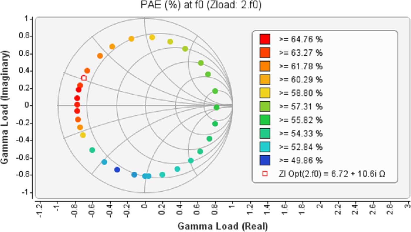
Fig. 4. Optimization of second harmonic Zload.
Concerning the second harmonic, the PAE is maximum when the second harmonic load impedance is fixed at Zopt_2f0 = 6.7 + j11 Ω. Therefore with the same fundamental load impedance, second harmonic optimization allows to add eight points for the PAE. Electrical validation measurement has been performed and allows to characterize the design in:
– small signal: S-parameters;
– power: gain, AM/AM, AM/PM, PAE; and
– linearity: C/I 3.
As shown in the following bench photograph (Fig. 5), the test fixture used an aluminum board with a cooling circuit.

Fig. 5. Picture of measurement bench.
2) HPA 10 W
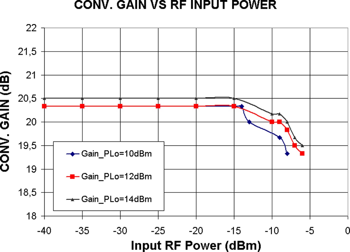
The next results (Fig. 6) confirm the good working of the HPA on a bandwidth of more than 200 MHz around 2.6 GHz and with a linear associated gain more than 15.5 dB. The amplifier is unconditionally stable (K > 1) and the results between 2.5 and 2.7 GHz are:
– S21 ≥ 15.5 dB,
– S11 ≤ −11.5 dB, and
– S22 ≤ −5 dB.

Fig. 6. Measurement of the low level gain of the HPA 10 W.
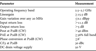
Therefore, the HPA provides an output power level higher than 10 W with an associated PAE of 56% on a bandwidth between 2.5 and 2.7 GHz. The set of points reported in Fig. 7 represents the HPA performance for an input power at 2 dB gain compression. The measurement in Fig. 8 shows a good linearity. Thus, the HPA introduces a C/I 3 level of 30 dBc at 2 dB gain compression. As described in Table 1, this GaN technology power amplifier offers 10 W output power, about 56% PAE and more than 15.5 dB linear gain in the 2.5 and 2.7 GHz frequency range at Vds = 50 V (42% absolute maximum rating) and Ids = 100 mA (Idss/5).

Fig. 7. HPA 10 W performance at 2 dB gain compression.

Fig. 8. HPA 10 W linearity performance.
Table 1. Summary of HPA 10 W performances.

3) HPA 150 W
Figure 9 present an amplifier which is unconditionally stable with more than 200 MHz of bandwidth around a frequency of 2.6 GHz.

Fig. 9. Measurement of the low level gain of the HPA 150 W.
The results between 2.5 and 2.7 GHZ are:
S21 ≥ 15.5 dB,
S11 ≤ −12 dB,
S22 ≤ −9 dB.
The set of points reported in Fig. 10 represent the HPA performance for an input power at 2 dB gain compression.

Fig. 10. HPA 150 W performances at 2 dB gain compression.
As described in Table 2, this GaN technology power amplifier offers 150 W output power, about 49% PAE and more than 15.5 dB linear gain in the 2.5 and 2.7 GHz frequency range at Vds = 50 V and Ids = 1 A (Idss/5). The set of HPA performance is summarized in the following table. In comparison, today technology based on GaAs PHEMT, at the same band and with the same footprint gives 35 W output power with 60% PAE.
Table 2. Summary of HPA 150 W performances.

B) Robust RF front end receiver
The design of a receiver is a stringent balance between a low noise figure and a high linearity. In order to guarantee the state-of-the-art noise figure performance, a discrete GaAs HEMT die is classically used for the first LNA stage. Low noise MMIC amplifiers are placed after this front-end hybrid LNA in order to increase the gain and to cover the mixer noise figure. If the linearity performance is first determined by the output stages, the mixer contributes also to limit this performance, because of the high gain placed before it. In order to assure a linear behavior of the mixer, the LNA gain must remain not too high, in order to deliver low RF power levels at the mixer input. Attenuators cannot be inserted in the receiver chain because of noise figure degradation. It appears clearly that a compromise must be done between noise figure and linearity. Concerning robustness constraints of the receiver equipment, the maximum input power is usually specified from +25 to +30 dB over the maximum functional input power. That sets this feature around −5 dBm. In case of overdrive, it is not the first LNA the more stressed along the RF chain, but rather the second one. Actually, this following MMIC LNA must handle either the undesired input RF signal increased by the gain of the previous stage, or even the saturation output power of the previous amplifier. The higher the first LNA gain is, which is fine for noise figure performance, the more stressed is the following stage. This second MMIC LNA is consequently a key component with regard to the robustness requirement of a complete receiver. The previous paragraph has shown that limitations of current receivers are mainly located on the second LNA and the mixer function. The noise figure specifications of such MMIC LNAs are less stringent than those of the first hybrid LNA amplifier because of their position in the complete RF chain. Research results have demonstrated [Reference Krausse3–Reference Parikh5] that GaN technology enables to reach noise figure performance comparable to GaAs processes. Moreover and regarding the linearity budget of a receiver RF chain, the mixer maximum operating input power is an important constraint. As seen before, this feature limits directly the amount of gain which can be put before the mixer, with a consequence on the complete receiver noise figure performance. Improving the linearity of the mixer by using GaN MMICs should obviously push this limit. The LNA and the mixer are also limiting devices with regard to overdrive specification. The intrinsic properties of wideband gap materials like GaN, and more particularly its high breakdown voltage, should improve robustness of these functions. The introduction of GaN technology appears as a serious candidate to improve linearity and robustness without degradation of noise level of receivers. These improvements along the RF chain of satellite receivers are summarized in Fig. 11:

Fig. 11. Possible improvements along a receiver RF chain.
In order to evaluate the impact of GaN technology introduction, the RF chain part to be improved has been first reduced to a simplified RF front end (RFFE) composed only by the critical MMICs (LNA and mixer) and depicted in Fig. 12. In 2008, a projectFootnote 1 has been launched whose goal is to address the design of three RFFE receivers working at C-, Ku- and Ka-band (6, 14 and 28 GHz).

Fig. 12. Simplified RFFE.
They are composed by:
– GaN-based LNA MMIC,
– Rx filter on alumina substrate,
– GaN-based mixer MMIC,
– external 90° coupler GaAs-based MMIC, and
– GaAs-based low level amplifier MMIC.
LNAs and mixers designs are realized in 0.25 and 0.15 µm AlGaN/GaN microstrip technology provided by IAF.
1) ROBUST LOW NOISE AMPLIFIERS (LNAs)
The three LNAs (C-, Ku- and Ka-band) have been designed by TNO. They have been optimized for low noise and robust operations. All details are given in [Reference Suijker6]. The first results exhibit noise figures close to 1.2, 1.9 and 4 dB, respectively for C-, Ku- and the Ka-band. These latest performances, very encouraging, are under improvement. The survivability testing shows no degradation of the performances until an input power of 40 dBm for the C-band LNA. A CW gradual input signal with a step of 1 dB and 1 s duration has been used for this test.
2) ROBUST LINEAR MIXERS
The RF input signal of the C- and Ku-band are translated to an IF output signal of 1 GHz. For the Ka-band, the required output is 1.5 GHz. DC consumption is 0 mW. The three mixers are based on single balanced image rejection topology using two elementary cold FET mixing cells. This kind of architecture, shown in Fig. 13, requires an IF 90° combiner which is not integrated on the MMIC mixer in order to save GaN wafer area, regarding the low IF frequency. In addition to the image frequency cancellation, this architecture provides naturally a good LO to IF isolation. Both transistors are nominally biased close to the pinch-off voltage and the nominal LO input power is set to 10 dBm. Figure 14 presents the photographs of the MMIC mixers. The common size is 3 × 2.5 mm2.

Fig. 13. Image rejection mixer topology.

Fig. 14. Photographs of C-band (a), Ku-band (b) and Ka-band (c) MMIC mixers.
Measurement has been directly performed with probes. Figure 15 shows the conversion losses versus the RF frequency for the Ku-band mixer and for four different chips. Very good agreement between measurement and simulation is observed. The minimum conversion loss, centered to 14 GHz for both results, is 9 dB. The linearity is evaluated by means of 1 dB compression and C/I 3 at small level input power. Figure 16 presents the conversion losses versus the RF input power at 14 GHz. A black-dotted tendency curve, which is the simulated result, shows the good agreement between measurement and simulation. The measured average input P1dB is 11 dBm for the Ku-band mixer. The performances for the C-band and the Ka-band are 10 and 13 dB for conversion losses, and 12 and 8 dBm for P1dBin. C/I3's measurements obtained are [50; 55.5; 47.5 dBc] at [−15; −17.5; −20.5 dBm] output power for the C-, Ku- and Ka-band, respectively. Very good results are reached, even for the Ka-band mixer operating at 28 GHz. At this time, new version of Ka-band mixer are under processing by using smaller transistors based on 0.15 µm gate length in order to further improve the performance. The main expected improvement is conversion loss decrease of about 1 dB with an associated P1dBin increase close to 4 dBm.

Fig. 15. Conversion losses versus RF frequency (Ku-band mixer).

Fig. 16. Conversion losses versus RF input power (Ku-band mixer).
A comparison between GaN and GaAs mixers, using the same topology has been done. We observe a better IP3 (typically +3 dB) for the GaN technology.
3) RFFE MEASUREMENT RESULTS
First RFFE breadboards have been manufactured by gluing all RF parts (GaN-based and GaAs-based MMICs, 50 Ω lines and filters on alumina substrate) on a metallic carrier. Measurement has been performed for every frequency band in order to check the main expected RF budgets. Figures 17 and 18 give the first results for the Ku-band RFFE breadboard, respectively, the conversion gain versus RF frequency and versus the RF input power at 14 GHz. Conversion gain of 20 dB is achieved with a very good saturation regarding the LO drive and P1dBin is −8 dBm for LO power set to 10 dBm. These results are fully compliant with the specification for this project.

Fig. 17. Conversion gain versus RF frequency (Ku-band RFFE breadboard).

Fig. 18. Conversion gain versus RF input power (Ku-band RFFE breadboard).
C) T/R modules
The great interest behind active electronically scanned array (AESA) in the last years was mainly driven by the need to increase the detection and navigation and earth observation capabilities both in military and civil applications. This need has therefore pushed the fast technology evolution in the implementation of efficient systems with the primary aim to reduce the cost (through higher integration level) and have better performance in terms of power and low noise characteristics.
T/R modules represent the “core” building blocks of an AESA system. As well known most of the AESA radars employ hundreds or thousands modules per array. Their evolution in the next years should be envisaged according to the scenario in which they operate i.e. environmental, security, and commercial applications which in turn, means resolution, swath width, access area, and image quality. These specific requirements drive technological and architectural choices in such a way that an optimized system should results from a proper tradeoff between these two aspects. Keeping for instance the focalization on earth observation systems, it has been calculated [7] that to keep a reasonable antenna surface area (in the range of few square meters) and improve the sensitivity of the system it is necessary to increase the output power at values higher than 2 kW.
SAR system evolution goes through very high resolution and multiple frequency systems on one side, and, through relatively “low cost” systems with intermediate performances on the other side. The former are mainly operating from X-band to upper Ku-band (17 GHz) with 2–4 GHz bandwidth and output power per module ranging from 16 W (in Ku-band), to higher than 32 W (in X-band). “Low cost” systems are instead based on high or low operational duty cycle, and may require operating frequency ranging from L-band to X-band with a bandwidth from 100 to 400 MHz. Peak power per module in this case is requested to go up to 200 W. PAE is requested to be higher than 50% in both cases.
Wide bandgap GaN and SiC MMIC chips have been demonstrated to offer the potential of one to two orders increase in T/R module power with respect to the GaAs [8]. One of the biggest advantage of GaN with respect to the GaAs technology is in fact represented by the power density (3–6 W/mm for GaN versus 0.5–1.5 for GaAs). This reflects in a reduction of the semiconductor area and therefore in a smaller die size for a given power. The wider bandwidth capabilities of smaller FETs and their nearly 50 Ω output impedance make possible the simplification and reduction of output matching circuit losses. High voltage operation of GaN device translates in simplification of the biasing circuit around the MMIC, reduction of the module size, and a more efficient power system at antenna level. On the other side, the associated power and temperature robustness of the device results very important for specific applications where worst-case environmental conditions are required. It is therefore possible to have a full revision of the antenna architecture going either for a higher number of modules or for a lower complexity increasing the output power per module. Referring to T/R modules developed in the frame of COSMO SKYMED or SENTINEL 1 programs, the size reduction has been estimated in the range of 40% keeping the same output power level. Size and complexity reduction is even more evident for modules working in L-bBand (SIASGE program) where the output stage presently based on the combination of GaAs discrete power devices, can be replaced with a single device delivering the same output power of 46 dBm.
Figure 19 below shows where in a conceptual diagram of a T/R module GaN devices can be ready to or potentially used in the next years.

Fig. 19. Implementation of GaN technology into a T/R module.
As mentioned, immediate application of GaN technology lies in the power section where a single device can replace two or more die to reach gain and power performances. Recently, however, NF better than 1.5 associated to 15 dB linear gain have been demonstrated [Reference Quay9]. Other LNAs have been demonstrated to withstand input power signals up to 36 dBm demonstrating the possibility to eliminate the limiter [Reference Janssen, Van Heijningen, Provenzano, Visser, Morvan and Van Vliet10]. This has been obtained with low power consumption preserving the high breakdown voltage (>40 V). GaN devices have been also tested as switching elements. Ciccognani et al. [Reference Ciccognani, De Dominicis, Ferrari, Limiti, Peroni and Romanini11] have shown 41 dBm power handling capability with 1 dB insertion loss between 8 and 12 GHz in an SPDT switch using SELEX-SI foundry (Fig. 20). GaN Switches are the baseline for future implementation of active circulators so that this technology can also be used in the input section of the T/R module to further reduce size, weight and associated cost.

Fig. 20. GaN switch and LNA developed with SELEX-SI.
Beyond the phenomenal 900 W peak power and 80% PAE demonstrated with a single GaN transistor package by some vendors [Reference Mitani12, Reference Lupa13], it has been demonstrated that GaN technology is ready for a first prototyping of T/R modules having 10 times the power of the existing GaAs-based solutions. This would make possible a full revision of the existing AESA once the reliability and yield will reach the proper values for comparable cost.
III. PACKAGING ISSUES
As said in the Introduction, GaN power transistors will roughly increase power density by more than an order of magnitude for large devices.
Consequences will directly impact the packaging technology for which the thermal resistance needs to be significantly reduced if the advantages obtained at die level are to be maintained at its highest at module and unit level. Even if GaN and wide band materials can operate at higher junction temperatures (up to 400°C reported in some applications), the critical performance of wide bandgap power transistor is limited by the packaging. We have shown using modeling and also experiment that HPAs using standard micropackages based on CuW do limit the RF output power of the module for a given junction temperature (see Fig. 21). The explanation is that thermal conductivity of the transistor substrate, usually SiC for high end (space and military) products, decreases approximately linearly as a function of temperature for the studied temperature range as shown in Fig. 22. Implications are even stronger for GaN transistors grown on silicon or sapphire substrates with their thermal conductivity being lower than SiC.

Fig. 21. Junction temperature versus output power, example for S-band SiC based HPA module. Thermal conductivity is set, respectively, to 200 and 550 W/mK for CuW and diamond copper.

Fig. 22. Semi-insulating, monocrystaline SiC thermal conductivity as a function of temperature (Source: TAS-F, guarded plate method).
Higher thermal resistances will furthermore induce a higher dissipated thermal power, which obviously impacts on the HPA PAE. PAE is key to satellite system design because it directly affects the total available power in the satellite. In addition, satellite lifetime ranges from 8 to 9 years for observation satellites to 15 to 18 years for telecommunication satellites. Minimizing the junction temperature of the transistors used is an important issue since this directly relates to device lifetime. In the AGAPAC project,Footnote 2 we envision to substitute the standard CuW or CuMo base plate of space compatible power micropackages by new highly dissipative materials available from pre-industrial sources for application to new generation HPAs based on GaN power transistors.
These new materials are composite materials based either on diamond or on carbon nano-fibers embedded into a metal matrix usually of silver or copper. In Fig. 23, a conceptual view of a HPA module is shown as manufactured at TAS-F for a flight model SSPA. The power transistor is mounted onto a carrier interconnected to a matching network substrate. It is then brazed to the base plate of the micropackage (machined high thermal conductivity composite), and then finally hermetically sealed. The package wall, the DC and RF feedthroughs are made of Kovar© and ceramic HTCC, respectively. The DC and RF feedthroughs are designed to the constraints given by the high RF power (>150 W) and frequency band (L-band) multipactor effect, and high current (>10 A) electro-migration.

Fig. 23. Conceptual view of a HPA module for space application (TAS-F background).
Packaging is a real art in space electronics design because it is the basis of everything, the driver factor of all technological progresses. For power packages, it is compulsory to provide at the same time minimized thermal resistance and high protection to all devices and circuits with respect to contaminations, mechanical aggressions, radiations, and electromagnetic perturbations. With power transistors having a very high output power (up to 180 W in L-band), the power hybrid can then be decreased in size due to a simplification of matching networks, with an output power resulting in a power density increase of about 20 times compared to existing GaAs technologies. GaAs technologies are currently operated at about 0.5 W/mm including space application de-rating rules. Extensive thermal studies have been performed within TAS-F on the passive thermal management of a power amplifier based on a wide bandgap technology as depicted in Fig. 24. [Reference Forestier and Vendier14]

Fig. 24. Effect of diamond-copper-based micropackage compared to standard CuW (dissipated power of 44 W) [Reference Forestier and Vendier14]. Micropackage based on CuW technology: (T_junction = 171°C, with T base plate = 70°C). Micropackage based on diamond-copper technology: (T_junction = 142°C, with T base plate = 70°C).
The ultimate goal is to have a space compliant power micropackage able to dissipate up to 100 W of power with maximum junction temperature of 160°C. This new micropackage technology based on innovative high thermal conductivity diamond or nano-composites will be available as an industrial supply chain for European space industry by 2012. It will cover the need for GaN-based HPA for space applications but also with different design to potentially other sectors such as base stations.
IV. RELIABILITY ISSUES
There is no need to insist on the importance of reliability for space applications. It is mandatory that all technologies are fully evaluated and space qualified, demonstrating an in-use lifetime exceeding the mission duration, taking into account specific uses conditions such as non-linear circuits ones (power amplifiers, mixers, etc.). Device quality is fast improving but is not as good as other technologies yet, with trapping effects or wafer defects. Also, some GaN HEMT principles are different by nature, for instance the piezoelectric effect on charge density. Nevertheless, these mechanisms are now well understood [Reference del Alamo15]. The maturity of GaN technology is now been proven. Incidentally, addressing the reliability of this technology is much more delicate than for other semiconductors as it has to be dealt with severe and harsh conditions. Special means have been developed in our labs with high-temperature ovens and device structures (70–250°C), high bias (120 V max Vd, 24 V max Vg), current regulation system, in situ control and monitoring, full protection of device under test and observance of safety regulations for workers.
A) Reliability versus temperature
Under linear conditions, degradation mechanisms which may occur are almost all understood (ohmic contact diffusion, gate sinking, hydrogen effects). These mechanisms are gradual. They are activated and accelerated by temperature and electrical constraints (DC life test). Using Arrhenius law, we can estimate component lifetime prediction. The first challenge is to define the maximum temperature allowed for space application. The goal was to assess the possibility of working at high temperature – 160°C is targeted in the future – in significant progress w.r.t. the still current 115°C or Tjmax-40°C (whichever is lower) space norm (ECSS-Q30-11 A). Accelerated DC life test has been performed showing no significant drift on drain and gate current, during 1000 h at 300°C Tj on samples from IAF and UMS described in Table 3 (Figs 25 and 26) and during 3800 h at 270°C Tj on commercial non European components (Fig. 27).

Fig. 25. Drain saturation current versus time on GaN components from IAF −300°C Tj, Vds = 50 V, Ids = 100 mA.

Fig. 26. Drain saturation current versus time on GaN components from UMS −300°C Tj, Vds = 30 V, Ids = 260 mA.

Fig. 27. Linear gain versus time on GaN 10 W HPA from Eudyna −270°C Tj, Vds = 70 V, Ids = 240 mA.
Table 3. IAF and UMS process description.

These experimentations are important as the high operating temperature of such devices may have outstanding impact at satellite level. The size of radiating panels may be considerably reduced as they will work at higher temperature. To illustrate, increasing the qualification temperature of the HPA baseplate from 65 to 100°C reduces the thermal control sub-system (OSR) complexity by a factor 1.8. As far as radiation hardness is concerned, an enhancement is expected as the semiconductors involved are wide band-gap.
These encouraging results added to earlier results already published [Reference Muraro16], suggest that our objective (20 years lifetime at 170°C junction temperature) is achievable.
B) Reliability versus uses conditions
For non linear application (such as power amplifier ones), we conduct RF step stress and RF life test in order to determine a safe operating area (SOA) in term of input power and DC biases. This SOA must be defined with sufficient margins (at Vds (DC), Vgs (DC) and input power level) in order to be compatible with space de-rating requirements. We have validated through RF step stress (SOA determination, Fig. 28) and long-term RF life test (SOA validation) a SOA up to 6 dB gain compression on various processes.

Fig. 28. 10 W HPA Eudyna step stress results – Vds = 50 V, Ids = 100 mA; linear gain drift.
This SOA has been validated through mono-carrier life test. The next step is to validate this SOA using multi-carrier RF life test.
V. CONCLUSION
Space is a very demanding environment for electronics. GaN technology appears as an almost ideal candidate to overcome the worst stringent constraints and to greatly improve the performance.
With dedicated studies started in 2000, we have investigated all essential domains: design, packaging, and reliability. Significant results have been reached already: PA with 150 W, 49% PAE at S-band, robust LNA and mixers in MMIC form. Quite significant progress has been made for packaging with improved thermal dissipation owing to new base materials.
The preliminary reliability results obtained are encouraging. Our objective to assess the possibility of working at high temperature – 160°C is targeted in the future – is achievable. Multi-carrier SOA will complete the work done regarding reliability.
Therefore, after about a decade of effort and investigation, GaN convincingly appears as a breakthrough technology for space-borne microwave electronics.
ACKNOWLEDGEMENT
The authors acknowledge CNES, the French National Space Agency, ESA, the European Space Agency, TNO in Netherland, United Monolithic Semiconductors, and Fraunhofer IAF.
 Jean-Luc Muraro received his Ph.D. degree from the Université Paul Sabatier in Toulouse in 1997 for his research into the reliability of Solid-State Power Amplifiers. Since 1997 he has held the post of Reliability Expert for Monolithic Microwave Integrated Circuits at Thales Alenia Space in Toulouse. He is in charge of the Space Qualification Program for MMICs and is currently researching reliability aspects of new technologies including among others wide band gap power amplifiers, MEMS devices, and non-hermetic packaging for space applications. He authored or co-authored 50 technical papers in journals or conferences.
 Guillaume Nicolas received a degree in electrical engineering from the “Ecole Nationale Supérieure d'Electrotechnique, d'Electronique, d'Informatique, d'Hydraulique et des Télécommunications” in France. After graduation, he joined in 2008 the Building Block Design Group of Thales Alenia Space France and developed a variety of MMIC functions (amplification, VCO, etc.) as well as the design of hybrid HPA modules for satellite payload applications.
 Do Minh Nhut was born in 1979. He received the M.Sc. degree in electrical engineering from the Paul Sabatier University of Toulouse, France in 2001. He did his Ph.D. degree in microwave circuits at the “Laboratoire d'Analyse et d'Architecture des Systèmes” (LAAS), Centre National de la Recherche Scientifique (CNRS) Toulouse, France from 2003 to 2006. Now, he works as a microwave engineer at Thales Alenia Space France since 2007. His field of interest is the RF analog systems design which covers mixer, amplifier, modulator, and RF passive components.
 Stéphane Forestier was born in Paris, France, on December 19, 1975. He received the electrical engineering degree from the Ecole Polytechnique de l'Université de Nantes (EPUN) in 2000. He received the Ph.D. degree in microwave communication engineering from the University of Limoges in 2003. In 2000, he joined IRCOM. He was involved with high power amplifier design methods and linearizer systems. In 2004, he joined the Thales alenia Space, Toulouse, France, where he is currently a advanced study engineer involved in topics related to high power applications such as characterization, modelization, simulation, and design.
 Stephane Rochette was born in Privas, France, in 1973. He received the diploma in electrical engineering from the “Ecole Nationale de l'Aviation Civile”, Toulouse, France, in 1998. He joined the DASSAULT ELECTRONIQUE company the same year where he worked on the optimization of microwave wide band amplifiers. In 1999, he joined the UMS European GaAs foundry where he was involved in miscellaneous MMIC design projects such as image rejection mixers, power amplifiers, switches for telecom, and military applications. Since 2001, he is member of the Microwave Product Department of THALES ALENIA SPACE FRANCE as design engineer on a wide portfolio of MMIC functions and more recently on the development of hybrid HPA modules, all dedicated for space applications.
 Olivier Vendier earned his engineering degree in applied physics and a post graduate degree in microelectronics from the Institut National des Sciences Appliquées in Toulouse in 1993. From 1993 to 1997 he worked as R&D engineer at the Georgia Institute of Technology, college of electrical engineering in Atlanta Ga, USA, where he got a Ph.D. degree in electrical engineering. Starting in summer 1997, he was part of the technical staff from the Technology Department at Thales Alenia Space where he was involved in various advanced packaging based projects. He is now in the microwave product line department (advanced microwave study group) at Thales Alenia Space where he is heading the MNT activities for new generation of microwave products for space satellites. He is now responsible for the technology support to the Solid State Power Amplifier product line. He is currently project leader of EC funded project and for several ESA and CNES funded project in advanced packaging. He is also expert for the European commission in the NOE TARGET from the EC, focusing on power amplifier technologies. Dr. Vendier has published over 50 technical papers in various journals and conferences and holds six patents on advanced packaging for microwave applications.
 Dominique Langrez was born in France, in 1966. He received the Ph.D. degree in electronics at the University of Science and Technology of LILLE (France) in 1996. His research was focused on the development of a specific procedure for dual gate field effect transistor modeling in order to design microwave mixers. He experimented an on-wafer three-ports S-parameters characterization test bench with MESFET, HEMT and PHEMT technology devices. He designed and processed GaAs Dual Gate devices to study their capabilities in the millimeter wave range for amplifiers applications. In December 1996, he joined as an R&D microwave engineer, the MMIC Design Department of Alcatel Space. He was involved of designing monolithic microwave integrated circuits for telecom applications encountered in radio links, Earth base stations, and payload satellites. Since 2008, he is responsible of the MMIC design center of Thales Alenia Space – France.
 Jean-Louis Cazaux was born in 1960. He got a Ph.D. in physics and electronics in Toulouse in 1985, then was post-doc research fellow at University of Michigan, Ann Arbor, USA in the field of advanced transistors and circuits for microwave electronics. In December 2003 he obtained an Habilitation (for Researches Steering) from Université Paul Sabatier, Toulouse.
He joined Alcatel Space in 1988 as MMIC (microwave monolithic integrated circuit) designer. Since 1996, he is the head of the microwave advanced studies within the Microwave Department of what is now Thales Alenia Space. He represents Thales Alenia Space at the EuRAMIG (European Microwave Interested Group) meetings and at the Microwave CTB (Component Technology Board) led by European and National Space Agencies. In 2006, he founded AXIS, a Research Joint Lab between his company and XLIM-University of Limoges, for which he acted as co-director since that date. He authored or co-authored 300 technical papers in journals or conferences and holds five technical patents. He acts as reviewer and expert for the European Commission (FP7) and the French Agence Nationale pour la Recherche (ANR). He belonged to the Board of Director (BoD) of the European Microwave Association in 1999/2002, was the French representative at the General Assembly of EuMA (2003/2006), is a member of the Technical Com. of EuMC, of French JNM (Journées Nationales Microondes), and of MEMSWAVE Conference. He was co-editor of one special issue of the Proceedings of EuMA. He was the Chairman of the European Microwave Conference 2005 (Paris). Currently, he works with EuMA as the Industrial member at the Board of Director (BoD, from 2010) and as member of the editorial board of Int. Journal of MWT.
 Marziale Feudale was born in Ardore, Italy, in 1958. He received the “Laurea” in Electriconic Engineering from the “Università degli Studi di Napoli” Napoli, Italy in 1986. He joined ITT-FACE in 1887 where he worked on the implementation of the Microwave Landing System for Civil Aicraft. In 1988 He Joined Telettra SpA where he was involved in the study and development of GaAs MMIC and optical interfaces for the 2.5–10 Gb/s SDH telecommunication Systems. In 1992, he joined Thales Alenia Space Italy (formerly Alenia Spazio) where he has been in charge of the GaAs MMIC development Satellite Equipments first as designer and successively as responsible. Since 2005 he is managing the Advanced Studies within the RF products departments in Italy.