


1. INTRODUCTION
Mega-Ampere currents with the rise-time substantially less than one microsecond would allow the next generation of plasma radiation sources to appear (Davis et al., 1996; Matzen, 1997). Compression of fast plasma liners envisaged for this goal would contribute to radiation production, high energy density physics, and inertial confinement fusion research. A possible way to reach these high currents consists in using the inductive energy storage principle (IES). This principle implies that a low-impedance fast capacitor bank produces a microsecond-duration current I0 in a storage inductance. Further operation of a power multiplication element converts a part of the stored magnetic energy into electric energy. A high voltage Uz is thus generated across the load and ensures the load current rise-time to be smaller than that of the generator.
However, the problem of such a power multiplication element for mega-Ampere IES generators is far from being solved. Several technologies were already studies for the mentioned fast energy conversion, such as magnetic flux compressors (Megagauss, 1990), plasma flow switches (Turchi et al., 1987), exploding foils or wires, or plasma opening switches (IEEETPS, 1987). In particular, the last two schemes use interesting properties of materials or plasmas to interrupt abruptly high currents at the end of the time necessary for magnetic energy storage. Despite these fuses, or opening switches do allow current pulse sharpening, their maximum impedance (of dissipative origin) scales to decrease with increasing maximum storage current, I0 (Chuvatin et al., 1997). This results in limited voltage generated by the fuse, while the voltage at a pulse power load with constant impedance scales as Uz ∝ I0.
In contrast with the resistive switches, it was suggested to use the voltage of inductive, rather than dissipative origin both at high-impedance (Rudakov, 1999), and low-impedance (Chuvatin, 1999; Chuvatin et al., 2002) pulse power generators. In this paper, we discuss a particular configuration, where staged acceleration could allow both successful magnetic energy storage at low initial impedance and rapid transfer of this energy into an inductive load when the impedance increases.
2. INDUCTIVE SWITCHING SCHEME
Consider configuration shown in Figure 1 for cylindrical geometry. Two inductances, Lz of the load and L0 of the additional volume are connected electrically in parallel through the convolute 3. Both inductances are powered by a low-impedance microsecond capacitor bank 1 (C, Lg). The connector 5 is open during the capacitor discharge. The current through the conductor 4 with the initial mass M reaches its maximum value I0. The conductor is accelerated axially by the j × B force up to high velocity. This results in variation of the associated conductor inductance Lp from its initial value L0. When the conductor reaches the end of the axial acceleration region and goes beyond, the mass of the conductor starts to expand to the large vacuum cavity 6. This may results in interruption of electrical contact of this mass with the electrodes. Or, a small current-carrying portion of the conductor mass m is formed, and it is further magnetically accelerated toward the axis. In both cases, inductive voltage I0 × dLp /dt is generated across the load 2. At this moment, the closing switch 5 connects the load to the rest of the circuit and the magnetic energy is transferred into the inductance Lz.

Inductive switch arrangement in the considered electrical circuit. 1—capacitor bank, 2—inductive load, 3—convolute, 4—initial position of a conductor, 5—closing switch, 6—conductor expanding into vacuum, its inductance Lp changes from L0 to L1. M—the main conductor mass, m—possible residual conducting mass.
One should address two important issues here. First, the electrode geometry in Figure 1 is chosen to provide Lp << Lg and dLp /dt << (Lg/C)1/2 at the axial stage of the conductor motion. This must ensure efficient current transfer from a low-impedance generator to the conductor volume. Second, consider the motion of possible residual conductor mass m. The impedance dLp /dt associated with radial acceleration of this small mass is higher than that appearing during the axial acceleration of the whole mass M. In contrast with the other type of fuses or opening switches mentioned above, the impedance dLp /dt arising during radial acceleration may be proportional to the maximum current I0 or, at least, remains constant. This scaling is typical for radially imploded fast z-pinches (Matzen, 1997 and the references therein) and suggests potential applicability of the scheme at mega-Ampere currents.
The staged axial-to-radial acceleration is typical for plasma flow switch geometries (Turchi et al., 1987). In the plasma flow switch, however, a part of the conductor mass is supposed to bring the current to the load. The configuration of Figure 1 suggests a different scenario: the moving conductor operates as an opening switch in parallel to the load and does not penetrate into the load region.
3. EXPERIMENT ON STAGED ACCELERATION
Therefore, a critical assumption for efficient operation of the scheme of Figure 1 is that the electrode geometry provides Lp ≈ L0 << Lg during the magnetic energy storage time (typically of the order of 1 μs for modern low-impedance capacitor banks) and that the conductor inductance subsequently increases to the value L1 >> L0. Also, an inductive voltage must be generated by the accelerating and expanding conductor in order to allow power multiplication and further current transfer to a load if the latter is connected.
Validation of these criteria for the geometry of Figure 1 was performed on GIT12 generator (Kovalchuk et al., 1997) at the current level of 2–3 MA. The terminal part of GIT12 was modified as shown in Figure 2. Moderate level of the available generator current and hence limited maximum mass of the conductor 4 in Figure 1 did not allow usage of azimuthally homogeneous shells. The conductor in Figure 2 is organized by 12 tungsten 11 μ-diameter wires tighten horizontally at the initial position 4 between the cathode, Rc = 10 cm, and the anode, Ra = 13 cm. The acceleration distance between the wires and the exit to the large volume 6 is 4 cm.

Experimental arrangement on GIT12. C—cathode, A—anode, D1, Dc, D2—dI/dt probes for measurements of the currents I1, Ic, and I2, respectively. Other notations are the same as in Figure 1.
The GIT12 generator 1 is equivalent to a capacitor, C = 14.4 μF, an active resistance of 0.04 Ohm and a storage inductance (up to the D1 probe position), Lg = 89 nH. Geometrical inductance between D1 and the convolute 3 is Lv = 11.3 nH. Corresponding value for the part between the convolute and the initial wire position 4 is L0 = 7.8 nH. The voltage Us is measured at the bottom of a 424 nH mechanical support (not shown in Fig. 2) and then inductively corrected. Therefore, the voltage values corresponding to the convolute, Uc, and to the initial wire position, Up, as well as the varying wire array inductance during the shot, Lp, can be evaluated as follows:

Figure 3 shows experimental result on the temporal profiling of the inductance Lp. The convolute current Ic becomes negative indicating intense (> 1 MA) current losses, presumably under the form of electron beams provoked by the plasma radiation. The convolute current is measured as the average of three Dc probe signals and it is sensitive to the vacuum current. The convolute leakages effectively act as a vacuum diode load in parallel to the inductive part and they lead to the I2 current drop.

Measured currents upstream, I1, and downstream, I2, of the convolute in a wire array shot. Ic—convolute current. Measured, Us and inductively corrected, Uc and Up, voltages in the same shot, as well as the inductance evaluated from experimental results with the help of Eq. (1). Is.c.—current of all the probes in a calibration shot with a short circuit at the position 4 in Figure 2.
The results of Figure 2 confirm that the chosen geometry of electrodes allows maintaining low values of Lp ≈ L0 during the microsecond magnetic energy storage time. Later in time, a voltage pulse is generated having amplitude at the convolute of ∼130 kV. The conductor inductance, evaluated by Eq. (1), increases by approximately 20 nH during 300 ns, and reaches the value of ∼25 nH. Therefore, the chosen geometry of electrodes allows efficient coupling with a low-impedance capacitor bank and further generation of the voltage of inductive origin.
An undesirable but predictable effect in the described setup is that the conductor mass is limited by the limited number of wires. The inter-wire distance appears to be almost twice larger than the anode-cathode gap. This may not allow formation of a compact conducting shell and can lead to relatively slow plasma precursor formation (Lebedev et al., 1997; Aleksandrov et al., 2003, 2004; Sinars et al., 2004) instead of acceleration of the whole mass. However, apparently successful Lp(t) staging in Figure 3 and appearance of the voltage multiplication in the experiment suggest that the scheme is further improvable. Usage of very high number of wires (Mazarakis et al., 2004) or of thin foils (Nash et al., 2004) at higher energies may allow either keeping the conductor thickness close to the initial thickness of a solid-state foil (as in the explosively driven magnetic flux compression experiments, Megagauss, 1990), or reaching theoretical limit for a plasma shell thickness, Δz ∼ δsk, where δsk is the magnetic field skin-depth (Rudakov et al., 2003). Higher shell compactness would provide higher dLp /dt values to be reachable.
4. IDEAL SCHEME EFFICIENCY
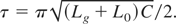
Let us perform a simple analysis on the scheme shown in Figure 1. As shown the experiment, motion of the conductor 4 in Figures 1 and 2 can be presented by variable inductance Lp(t) changing from its initial value L0 to the final value L1. This inductance is almost constant at the inductive storage stage. This allows the energy stored in the capacitor C to be converted into magnetic energy in the inductance Lg + L0. Full energy conversion occurs at the time moment equal to the quarter-period τ of the capacitor discharge in LC circuit:
Consider further rapid change of the inductance Lp and simultaneous connection of the load 2 in Figure 2. For the sake of simplicity, we consider an inductive load with constant inductance Lz = const. The load is connected at the moment when the inductance Lp starts to rise. Neglecting the energy dissipation, the magnetic flux in the circuit at this moment is further conserved, and it is equal to the magnetic flux at the moment when Lp = L1 and when the load current is equal to Iz. This provides us with the following current transfer coefficient:

Here I0 is the generator current at Lp = L0, Iz is the load current at Lp = L1. The energy efficiency coefficient is therefore defined as
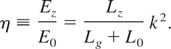
Here E0 is the initial stored energy and Ez is the magnetic energy in the load inductance. For Lz = Lg, L0 → 0 and L1 → ∞ we have η = 0.25 (25 % efficiency) and k = 0.5 (half of the stored current is transferred into the load).
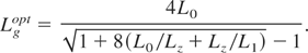
The further logic is the following. The circuit parameters defining feasibility of a pulse power system using the configuration of Figure 1 are L1 (defining the efficiency of inductive switching), the capacitor bank erecting voltage V, and the duration of the inductive storage phase τ, Eq. (2). To optimize the system, let us consider the function η(Lg). Its maximum occurs at
The other important characteristic is the Vτ product, which should be preferably minimized (smaller charging voltages reduce the risk of electric breakdowns and smaller generator current rise-times result in smaller subsequent load current rise-times):
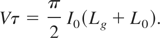
Therefore, for a fixed load inductance and for fixed inductive switch inductances L0 and L1, Eqs. (5) and (6) define the maximum energy transfer efficiency η(Lgopt) and the parameter Vτ.
5. EXAMPLE OF A MEGA-AMPERE GENERATOR
Consider parameters of a pulse power system with inductive load. For example, one could estimate Lz = 5–7 nH as the mean load inductance of a fast z-pinch (Davis et al., 1996; Matzen, 1997). Figure 4 shows calculated values of η(Lgopt) and Vτ(Lgopt) for the load with Lz = 7 nH, Iz = 60 MA and for different values of ΔL = L2 − L1.

Efficiency η and the parameter Vτ (in MV × μs) for L0 = 2 nH (triangles), L0 = 4 nH (squares) and L0 = 6 nH (circles). The load inductance is Lz = 7 nH.
One can see that the increase of L0 considerably decreases the maximum efficiency η and increases Vτ. For example, the value L0 = 4 nH (corresponds to the inductance of electrical connections with the initial conductor position 4 in Fig. 1) yields to η > 10% for ΔL > 30 nH. From the results of Figure 4 and for the case of L1 = 40 nH, one could derive generator characteristics shown in Table 1.
Generator parameters calculated from Figure 4 for the scheme shown in Figure 1

For a microsecond capacitor bank discharge, the primary generator voltage can be maintained at the level of 2–3 MV, i.e., at the values acceptable for existing technologies of microsecond capacitor banks.
The scheme of Figure 1 allows parallel connection of inductive volumes as schematically shown in Figure 5. This relaxes the requirement on the output voltage of the primary generator. For example, at unchanged performance of the scheme (i.e., same Iz,τ,L0, and L1), each capacitor bank is characterized by the parameters shown in Table 2.

Parallel connection to a common load. 1—to two capacitor bank, 2—load, 3—convolute, 4—accelerated conductor, 5—closing switches (dielectric flashover), 6—mechanical support.
Generator parameters calculated from Figure 4 for parallel connection of two inductive switches shown in Figure 5

6. ELECTRICAL CIRCUIT MODEL
Modeling of the electrical circuit of Figure 1 was performed for a z-pinch-type load. Equivalent circuit corresponding to the scheme of Figure 1 can be represented by the following set of equations:
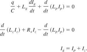
Here C and Lg are the parameters of the capacitive primary storage taken from Table 1. Ig is the generator current; Lp and Ip correspond to the varying inductance and current of the conductor; Lz and Iz are the time-dependent inductance and the current of the load shell. Rs is the resistance of an ideal closing switch connecting Lp and Lz parts (Rs = ∞ during the magnetic energy storage time and then Rs = 0).
The load was assumed to be a perfectly conducting cylindrical shell accelerated by the magnetic field of the load current Iz and having the mass mz = 0.1 g, the height hz = 2 cm, and the initial radius rini = 2.2 cm.
The conductor 4 in Figure 1 was assumed to be a perfectly conducting foil accelerated by the current Ip and having the mass M = 0.2 g. The axial acceleration occurs at the distance h = 5 cm in the space between a cathode, Rc = 50 cm, and an anode, Ra = 55 cm. In order to model the motion of a small current-carrying portion of the conductor mass m shown in Figure 1, the whole conductor mass is divided into two parts at the end of axial acceleration. The mass M − m continues its axial motion. The small mass m is considered as a perfectly conducting cylindrical shell with the height varying in time and equal to zM − h, where zM(t) is the current position of the main conductor mass. This mass is further radially accelerated by the current Ip.
All the moving parts (load shell and the conductor) participating to the whole scheme operation is described by simple equations of motion

Here ξi, Mi, and Ii represent accordingly the coordinate, the mass and the current in the described motion, i.e., z, M, and Ip for the main conductor mass; r, m, and Ip for the residual conductor mass compressed radially; r, mz, and Iz for the load shell. Li are the varying inductances in corresponding geometries. We also assume a 10-fold radial compression ratio for the masses m and mz, i.e., their motion is stopped when the masses reach r = Rc/10 and r = rini/10 accordingly.
Figures 6 and 7 show the results of numerical solution of the Eqs. (7) and (8) describing the scheme of Figure 1. In the beginning of the capacitor discharge, the current flows through Lg and through the axially accelerated conductor with the mass M. When the conductor passes the length h, the load is connected (Rs = 0) and the current starts to flow simultaneously through the shell of residual mass m and through the load shell with the mass mz. Both masses are imploded radially towards the axis of the system, Figure 1.

Circuit modeling result for m/M = 0.01. Generator parameters are taken from Table 1. Parameters of the load and of the inductive switch are defined in the text. (a) Currents Ig (dotted), Ip (solid), and Iz (bold); (b) inductance Lp (solid) and the load liner kinetic energy (bold).

The same modeling result as for Figure 6 with m/M = 0.1.
The voltage generated during compression of the mass m allows the power flow into the load. There is an uncertainty in quantifying the residual mass value m. This value could be obtained only from more realistic, multi-dimensional numerical modeling. Figures 6 and 7 show the general trend in influence of this parameter on the scheme efficiency. For example, consider m = 0.01 M and m = 0.1 M. In both cases the load current Iz reaches the maximum value predicted in Section 5 and the generator-to-load energy transfer efficiency is about 10%. However, the higher is the residual mass m, the slower is its compression, the lower is the voltage across the load inductance and the greater is the load current rise-time.
7. CONCLUSION
In conclusion, we described a scheme of pulsed-power conditioning at high currents. In contrast with the resistive opening switches used on inductive energy storage generators, it is suggested to use the voltage of inductive origin obtained through staged acceleration of a solid-state or plasma conductor. Unlike plasma or solid-state resistors, the inductive impedance may increase with the maximum generator current as in the case of fast z-pinch implosions (Matzen, 1997 and the references therein). The conductor must keep low inductance in order to allow efficient energy coupling to a low-impedance primary generator. The conductor must further increase the inductance in order to provide the transfer of magnetic energy to a load. Principle possibility of such a staged acceleration with power multiplication is confirmed experimentally. Further simple analysis based on magnetic flux conservation in the system shows possibility of a 10% generator-to-load energy transfer efficiency for some realistic generator parameters. Possible uncertainties of the scheme operation are identified to be an additional convolute 3, existence of a residual conductor mass m and a closing switch 5, see Figure 1. The latter could represent a controllable low-inductance dielectric flashover switch (e.g., Kokshenev et al., 2004). Post-hole convolutes are also shown to operate successfully with z-pinch-type loads at mega-Ampere current levels (Spielman et al., 1997). Formation of the residual conductor mass, however, is not studied yet, neither experimentally nor in complicated numerical simulations. We studied the influence of this mass on the scheme efficiency in simple circuit modeling coupled with zero-dimensional equations of motion. The ratio of this mass to the total conductor mass is shown to influence drastically the power multiplication achievable in the scheme.
ACKNOWLEDGMENT
The work was performed under the contract CEG N° 00-25-043-00-470-46-51, Centre d'Etudes de Gramat, France.


