


I. INTRODUCTION
Ultra-wideband (UWB) technologies become hotpot research field for researcher since the Federal communications Commission (FCC) authorized the use of frequency band from 3.1 to 10.6 GHz for short-range wireless communication in 2002 [1]. Lower power requirements, high bandwidth, and reduced fading from multipath propagation are some key characteristics of the UWB communication system. UWB system is a promising technology for short-range indoor wireless communications with increased data rates, as well as radar and geo location applications, unrealizable in traditional narrowband systems. As a vital component of UWB communication systems, exhaustive works have been reportedly made for the design of UWB bandpass filters (BPFs) [Reference Hao and Hong2–Reference Sun and Zhu3]. Lots of efforts and challenges are required to improve the UWB BPFs response such as, low insertion loss, high selectivity, and constant group delay throughout the UWB frequency range. Also several approaches have been applied to improve the compactness and to reduce the design and fabrication complexities.
In recent years, various planar UWB BPFs using different methods have been reported [Reference Zhu, Sun and Menzel4–Reference Alburaikan, Aqeeli, Huang and Hu13]. These techniques can be classified as multiple-mode-resonator (MMR) techniques [Reference Zhu, Sun and Menzel4–Reference Zhang and Xiao5], cascading high-/low-pass filters techniques [Reference Tang and Chen6], hybrid microstrip/coplanar-waveguide (CPW) techniques [Reference Wang, Zhu and Menzel7–Reference Thomson and Hong8], optimum short-circuited stubs techniques [Reference Hong and Shaman9], electronic-band-gap (EBG) structures techniques [Reference Wong and Zhu10], and CRLH-TL-based UWB filter [Reference Bu, Ding and Guo11–Reference Alburaikan, Aqeeli, Huang and Hu13]. In [Reference Zhu, Sun and Menzel4], by forming a MMR and introducing quarter-wavelength parallel coupled lines at the input and output ports, a UWB BPF with five transmission poles is achieved covering the entire UWB frequency band with passband insertion loss and return loss better than 0.55 and 10 dB, respectively. However, the overall length is large, about 16.0 mm. In [Reference Zhang and Xiao5], an UWB filter using the novel MMR is designed has the 3 dB bandwidth of 7.3 GHz from 3.4 to 10.7 GHz with passband insertion loss <0.7 dB and upper-stopband rejection level better than 40 dB. However, the designed filter was large in size and complex to fabricate due to the presence of via. By cascading the BPF and bandstop filters, an UWB BPF is presented in [Reference Tang and Chen6]. However, cascading the BPF and bandstop filters increases the overall size of the UWB BPFs. An UWB filter using hybrid microstrip/CPW surface-to-surface coupling structure is reported in [Reference Wang, Zhu and Menzel7] with five transmission poles in passband has the large overall length of 16.9 mm and, the insertion loss and return loss in the passband is better than 1.0 and 13.5 dB, respectively. In [Reference Thomson and Hong8], a compact UWB filter using parallel coupled microstrip/CPW structure was presented with 3 dB fractional bandwidth (FB) of 90% (from 3.5 to 9.3 GHz) at the center frequency of 6.4 GHz with high passband selectivity. The passband insertion loss and return loss obtained in [Reference Thomson and Hong8] was better than 0.8 and 20 dB, respectively; however, not able to fulfill the FCC requirement for the UWB frequency range. In [Reference Hong and Shaman9], an UWB BPF was reported based on a circuit model of optimum short-circuited transmission line using non-redundant unit elements with FB of 100% where the adjacent short-circuited stubs work as frequency-selective elements, however, difficult to implement. An EBG-embedded MMR-based UWB filter with wide upper-stopband and reduced overall length of 12.5 mm is presented in [Reference Wong and Zhu10]. It has the passband bandwidth of 4.0–10.6 GHz and, the insertion loss in passband lower than 0.8 dB and higher than 15 dB in upper-stopband.
The UWB BPF designs based on composite right/left-handed transmission line (CRLH-TL) were proposed in [Reference Bu, Ding and Guo11–Reference Alburaikan, Aqeeli, Huang and Hu13]. The proposed filter in [Reference Bu, Ding and Guo11] was designed by cascading interdigital lines and three units of defected ground structure (DGS) has greater insertion loss (1.5 dB). An UWB filter presented in [Reference Ahmed and Virdee12] based on CRLH-TLs has wide upper-stopband with the rejection level higher than 18 dB and 115% 3-dB FB within 2.9–10.75 GHz. Here the filter was designed using symmetric unit-cell composed of interdigital coupled line with a short-circuited inductive stub to improve selectivity and insertion loss in passband. The designed filter has passband insertion loss <0.5 dB, return loss better than 10.0 dB but large physical length of 16.4 mm. In [Reference Alburaikan, Aqeeli, Huang and Hu13], a novel UWB BPF based on CRLH-TL unit cell was designed by cascading interdigital coupled line with a low-pass filter based on SSRR (symmetrical split-ring resonator) DGS. The filter has the wide upper-stopband with attenuation level >23.0 dB both in lower and upper stopband, an insertion loss of 1.0 dB, return loss better than 13 dB with more than 100% FB. The UWB BPFs presented in [Reference Bu, Ding and Guo11–Reference Alburaikan, Aqeeli, Huang and Hu13] were designed based on the transmission line approach of left-handed (LH) metamaterials, where shunt stubs need to be connected to the ground plane through vias, which increases the fabrication complexity and also lead to expensive backside processing. Some more UWB BPFs [Reference Abbosh14–Reference Xia, Wu and Mao16] are considered in this paper for the comparison purpose with the proposed UWB BPF. In [Reference Abbosh14–Reference Abbosh15], broadside coupled microstrip-slot-microstrip structures are utilized to obtain UWB response. In [Reference Xia, Wu and Mao16], the UWB performance was achieved with a pair of symmetrical UWB filtering units based on differential transmission lines and three DGS units in the ground plane. However, the designed UWB filters in [Reference Abbosh14–Reference Xia, Wu and Mao16] are large in size and complex to implement.
In this paper, a novel and highly compact UWB BPF is proposed based on CRLH-TL composed of capacitive gap in conductor strip and meander fractal like ring slot in ground plane with 142% FB. Wider passband bandwidth can easily be achieved by properly adjusting the overall length (perimeter) of the ring slot and the slot width in the ground plane, and the gap between the conductor strips at the top plane. The meander-shaped ring slot in the ground helps to improve in-band return-/insertion loss and out-of-band performances. The upper-stopband performance is primarily affected by the lengths/widths of stepped-impedance lines and the ring slot in the ground plane. The equivalent circuit model of proposed UWB filter is provided here for better insight into the operation mechanism and electrical parameters are extracted using the circuit model tool of Ansoft designer. The prototype of optimized UWB filter is fabricated and measured for experimental verification. Measured results show that in the entire passband (3.14–18.26 GHz) the proposed UWB filter achieves insertion loss <0.5-dB, return loss better than 10-dB with five transmission poles. The sharp and deep out-of-passband rejection skirts with rejection level more than 30 and 20-dB at the lower and upper-stopband, respectively, is achieved.
II. DESIGN OF PROPOSED UWB BPF AND EQUIVALENT CIRCUIT MODEL
The layout of the proposed UWB BPF is shown in Fig. 1(a). The proposed filter is designed using three sections of stepped-impedance transmission lines (shown in black) on both side of symmetrical design and a CRLH-TL synthesized with series capacitive gap in conductor strip and meander fractal like ring slot (shown in white) in the ground plane (shown in gray). The topologies of top and bottom with all dimensional parameters are shown in Figs 1(b) and 1(c), respectively. It has been demonstrated that, in microstrip technology a one-dimensional LH metamaterial may be designed by etching complementary split-ring-resonators (CSRRs) in the ground and a capacitive gap in conductor strip. Since right-handed (RH) effect is intrinsic in the actual design, this LH metamaterial transmission line is termed as composite CRLH-TL in the manuscript. As shown in Fig. 1(b), the top plane of proposed filter consists of two stepped-impedance lines of dimensional parameters L 2, L 3, W 2, and W 3. The third section is a 50 Ω transmission line with parameters L 1 and W 1 for input/output ports. The ground plane is basically a rectangle of size 10 × 8.6 mm2 with loaded meander fractal like ring slot of slot width a. The parameters b and c are the width of metallic part inside ring slot and width of outer boundary of ground plane outside ring slot. The meander fractal like ring slot in the ground plane and conductor strips with gap at the top plane play their own role to get the UWB bandpass response. The gap in conductor strip or etching slot in ground alone is not able to obtain wide bandwidth. Wider bandwidth is achieved when both, gap and ring slot in ground plane exist simultaneously. When meander like ring slot is etched at the ground and there is no gap between the conductor strips at top, low insertion loss is obtained, whereas when meander like ring slot is not etched at the ground and the gap is present at the top, a very high insertion loss is obtained and electromagnetic (EM) wave is cut-off up at the bandwidth of interest. However, when both meander fractal like ring slot in the ground plane and gap between the conductor strips are present simultaneously, a very broad bandpass response can be obtained. Negative permeability is realized when gap is used in conductor strip and meander fractal like ring slot is used to realize negative permittivity [Reference Falcone, Lopetegi, Baena, Marques, Martín and Sorolla17–Reference Lai, Itoh and Caloz19]. Now, the length and width of high/low stepped-impedance transmission lines are adjusted to improve passband return loss and out-of-band performance. Simultaneously, the gap between conductor strips, and the size (perimeter) and width of ring slot in the ground is also optimized to adjust the passband lower and upper cut-off frequencies. Also the length and width of conductor strip are optimized to reduce the insertion loss in the desired frequency band of interest and to improve out-of-band rejection capability. The proposed UWB BPF is designed on RT/Duroid 5880 substrate with dielectric constant of 2.2, thickness of 0.508 mm, and is optimized using commercial full wave EM simulator IE3D.

Fig. 1. Topology and equivalent circuit of proposed UWB filter: (a) proposed UWB bandpass filter, (b) top view, (c) bottom view, and (d) equivalent circuit model.
The lumped equivalent circuit model gives the deep insight to understand the behavior of the proposed geometry. The lumped equivalent circuit model of the proposed geometry is illustrated in Fig. 1(d). The lumped parameters of circuit model and results are obtained using circuit model tool of Ansoft Designer. In the lumped equivalent circuit diagram, the mutual coupling between the individual elements is not taken into consideration. The input and output inductive components each of value L is introduced because of the input and output conductor strips. The capacitance C L is generated due to the gap of width (d) between the conductor strips. The coupling capacitor C c is included because of the coupling between the top plane conductor strips and the part of meander ring slot in the ground plane. The meander ring slot resonator is modeled by tandem tank circuit consists of series C F and L L and parallel R, where R accounting for the losses. The input and output 50 Ω microstrip transmission lines each of length 14.2 mm are used to compensate the phase response and to represent parasitic RH effect in the proposed geometry. The extracted parameters of the equivalent circuit model are as follows: L = 0.5 nH, C L = 0.4 pF, C c = 1.12 pF, C F = 0.1 pF, LL = 0.45 nH, and R = 1.76 kΩ.
The comparative simulated and circuit model S-parameters versus frequency plot of the proposed geometry is depicted in Fig. 2. It is observed that the circuit model results are in good resemblance with the simulation results, except the response at some higher frequency near upper-stopband. The simulated insertion loss |S 21| is ≤ 0.5 dB in the frequency band from 2.95 to 18.38 GHz with |S 11| > 10 dB, whereas the equivalent lumped circuit model insertion loss |S 21| is ≤ 0.5 dB throughout the frequency band from 3.0 to 18.14 GHz. The discrepancy between these results may be due to well-known fact that in very wide bandwidth, the proposed structure operates at different manners and the circuit models are not always accurate in very wide bandwidth, but still the circuit model provides the main operation principle. The main factor of getting an UWB response is the presence of meander ring slot in the ground plane, which offers the series C F and L L in the tandem tank circuit. Increasing the values of C F and L L decreases the higher cut-off frequency of the filter. While extracting the parameters of lumped circuit model, following points have been noted: (1) Increasing the inductance value L offered by conductor strips from 0.5 to 0.8 nH, the passband S-parameters performance becomes poor (|S 21| < 1.31 dB and |S 11| < 6.5 dB). (2) The effects of changing the capacitor, C L generated by coupling gap between the conductor strips can be seen in the lower cut-off frequency of the UWB BPF. For |S 21| ≤ 0.5 dB, by increasing the value of C L from 0.1 to 2.0 pF, the lower cut-off frequency of the proposed UWB BPF changes from 4.38 to 1.45 GHz. (3) The overall bandwidth of the filter can be controlled by the coupling capacitor C c , and components C F and L L of tandem tank circuit.

Fig. 2. Comparative simulated and equivalent lumped circuit model S-parameters versus frequency plot.
III. PARAMETRIC STUDY AND MEASURED RESULTS
To obtain the better in-band and out-of-band performance, the dimensional parameters of proposed UWB filter are optimized. Optimization of dimensional parameters is performed by varying one parameter at a time while keeping the other parameters unchanged. The simulated S-parameters versus frequency plot with capacitive gap in conductor strip “d” is depicted in Fig. 3. It is found that the lower cut-off frequency is shifted toward higher-frequency edge with increased value of “d” while maintaining the passband and upper-stopband performances. So the parameter “d” is primarily responsible to control the lower cut-off frequency. Better passband and out-of-band stopband performance is observed for d = 0.2 mm. The variations in insertion loss and return loss with fractal like ring slot width “a” is represented in Fig. 4. It is observed that, the higher cut-off frequency is increased with increasing slot width, while the passband insertion loss and return loss are also increased. The choice a = 0.2 mm provides the better passband and stopband performance. It has been experimentally observed that the first resonance frequency of passband can be lowered by increasing the length (perimeter) of the ring slot in the ground plane.

Fig. 3. Simulated S-parameters performance with parameter d.

Fig. 4. Effect of slot width parameter “a” in the ground plane.
Variation in S-parameters with length (perimeter) of ring slot is represented in Fig. 5 with 10% decrease and increase in the overall length of meander fractal like ring slot compared with the proposed length. It is observed that both the lower and upper cut-off frequencies are shifted toward the lower edge frequency with increased length of the ring slot. So, both lower and upper cut-off frequencies can be controlled by properly adjusting the length of ring slot. It can be seen that better in-band and out-of-band performance is obtained with proposed length of ring slot. Also the peaks of passband insertion loss and return loss get enhanced when the length of the slotted section is changed compared with the proposed one. Spurious band in the stopband is observed when length of ring slot is increased compared with the proposed length.

Fig. 5. Effect of size (perimeter) of ring slot in the ground plane.
The variations in insertion loss and return loss with parameter “W 2” and “W 3 are depicted in Fig. 6(a) and (b), respectively. As observed from Fig. 6(a), return loss in the lower passband frequency edge (at 5.2 GHz) is improved with increasing value of “W 2”, while in the middle of passband (at 12.6 GHz) return loss is increased. The insertion loss in the entire passband is almost unchanged. Minor shift in the upper cut-off frequency toward higher-frequency edge is also observed with increasing “W 2”. Better in-band and out-of-band performance is observed for W 2 = 5.1 mm. As shown in Fig. 6(b), the higher value of W3 increases the return loss in the middle of the passband at about 8.1 and 12.5 GHz, while decreases at lower-frequency edge at 4.8 GHz; however, the upper cut-off frequency in passband is reduced with “W 3”. Therefore the overall passband frequency bandwidth is also reduced. Adverse effect is seen for lower value of “W 3”. In the upper-stopband, the insertion loss gets sharpened at the lower edge with increased value of “W 3”; however spurious bands are also increased. Better performance is observed for W 3 = 6.4 mm.

Fig. 6. Simulated S-parameters with variations in parameter: (a) W 2 and (b) W 3.
The parameters “L 2” and “L 3” of stepped-impedance lines are adjusted to improve the in-band and out-of-band performance while maintaining the overall size of proposed UWB filter. The parameters L 1, L 2, and L 3 are interrelated to each other, i.e. variation in any one parameter will change the dimension of another parameter. The variation in S-parameters for different values of parameters “L 2” and “L 3” are plotted in Figs 7(a) and 7(b). It is observed that the higher the values of “L 2” and “L 3”, the lower the return loss in the passband, while the insertion loss is increased for lower values of “L 2” and “L 3” at the higher-frequency edge in the passband. Optimized dimensions of “L 2” and “L 3” are found as L 2 = 0.75 mm and L 3 = 1.4 mm. The first section of stepped-impedance line is a 50 Ω transmission line used as input/output ports where, the dimension of parameter “W 1” is chosen according to 50 Ω transmission line. The optimized dimension of different parameters of proposed UWB BPF is summarized in Table 1. For optimized parameters, the simulated insertion loss is ≤0.5 dB in the frequency band from 2.95 to 18.38 GHz with |S 11| > 10 dB. The sharp and deep out-of-passband rejection skirts with rejection level more than 30 and 20 dB at the lower and upper-stopband respectively is achieved.

Fig. 7. Simulated S-parameters with variations in parameter: (a) L 2 and (b) L 3.
Table 1. Optimized values of dimension parameters for proposed UWB filter.

A prototype of proposed UWB BPF shown in Fig. 1(a) is fabricated and measured to evaluate the performance, and to validate the simulation results. The fabricated photograph of the top and bottom of proposed UWB filer are represented in Fig. 8(a) and (b), respectively. The comparison between simulated, circuit simulation and measured S-parameters is shown in Fig. 9. Very reasonable agreement is found between the simulated and measured S-parameters within the entire passband and stopband, thereby the actual realization of proposed UWB filter is confirmed. The measured 10 dB return loss bandwidth is found from 3.14 to 18.26 GHz with FB of 142%. The insertion loss is almost close to 0 dB; however is <0.5 dB in the entire passband. Compare with six transmission poles in the simulation, five transmission poles are found in measurement results. The slightly large insertion loss in measured result at higher-frequency edge in passband is mainly attributed due to low dielectric constant of the substrate used. In the upper-stopband, the measured insetion loss is higher than 13 dB from 19.7 to 24.4 GHz with return loss better than 1.5 dB, while simulated insertion loss is better than 15 dB from 20.2 to 24.5 GHz. Also, deep and sharp rejection skirts at both lower and upper stopband are observed. In the lower-stopband, the rejection level is better than 30 dB for both simulation and measurement. However, in the upper-stopband, the rejection level in measurement is better than 30 dB compare with 20 dB in simulation. The little discrepancy between simulated and measured results seen may be due to imperfect soldering of SubMiniature version A (SMA) connector and manufacturing tolerances.

Fig. 8. Photograph of fabricated prototype: (a) Top view (b) Bottom view.

Fig. 9. Simulated, circuit model and measured S-parameters of proposed UWB bandpass filter.
Fig. 10 shows the comparative phase responses obtained from simulation, measurement and the circuit model of proposed UWB filter. Good agreement is observed throughout the entire frequency band of interest except at lower and higher frequencies in the stopband regions. It is observed that the results obtained are consistent with each other except at lower and higher frequency bands for the circuit model. The slight and permissible phase shifts between these results may be seen, because in very wide bandwidth, the proposed structure operates in different manners and the circuit model may not be always accurate in very wide bandwidth. The simulated and measured group delays of proposed UWB BPF are shown in Fig. 11, and found to be consistent with each other. It is observed that the measured group delay varies between 0.85 and 1.5 ns. Thus, the maximum variation of 0.65 ns is obtained within the desired frequency bandwidth of interest from 3.14 to 18.26 GHz, showing a good linearity. The performance parameters, filter's size and structure's complexity are compared with other best reported UWB BPFs in Table 2.

Fig. 10. Phase response of proposed UWB bandpass filter.
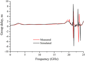
Fig. 11. Group delay performance of proposed UWB bandpass filter.
Table 2. Comparison with other UWB bandpass filters.

IV. CONCLUSION
A novel and highly compact UWB BPF using stepped-impedance transmission lines and a CRLH-TL synthesized with meander fractal like ring slot in ground and series capacitive gap in conductor strip is designed, fabricated and measured. The response of the proposed UWB filter is optimized using parametric study, and further verified by circuit simulation and measurement. The proposed UWB BPF is highly compact in size with overall dimension of 10 × 8.6 mm2. From the measurement, very wide passband bandwidth from 3.14 to 18.26 GHz with return loss better than 10 dB and insertion loss <0.5 dB is found. Also, the proposed filter possesses wide upper-stopband of 19.7–24.4 GHz with insertion loss higher than 13 dB and return loss better than 1.5 dB. Compactness, good phase linearity, small fluctuation in group delay, and good passband and stopband performance make the proposed filter a suitable candidate for UWB applications.
 Babu Lal Shahu has been working as an Assistant Professor in the Department of ECE, Birla Institute of Technology, Mesra, Ranchi, Deoghar Campus since May, 2009. He received his Bachelor degree (B.E.) in Electronics Engineering in year 2003 from RGPV Bhopal and post-graduated (M.E.) in Wireless Communication from the Department of Electronics and Communication Engineering, Birla Institute of Technology, Mesra, Ranchi, in 2007. His present research interests include Fractal geometries-based microwave circuits for wireless communications, RF circuits design, and Defected ground plane.
 Srikanta Pal has been working as a Professor in the Department of ECE, Birla Institute of Technology, Mesra, Ranchi, since 2011. He graduated in Electronics and Communication Engineering in 1990 at NIT Warangal and post-graduated in Microwave Engineering from Jadavpur University, Kolkata, in 1992. He was awarded D.Phil. from the University of Oxford, United Kingdom, in 2003 for his research into High Temperature Superconducting microwave filters. During 1992–2000, he worked in Bharat Electronics Limited (BEL) in the Departments of R & D as a Senior Engineer. In 2006, he started Post-doctoral Fellowship at the University of Birmingham under Professor Mihael J. Lancaster, where he worked on Superconducting filters for radio astronomy and RF MEMS. His present personal research interests include Microwave, Millimeter wave circuits and components, RF MEMS, as well as the High-frequency properties and applications of novel and diverse materials.
 Neela Chattoraj is presently working as an Associate Professor (Electronics & Communication Engineering) at Birla Institute of Technology (BIT), Mesra, Ranchi. She received her B.E. from BIT Mesra and completed Ph.D. in 2007. She worked in CSIR during 1988–1992 and as Project Engineer under MHRD till 2001. She completed the project on MEMS in the year 2014. Her area of research interest includes Antenna design, Genetic algorithm, Microwave circuits, and MEMS. She has published many papers on MEMS phase shifter, MEMS switch, Reconfigurable antennas, Genetic algorithm, Fractal antennas, UWB antennas, and Dual-band and multi-frequency antennas.
 Dileep Kumar Upadhyay is presently working as an Assistant Professor in the Department of ECE, Birla Institute of Technology, Mesra, Ranchi since August 2007. He has received his graduate degree (B.Tech.) in Electronics and Communication Engineering in year 2005 from Uttar Pradesh Technical University (UPTU) Lucknow and post-graduated (M.E.) degree in Wireless Communication from the Department of Electronics and Communication Engineering, Birla Institute of Technology, Mesra, Ranchi, in 2007. He has received his Ph.D. (Eng.) degree in March, 2014 on the topic of “Characterization and Experimental Verification of new Microwave Circuits, using Metamaterials in Wireless Communications”, from the Department of Electronics and Communication Engineering, Birla Institute of Technology, Mesra, Ranchi. His present research interests include RF circuits design, Design and development of metamaterial-based microwave circuits, Defected ground plane and fractal geometries-based microwave circuits for the applications in wireless communication systems.


