I. INTRODUCTION
A rapid growth in wireless technology attracted huge attention from the industry and research community to make self-sustainable devices feasible through radiofrequency (RF) energy harvesting. It truly alleviates the frequent battery replacement problem or even it can reduce the battery requirement altogether. According to the Friss transmission equation, the received signal strength reduces with the square of distance (d) between the transmitter and the receiver. Thus, it has become a challenge to increase the rectenna output voltage by harvesting as much energy as possible in such low-power density environment. Since in ambient the available RF energy not only presents in the single-frequency bands, it mostly spread over the broad range of frequency from 820 MHz to 2.5 GHz (cellular bands and Wi-Fi) [Reference Rabah, Seetharamdoo, Addaci and Berbineau1]; therefore, multi or broadband rectenna can be served a promising approach to improve the RF-to-dc conversion efficiency. For this to be feasible, rectenna system needs to have a multi/broadband antenna and a multi or broadband matching network. As mentioned previously, RF signal strength continuously degraded with distance and can be from any direction; therefore, the broadband antenna having high radiation efficiency, stable pattern and optimum gain is needed to develop an efficient rectenna system.
In the literature, various high-efficiency antennas with circular polarization have been reported for narrow bandwidth [Reference Chen, Yang, Zhao and Fu2, Reference Chen, Guo, Qin and Fu3]. For instance, in [Reference Chen, Yang, Zhao and Fu2] a circularly polarized microstrip antenna achieves the efficiency >97% over a limited frequency band of 0.96 to 1.2 GHz. In [Reference Chen, Guo, Qin and Fu3] also, three-dimensional (3D) printed circularly polarized antenna is reported with efficiency more than 95%, but the bandwidth was only 20.8% (1–1.3 GHz). In contrast, for RF energy harvesting a broadband antenna from 0.84 to 2.4 GHz is required. Previously, several planar ultra wideband antennas with optimum gain value have reported in [Reference Zhou, Li, Wang, Feng and Liu4, Reference Ellis, Zhao, Wu, Nie and Liu5, Reference Dikmen, Cimen and Cakir6]; however, the radiation pattern was not uniform through the entire bandwidth. Besides, some broadband antennas with a stable radiation pattern are reported in [Reference Rabah, Seetharamdoo, Addaci and Berbineau1, Reference Arrawatia, Baghini and Kumar7]. In [Reference Rabah, Seetharamdoo, Addaci and Berbineau1], a wideband antenna achieved the total impedance bandwidth from 0.67 to 12 GHz with a stable radiation pattern, but the efficiency was lie between 25 and 87%. In [Reference Arrawatia, Baghini and Kumar7], a triangular-shaped monopole antenna exhibits a stable radiation pattern over the band from 0.85 to 1.94 GHz although the radiation efficiency and the gain was only 75% and 2 dBi, respectively, thus not so advantageous for energy-harvesting application.
To address this, a broadband antenna with high efficiency, uniform pattern, and optimum gain value is required for RF energy harvesting. As compared with conventional metallic antennas dielectric resonator antenna (DRA) exhibits several unique characteristics such as low dissipation loss, low profile, and more design flexibility, which make it perfect candidate for high-efficiency broadband wireless applications. In this work, a broadband hybrid DRA is proposed. The proposed DRA not only promises the broad impedance bandwidth of 110% (0.86 to 3 GHz), but also exhibits high radiation efficiency (above 90%) and peak gain of 6.8 dBi with a uniform radiation pattern across the entire bandwidth. In addition, a dual-band rectenna where the proposed antenna is matched with the rectifier at two public telecommunication bands of GSM-900 and GSM-1800 using a compact hybrid dual-band matching network, is proposed. The measured result demonstrates that the proposed dual-band rectenna system provides the peak efficiency of 65 and 59% for a load impedance of 4.7 kΩ for a load impedance of 4.7 kΩ at 0.9 and 1.8 GHz, respectively. This paper is organized as follows. Section II shows the state-of-the-art. Section III presents the antenna geometry and its parametric study. Section IV, discusses the measured results of the antenna, whereas Section V focuses on realization of dual-band rectenna system and its measured results. Section VI concludes this work.
II. STATE-OF-THE-ART: BROAD BAND DRA
From the past two decades, DRA attracted huge attention owing to attractive features such as small size, high radiation efficiency, and light weight. Previously, several techniques have been reported to broaden the DRA bandwidth. One of these methods usesstacked or multiple layers of different size and dielectric constants to increase the bandwidth of the DRA [Reference Huang and Kishk8]. Other approach is to use the special feeding mechanisms were proposed for bandwidth enhancement [Reference Zhang, Zhong and Xu9, Reference Gao, Feng and Zhang10]. For instance, Zhang et al. [Reference Zhang, Zhong and Xu9] and Gao et al. [Reference Gao, Feng and Zhang10] have proposed an elliptical microstrip patch and inverted trapezoidal conformal line to feed the U- and T-shaped DRA, respectively, and achieved the bandwidth above 70%. Different geometries such as U-shape [Reference Zhang, Zhong and Xu9], T-shape [Reference Gao, Feng and Zhang10], E-shape [Reference Gupta and Parihar11] , and L-shape [Reference Liang, Denidni and Zhang12] were also proposed to broaden the DRA bandwidth. However, the above techniques [Reference Huang and Kishk8, Reference Zhang, Zhong and Xu9, Reference Gao, Feng and Zhang10, Reference Gupta and Parihar11, Reference Liang, Denidni and Zhang12] increase the complexity and volume of the DRA and require someadditional processes to modify the DRA geometry, which may increase the implementation cost of the DRA. The difficulties due to complex structure can be illustrated in [Reference Gao, Feng and Zhang10, Reference Liang, Denidni and Zhang12], where two different volumes of DRAs were stacked to form a T and L-shaped DRA, respectively. Moreover, the impedance bandwidth for both structures were reported below 76%.
Thus, in order to enhance the bandwidth and to reduce the structure complexity of DRA, another method where DRA is integrated with the microstrip patches, slot, or any other kind of radiator often known as hybrid DRA, is used. The advantage of this methodis that it offers the size miniaturization and preserves the antenna polarization and radiation pattern within the working frequency band [Reference Buerkle, Sarabandi and Mosallaei13–Reference Esselle and Bird15], which is very essential for an efficient energy harvesting prospective. In this paper, a simple low-profile broadband hybrid DRA is proposed, where a pentagon shape DRA is loaded by a rectangular slot situated in the ground plane. The detailed antenna structure is presented in the next section.
III. ANTENNA ARCHITECTURE AND PARAMETRIC STUDY
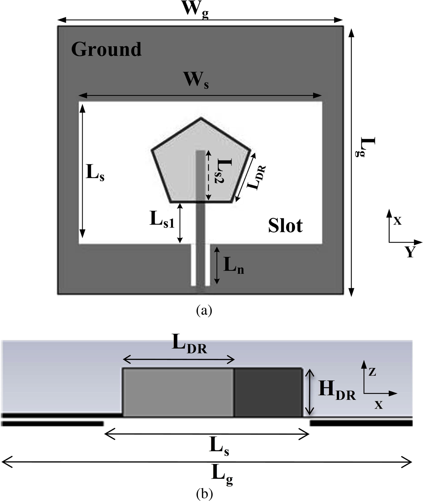
Figures 1(a) and 1(b) show the cross-sectional and bottom views of the proposed antenna. The antenna is fabricated on FR-4 with a thickness of 1.5 mm. The DR is made of Rogers RO3010 of dielectric constant (ε DR) 10.2. The DR shape is pentagon with height of h DR and arm length L DR. As depicted in Fig. 1, DR is fed by the underlying rectangular slot of size (L s × W s) with a small notch of depth L n, which ensure strategic perturbation in the current distribution and results in good impedance matching over the wide frequency range. With reference to Fig. 1, there are various parameters, which may influence the antenna performance. For more insight, an extensive parametric study is carried out using a full-wave electromagnetic simulator CST Microwave Studio [Reference Jung, Choi and Choi16].

Fig. 1. Geometry of the PDRA: (a) the top view and (b) the side view.
A) Feed line length (L s2)
The effect of feed line length (L s2) on antenna reflection coefficient is shown in Fig. 2(a). The feed line controls the coupling between the DR and the slot, resulting in variation in impedance matching. The simulations result show that smaller value of L s2 results in mismatched resonances. For instant, the L s2 = 0 curve demonstrates three resonances but with poor impedance matching. However, the value of L s2 = 10 mm leads to the improved impedance matching at each resonance.

Fig. 2. Simulated |S 11| for different values of (a) feedline length (L s2) and (b) slot width (W s).
B) Slot width (W s)
Slot width has an important role in the hybrid antenna design. It affects the coupling of electromagnetic energy from the feed line to the DR and excite the different resonant mode of the DR. Thus, in order to have maximum coupling and to combine the multi-resonant mode of the hybrid structure slot width is optimized. The variation of the proposed antenna reflection coefficient with different slot length is shown in Fig. 2(b). It is noted that by increasing the slot length leads to wider impedance bandwidth which saturated around 107.2% for W s = 88 mm. It is clearly seen that for W s = 52 mm, the proposed antenna achieved the impedance bandwidth of 25%, whereas for W s = 88 mm, it becomes larger by 65.7%, i.e. 107.2%.
C) Notch depth (L n)
A small rectangular notch right below the feed line has a large impact on total impedance bandwidth. It acts as a matching element because it helps to produce pure resistance by nullifying the inductive nature of the antenna [17]. To show its importance, first it is removed from the ground plane by assuming the parameter L n equals to 0 mm in Fig. 1 while keeping all other antenna dimensions constant. The effect of notch length on the reflection coefficient of the proposed hybrid antenna is illustrated in Fig. 3. It can be seen that the notch length (L n) has significant effect on reflection coefficient of the antenna. This creates a strategic perturbation in the current distribution, which leads to improved impedance bandwidth. As shown in Fig. 3, the proposed antenna achieved the best matching at L n = 20 mm.

Fig. 3. Simulated |S 11| for different values of notch depth (L n).
After parametric study, the optimized parameters value of the proposed antenna are as follows: W g = 120, L g = 100, W s = 88, L s = 42, L n = 20, L DR = 14, H DR = 6, L s1 = 13, and L s2 = 10 (all in mm).
IV. ANTENNA MEASUREMENT RESULTS
Based on the optimized values found through the parametric study, a prototype is fabricated and tested to validate the theoretical results. Figure 4 demonstrates the photographs of the fabricated antennas with and without DR. Figure 5(a) shows the simulated and measured |S 11| of the proposed antenna. The measured results show reasonable agreement with the simulated one. The slight difference between the simulation and measurement can be accounted for fabrication imperfections. As illustrated in Fig. 5(a), when the structure is without DR it covers the band from 2.6 to 3.4 GHz. On the other hand, when the structure is with DR the lower frequency shifts to 0.86 GHz and the higher shifts to 3 GHz and shows a improved impedance matching. In this case, the measured bandwidth for |S 11| ≤ −10 dB covers a frequency range from 0.86 to 3 GHz, which is about 110.8% with reference to the center frequency of 1.93 GHz; whereas the simulated impedance bandwidth is about 107.2%, covering a frequency range from 0.81 to 2.7 GHz.

Fig. 4. Photographs of the fabricated prototype: (a) without DR and (b) with DR.

Fig. 5. (a) Simulated and measured |S 11| with and without DR and (b) simulated and measured gain and simulated efficiency.
In the proposed antenna, the pentagon DRA is fabricated manually by stacking of multiple substrates of high dielectric constant (10.2) and it was mounted on the printed slot etched (through conventional lithography technique) on another substrate of low dielectric constant (4.3); hence, there may be the possibility of small air gaps left between different DR layers and some spacing may be also exist between slotted substrate and pentagon DRA during the placement of DRA over the slot antenna. This air gap will reduce the effective dielectric constant, which may result in enhanced bandwidth. Moreover, a small misalignment between DRA and slot may also affect the measured bandwidth.
Figure 5(b) shows the simulated and measured peak gain of the antenna. It can be seen that the measured gain is higher than the simulated gain throughout the frequency band and has the maximum value of 6.8 dBi at 2.5 GHz. Due to unavailability of anechoic chamber the gain measurement was performed in the laboratory environment, where it may receive multiple reflections from the different directions, which may be constructive in nature and result in increased antenna gains. Besides, the small air gaps left between different DR layers and some spacing left between the substrate and pentagon DRA during the placement of DRA over the slot antenna may also increase the measured gain due to reduction in the effective dielectric constant. From the inset graph of Fig. 5, it is noticed that antenna's radiation efficiency is above the 90% within the frequency band of 0.9–2.7 GHz. It was calculated from the simulated gain and directivity definitions, neglecting losses due to impedance and polarization mismatch.
Figure 6, shows the simulated (hollow) and measured (solid) radiation patterns in the yz- (black pattern) and xz-planes (red pattern), respectively. Three most useful frequencies 0.9, 1.8 and 2.4 GHz suitable for RF energy harvesting were chosen for comparison. It is noticeable that in the xz-plane the measured patterns are bidirectional and show close agreement with the simulated results at all frequencies. Moreover, it is confirmed through simulation that the proposed antenna is linearly polarized in the entire frequency band.

Fig. 6. Simulated and measured radiation patterns of the antenna.
The surface current distribution at four different frequencies of the antenna is illustrated in Fig. 7. It can be seen that at 0.88 GHz, the surface current is mostly concentrated on the edges of the wide rectangular slot which is continually decreasing as the frequency of operation is increased to 2.5 GHz. At this frequency, the current is mostly distributed around the edges of small notch just below the feed line. These two slots when combined with DRA give a wide band operation from 0.88 to 3 GHz. Here three different resonance modes, i.e. modes of wider slot, notch, and DRA are merged together to obtain a wide band operation.

Fig. 7. Surface current distribution of the proposed antenna at (a) 0.88, (b) 1.42, (c) 2.1, and (d) 2.5 GHz.
V. DUAL-BAND RECTENNA
A dual-band rectenna is designed and tested using the developed broadband DRA. The rectenna consists of proposed antenna, a dual-band impedance matching and a single-series circuit with one double diode on a lossy FR-4 substrate. In this paper, Schottky diode HSMS-285C with spice parameters (V th = 150 mV, C j = 0.18 pF, and R s = 25 V) is used to convert RF signal into DC voltage due to low threshold voltage and high switching speed. Since, diode is a non-linear device, therefore harvesting circuit itself exhibits non-linearity i.e. its input impedance varies with the received RF power, which makes difficult to retain the impedance match over a wide-frequency range. Therefore, it is preferable to harvest energy from several narrow frequency bands rather than a single large one. The idea underlying the adopted dual-band matching network is 1-n frequency. The detailed analysis of the dual-band rectifier circuit is discussed in the next subsection.
A) Dual-band rectifier
Figure 8(a) shows the equivalent circuit diagram of the dual-band rectifier circuit. As seen, the impedance matching at two frequencies is achieved by means of a combination of two series and parallel LC pairs (L 1 C 1 and L 2 C 2) whose values were calculated through the 1-n frequency transformation method. In order to avoid any impedance mismatch due to small difference in elements value, the meander line inductor and open stub are used to realize the inductors and capacitors, respectively. In this case, not only fabrication and optimization processes become easy but cost will also reduced. Further, it has been demonstrated in [Reference Nintanavongsa, Muncuk, Lewis and Chowdhury18, Reference Agrawal, Pandey, Singh and Parihar19] that the number of rectifying diodes or equivalently voltage multiplier stages are very much sensitive to the RF-to-dc efficiency. In the low-power region (≤−20 dBm) efficiency decreases if voltage multiplier stages are increased, while in the high-power region (≥−20 dBm) an opposite effect is occurred. As the demand is to harvest energy in the low-power region, therefore a single-series circuit with a double diode is used in the proposed circuit. The layout of the dual-band rectifier is shown in Fig. 8(b).

Fig. 8. (a) Equivalent circuit diagram of dual-band rectifier circuit and (b) layout of the dual-band rectifier circuit.
The photograph of the dual-band rectifier circuit is shown in the inset of Fig. 9(a). It is fabricated on a 1.54-mm-thick FR-4 substrate with a dielectric constant (ε r) of 4.3 using a chemical etching method. The rectifier performanceis evaluated in terms of |S 11| and output voltage using the Agilent vector network analyzer (VNA). The simulated and measured |S 11| of the rectifier circuit is shown in Fig. 9(a). The measured result shows reasonable agreement with the simulated one; slight difference can be accounted for the fabrication imperfections. It is well known that the impedance matching is a function of frequency and input power due to non-linearity of the diode. Such characteristic is examined in Fig. 9(b), where the |S 11| is demonstrated as a function of frequency for different power levels from −20 to 10 dBm. It is shown that the proposed rectifier circuit is reasonably matched at the selected frequency bands for a broad range of input power.

Fig. 9. (a) Simulated and measured |S 11| of the rectifier and (b) measured |S 11| of the rectifier at different input power.
B) Rectenna's results and measurement
In this section, the dual-band rectifier circuit is connected to the broad band pentagon-shaped dielectric resonator antenna (PDRA) in order to realize the dual-band rectenna system. The setup shown in Fig. 10, is used to evaluate its performance. For testing, two antennas were used: one for the transmission of RF power and second one for the RF reception. Initially, Agilent's VNA is placed at point a, which is used here as a signal generator of different frequencies. The received power is measured at the far-field distance at point b by connecting the proposed antenna to the Agilent's spectrum analyzer. Subsequently, the spectrum analyzer was removed and rectenna (antenna + rectifier) is placed at the same location and then dc voltage is measured across the load R. Same measurement steps are repeated for the other frequency. The rectifier and rectenna output measured across the load value of 4.7 kΩ is depicted in Fig. 11(a). It can be seen that the rectenna system achieved a maximum output voltage of 4.4 V at 10 dBm input power. Figure 11(b) shows the measured RF-to-dc conversion efficiency of the rectifier and the rectenna system measured across the same load resistance of 4.7 kΩ.

Fig. 10. Rectenna performance measurement setup.
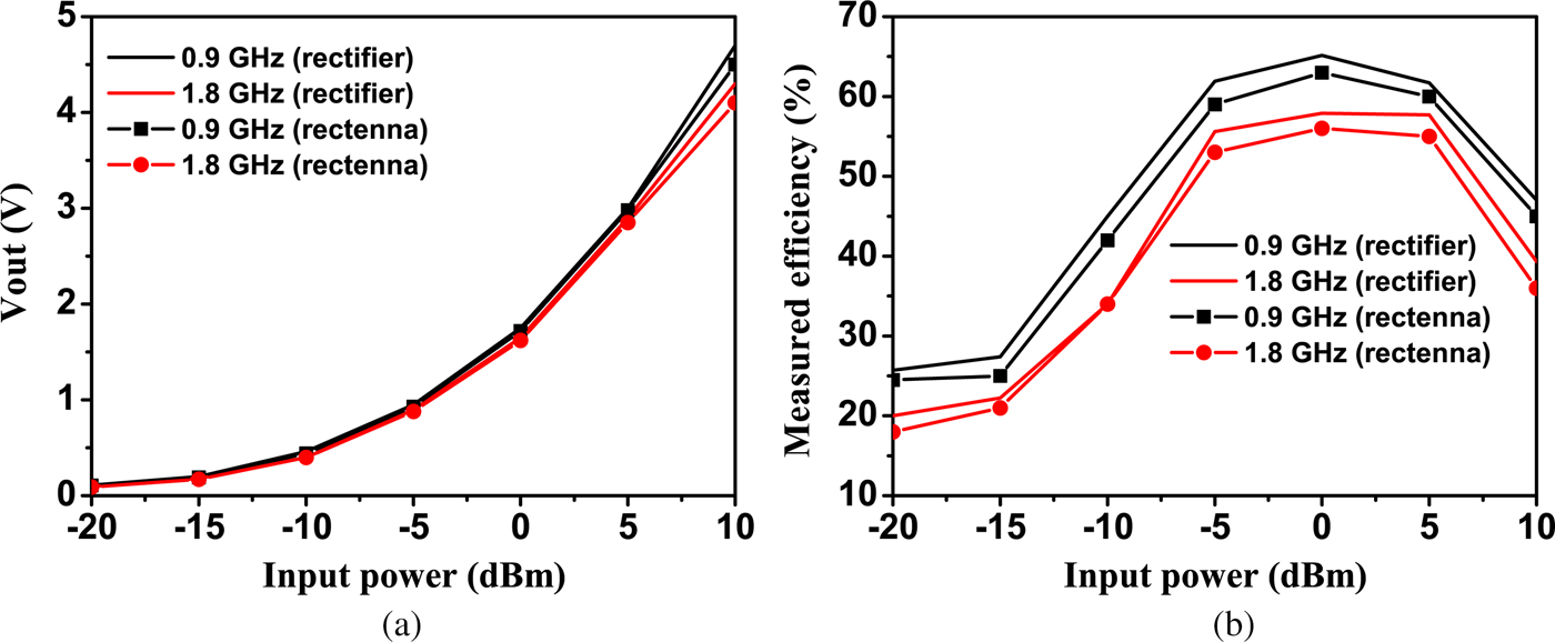
Fig. 11. Rectifier and rectenna measured (a) output voltage and (b) RF-to-dc efficiency.
A good agreement can be observed between rectifier's and rectenna's efficiency. At 0.9 GHz, rectifier efficiency is equal to 25.7 and 65.1% for an input power of −20 and 0 dBm, respectively, whereas the rectenna efficiency is equal to is 24.5 and 63%, respectively. From the figure it is also observed that both the rectifier and rectenna efficiencyat 1.8 GHz is <1.9 GHz that might be due to the increased parasitic losses in the rectifier diode. Figure 12 shows the rectifier output voltage for various input power levels and fixed the load resistance value of 4.7 kΩ. It can be seen that the maximum output voltage is achieved in the frequency range of 860–900 and 1770–1800 MHz, showing the rectenna's capability to harvest RF energy in the GSM-900 and GSM-1800 bands. Table 1 shows the comparison of the proposed work with the earlier reported works in terms of antenna type, bandwidth, rectifier, and rectenna's efficiency. As can be seen that the proposed rectenna system achieves the highest antenna bandwidthand reasonable RF-to dc conversion efficiency.

Fig. 12. Measured voltage versus frequency.
Table 1. Comparison of the proposed rectenna with recently published papers.

NS, not specified; PS, proposed structure.
VI. CONCLUSION
In this paper, a hybrid broadband PDRA has been proposed for dual-band rectenna system. The measured results of gain, radiation pattern, and impedance bandwidth are presented to validate the design. The result shows broad impedance bandwidth of 110.8% (0.86 to 3 GHz) and a stable radiation pattern. In addition, the antenna offers the maximum gain of 6.8 dBi and efficiency <90% over the frequency range of 0.9–2.7 GHz. Furthermore, to realize the dual-band rectenna system the proposed antenna is integrated with a hybrid dual-band rectifier circuit. The measured result demonstrated that the rectenna system provides an RF-to-dc conversion efficiency of 24.5 and 63 % for an input power of −20 dBm and 0 dBm, respectively. Besides, the proposed antenna is simple, easy to fabricate and has high radiation efficiency and stable radiation pattern, which make it robust and suitable candidate for other wireless communication applications.
 Sachin Agrawal did his M.E. from Birla Institute of Technology Pilani, India in 2009. He is currently pursuing his Ph.D. from PDPM-Indian Institute of Information Technology Design and Manufacturing Jabalpur, India. His areas of interest are RF Energy Harvesting, Antenna Designing, and Mobile Communication.
 Manoj Singh Parihar did his B.Tech. and M.Tech. from RGPV Bhopal in 2001 and 2004, respectively. He completed his Ph.D. from Indian Institute of Technology Delhi in 2012. He was a Senior Project Scientist in Center for Applied Research in Electronics, IIT Delhi from July 2010 to March 2013. In October 2007, he received “Institute of Electronics & Telecommunication Engineers (IETE) Research fellowship” for continuing his research work in Reconfigurable Antennas. He was a recipient of the travel grant (2007) awarded jointly by the National Institute of International Education (NIIED) and Republic of Korea. Currently, he is working as an Assistant Professor in IIITDM, Jabalpur. His areas of interest are Reconfigurable Antennas, Microwave Integrated Circuits, Microwave & Millimeter Wave device characterization, and RF MEMS.
 Pravin N. Kondekar did his B.E. from Pune University, M.Tech. from IISc Bangalore, and Ph.D. from IIT Bombay, India in 1983, 1989, and 2003, respectively. Currently, he is a professor in ECE discipline in IIITDM, Jabalpur India. His research interests include micro-electronics, VLSI-CMOS level design, nano-electronics devices, and semiconductor power devices.