I. INTRODUCTION
With increase in requirement of planar devices for various applications in communication systems, the microstrip antenna has attracted the attention of researchers. The microstrip antennas have several advantages in comparison to conventional antennas including their light weight, small size, availability in different shapes, ease of fabrication, and easy integration with other circuit components. Microstrip antenna, in general, consists of a radiating conducting patch and a conducting infinite ground plane separated by a thin dielectric substrate. However, such structures intrinsically have low gain, polarization impurity, and narrow bandwidth. Usually, broadband performance is a necessary requirement for modern communication systems hence these antennas in conventional form are not finding much application in consumer market. Looking at present requirements of communication systems, size reduction and bandwidth improvement are important parameters and due consideration is given in recent times for their improvement [Reference Garg, Bhartia, Bahl and Ittipiboon1, Reference Wong2].
Ultra-wideband (UWB) microstrip antennas are in great demand for applications in modern communication systems, wireless communication systems, and biomedical systems [Reference Schantz3, Reference Ray, Ranga and Gabhale4]. As per Federal Communications Commission, bandwidth for UWB applications extends from 3.1 to 10.6 GHz [5]. Recently, several techniques have been reported to obtain wideband behavior of the antennas such as introducing different shape slots in the patch and ground plane, use of stacked elements, and different feeding techniques [Reference Denidni and Rao6–Reference Rawat and Sharma9]. The commonly used geometries like rectangular, ellipse, and circular structures with modifications have been widely analyzed for UWB applications [Reference Sadat, Fardis, Geran and Dadashzadeh10–Reference Kang, Wu and Tarng12]. Many circular antenna designs have been investigated in past to obtain improved radiation characteristics, a circular microstrip antenna with off-centered y-slot is investigated [Reference Shekhawat, Sekra, Saxena, Saini and Bhatnagar13], it offers impedance bandwidth of 7.5% with circularly polarized performance. The gain is found to be around 3 dB in the entire bandwidth. In [Reference Bhatnagar, Saini, Saxena and Joshi14], a circular patch antenna with diamond cut slot is presented, the proposed antenna provides impedance bandwidth of 13.58%. For Radio frequency identification (RFID) applications, a compact wideband dual-frequency microstrip antenna is proposed [Reference Tiang, Islam, Misran and Mandeep15], using an offset microstrip-fed line and a strip close to the radiating edges, it offers dual frequency with the impedance bandwidth of 26.2 and 22.2%, respectively.
Annular ring microstrip patch antenna (ARMSA) is also a useful shape to be considered for study, mainly because of its high radiation performance. The presence of edges at the inner and outer radii causes development of more fringing field as compared to circular geometry, in which fringing occurs only at the outer edge. The bandwidth achieved by an annular ring for certain value of the radii is higher than that of a circular patch [Reference Chew16]. Moreover, the annular ring is more compact in size for a given mode of operation and at a given frequency than that of the rectangular or circular counterpart. To improve bandwidth in annular ring antenna various techniques like use of stacked patches, shorting pin, and different feeding methods have been suggested in literature [Reference Xi, Lin and Min17, Reference Ding, Yu and Zhang18]. ARMSA, which has conical radiation patterns, is suited to the applications of satellite communication and navigation also [Reference Chen, Li, Fu and Yan19]. Currently, defected ground microstrip patch antennas have been used for broadband applications in communication systems. In a defected ground structure technique, a defect is introduced intentionally in the ground structure of the microstrip antenna to achieve desired radiation performance. The benefit of using defected ground is that spurious surface wave excitation is less and even the low dielectric substrate does not support higher order mode. The shape and size of the defect is optimized, resulting in a controlled excitation and propagation of electromagnetic radiation through the antenna [Reference Guha, Biswas and Antar20–Reference Kandwal, Sharma and Khah23].
In this paper, investigation of the performance of an annular ring microstrip antenna with finite ground is carried out to obtain an impedance bandwidth of 52.02% within the UWB frequency range of 3.1–10.6 GHz. The performance of antenna is compared with that of a conventional circular patch and parameters like reflection coefficient, bandwidth, gain, radiation patterns, and voltage standing wave ratio (VSWR) are studied for the proposed geometry.
II. ANTENNA DESIGN AND RESULTS
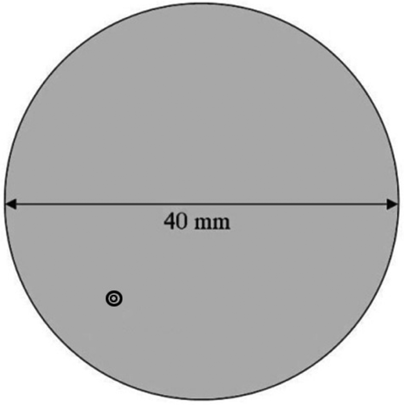
The configuration of conventional circular patch antenna having radius equal to 20 mm is shown in Fig. 1. The circular geometry is designed and simulated on glass epoxy FR-4 substrate having relative permittivity ε r = 4.4, substrate thickness h = 0.159 cm, and loss tangent tan δ = 0.025. The antenna is excited through probe feed arrangement associated with 50 Ω feed line. The simulated variation of reflection coefficient (S 11) of this single layer circular geometry as a function of frequency is shown in Fig. 2. This antenna resonates at a single frequency (f r = 6.03 GHz) and offers impedance bandwidth of nearly 2.34%. The simulated VSWR value corresponding to the resonant frequency is 1.08 and input impedance of antenna at the resonance frequency is (42.23 + j8.25) Ω. As the geometry exhibits narrow band characteristics, modification is needed to improve its impedance bandwidth.

Fig. 1. Simple circular geometry with feed.
Fig. 2. Variation of reflection coefficient (S 11) as a function of frequency.
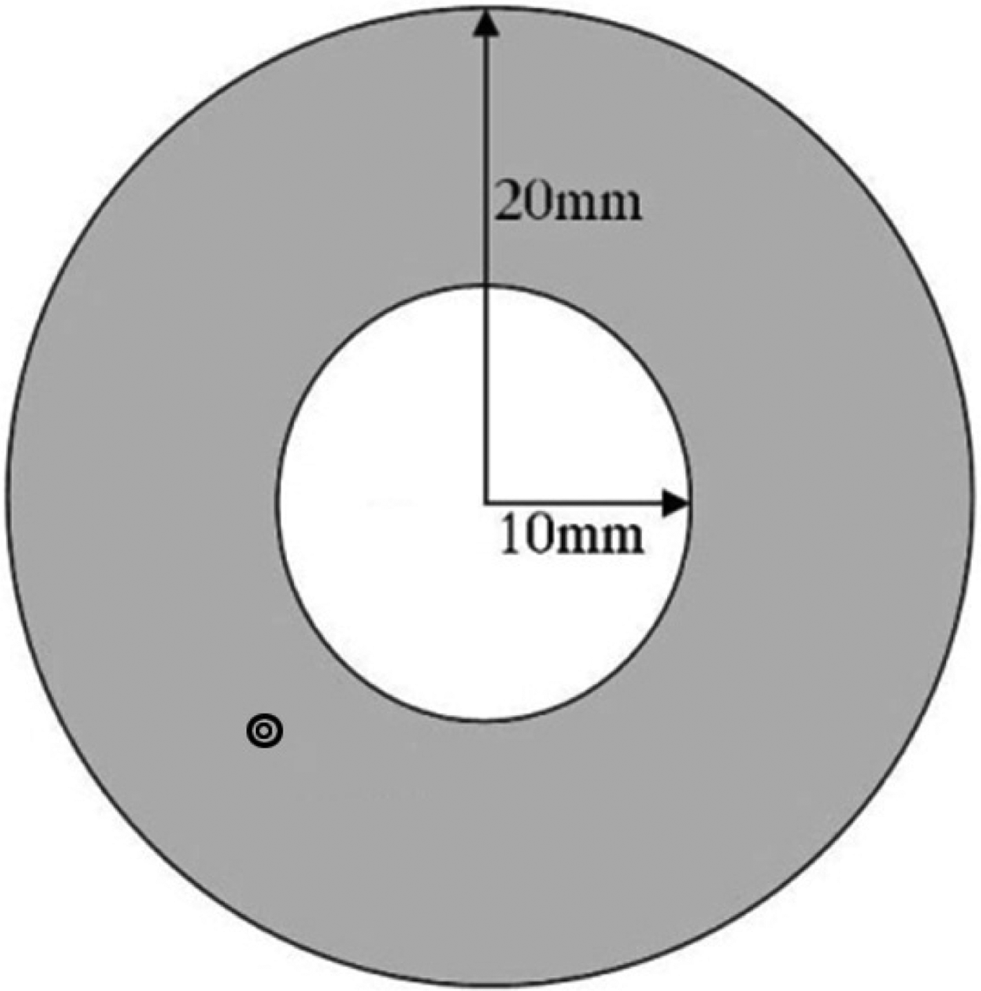
The next step of modification of antenna involves applying a circular slot of radius 10 mm in the previous considered circular patch geometry as shown in Fig. 3.
Fig. 3. Geometry of annular ring patch antenna with feed.
The simulated variation of reflection coefficient as a function of frequency is shown in Fig. 4 which indicates that antenna now has resonant frequency of 6.5 GHz. The resonance frequency of this modified antenna is slightly more as compared to circular geometry reported earlier (6.03 GHz) perhaps due to excitation of different modes. The simulated VSWR value at the resonant frequency is 1.05 which suggests fine matching between antenna and probe feed. The bandwidth of antenna is now increased to 23.27% which is 10 times more than that of earlier reported simple circular patch geometry. The input impedance at the resonance frequency is (53.05 − j2.506) Ω. The modified structure has improved impedance bandwidth but to achieve UWB behavior more enhancement in the bandwidth is required.
Fig. 4. Variation of reflection coefficient (S 11) as a function of frequency for annular ring.
III. ANNULAR RING DESIGN WITH DEFECTIVE GROUND
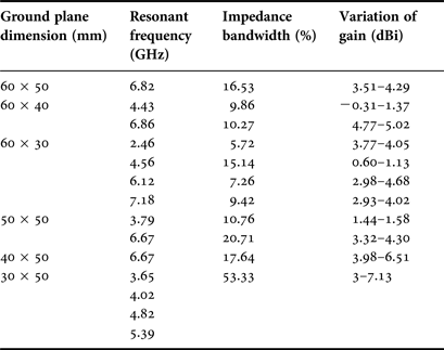
The antenna geometries described in preceding sections are further modified by making the ground size finite. The six considered finite ground plane dimensions and the results are reported in Table 1.
Table 1. Six different configurations of ground plane with results.
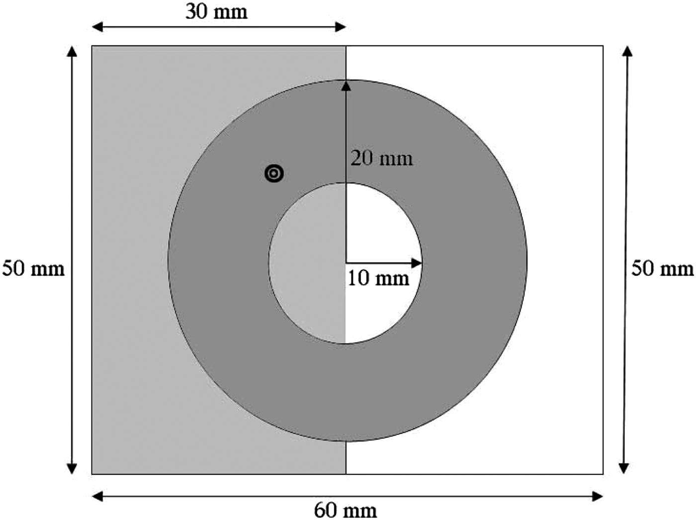
As indicated from Fig. 5, for ground size 30 × 50 mm, provide largest impedance bandwidth (53.33%). Furthermore, it also gives nearly uniform gain of around 4.5 dBi across the entire bandwidth as shown in Fig. 6. The geometry for reduced ground is shown in Fig. 7 and is considered for further analysis.
Fig. 5. Variations of reflection coefficient with frequency for six considered configuration.
Fig. 6. Variations of gain with frequency for six considered configurations.
Fig. 7. Top view of the proposed geometry with finite ground plane.
Such a reduction in ground plane yields lower band allocated for UWB applications which could not be achieved in previous two considered geometries. The fabricated prototype of proposed antenna geometry is shown in Fig. 8.
Fig. 8. Top and bottom view of fabricated prototype.
The simulated resonant frequencies of proposed geometry are 3.65, 4.02, 4.82, and 5.39 GHz while the measured resonant frequencies of this geometry are 3.708, 4.08, 4.94, and 5.45 GHz as shown in Fig. 9. It may be observed that the impedance bandwidth of antenna has now approached to 2.362 GHz (52.02%) corresponding to central frequency of 4.54 GHz. The measured VSWR values at four resonating frequencies are approaching to unity (1.28, 1.18, 1.41, and 1.53, respectively) which signifies that still antenna geometry has excellent match with the coaxial feed line as shown in Fig. 10.
Fig. 9. Measured and simulated reflection coefficient (S 11) with frequency for proposed geometry.
Fig. 10. Variation of measured and simulated VSWR as a function of frequency for proposed geometry.
The elevation radiation patterns of proposed single layered antenna at four frequencies within the impedance bandwidth region are shown in Fig. 11. It may be observed that the radiation patterns at all these frequencies are stable and maximum radiations are directed normal to the patch geometry.
Fig. 11. Variation of E and H plane elevation patterns at (a) 3.708 GHz, (b) 4.08 GHz, (c) 4.94 GHz, and (d) 5.45 GHz.
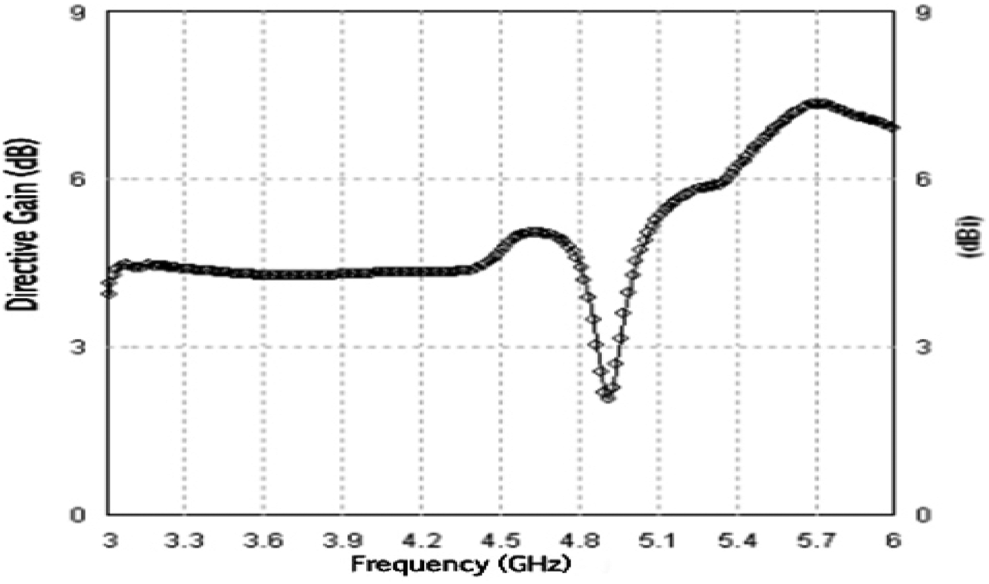
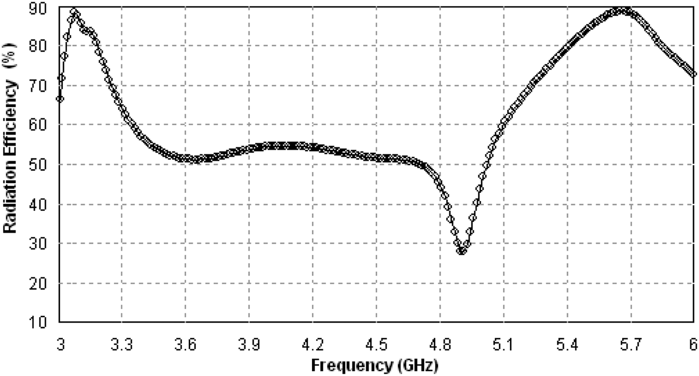
The variation of gain of the antenna with respect to frequency is shown in Fig. 12. It may be seen that from frequency 3 to 4.92 GHz, i.e. in the frequency range having first three resonance frequencies, gain of antenna is more or less constant and has value close to 4.5 dB. Thereafter for a narrow range of frequency, i.e. from 4.8 to 5.06 GHz, reduced gain is realized and subsequently the gain of antenna increases again. The gain of antenna at the fourth resonance frequency of 5.39 GHz is close to 6 dB. The radiation efficiency of proposed geometry is shown in Fig. 13 which is close to 50% for the entire bandwidth except from 4.72 to 5.01 GHz reduced efficiency is obtained. The performance of antenna in the lower band allocated for UWB communication systems is stable and this compact size antenna could be a better choice for UWB applications.
Fig. 12. Variation of gain with frequency for proposed antenna.
Fig. 13. Variation of radiation efficiency with frequency for proposed antenna.
IV. CONCLUSIONS
The performance of an annular ring microstrip antenna with finite ground is proposed in this paper. The results indicate that proposed antenna has 52.02% impedance bandwidth ranging from 3.3 to 5.7 GHz and good radiation characteristics in the operational band. This makes the antenna a potential candidate for variety of the communication applications. It is also demonstrated through parametric analysis that the size of ground plane has significant effect on the radiation characteristics of the proposed geometry.
Sanyog Rawat did Bachelor of Engineering in Electronics and Communication Engineering and Master of Technology in Microwave Engineering. Presently, he is working as Assistant Professor at Amity School of Engineering and Technology, Amity University Rajasthan. He is also pursuing Ph.D. in the field of Microstrip Patch Antenna from Malaviya National Institute of Technology, Jaipur. His research interest includes planar circuits, microwave devices, and circuits.
K.K. Sharma is working as Professor in Electronics and Communication Engineering Department of Malaviya National Institute of Technology, Jaipur. He did B.E. and M.E. from MREC, Jaipur and Ph.D. from IIT, Delhi. His research interest includes signal and image processing, and EMI/EMC.