I. INTRODUCTION
The microstrip antenna has been investigated extensively and applied in the various fields such as the mobile telecommunication and satellite wireless communication [Reference Sarin, Nassar and Deepu1–Reference Sun, Fang and Lin4], due to its excellent advantages, low profile, ease of fabrication, and light weight. Nevertheless the microstrip antenna is a kind of antenna with a narrow bandwidth and low gain. Lots of techniques has been reported to enhance the bandwidth and the gain for the microstrip antenna, such as shorted patch [Reference Malekpoor and Jam5, Reference Wu, Yin and Wang6], aperture loading [Reference Prabhakar, Kummuri and Yadahalli7, Reference Hu, Chen and Chu8] as well as multiple-layered substrate [Reference Liu, Kooi and Li9–Reference Tran and Park11]. The dual-layered substrate is considered as an effective approach to improve the radiation gain and enhance impedance bandwidth simultaneously [Reference Chen12]. As one layer substrate, the metasurface has attracted great attention of the researchers and engineers in the microwave devices design. The metasurface is a two-dimensional equivalent of the metamaterials [Reference Holloway, Kuester and Gordon13], and it is composed of the identical patches printed periodically on the surface of the substrate. Note that the dimension of the unit cell is required to be much smaller than the wavelength. Many metasurface-based antennas have been improved in terms of the radiation gain and impedance bandwidth. The metasurface is also capable to convert the linear polarization to the circular polarization [Reference Zhu, Cheung and Chung14–Reference Wu, Li and Li16]. In ref. [Reference Wu, Li and Li16], the proposed antenna has a high gain of larger than 5.20 dBi, a wideband of 46.9%, but height of the antenna is h = 5.77 mm (0.77λ 0) and the antenna is composed of triple different substrates with the same dimension and various dielectric parameters, which leads to the high cost. Another dual-layered substrate antenna is proposed in ref. [Reference Chen17], the −10 dB impedance bandwidth and −3 dB axial ratio bandwidth is reached up to 33.7 and 16.55%, respectively. The high gain is bigger than 5.8 dBi, and the height of the antenna is h = 4 mm (0.77λ 0). Compared with the antenna reported in ref. [Reference Wu, Li and Li16, Reference Chen17], the profile of the proposed antenna has been reduced further h = 3.2 mm (0.04λ 0), and the operating principle has also been illustrated by means of numerical simulation. The proposed antenna has the wideband 27% and high gain of 5.62–6.52 dB. It seems that the metasurface is equivalent to the parasitic elements in the antenna design.
In this paper, a dual-layered substrate high gain wideband microstrip antenna is investigated. The presented antenna is mainly composed of two sections, the driven patch and parasitic structure. The driven patch is a rectangular metal structure printed on the surface of the nether substrate. The parasitic structure is the four identical dual-breached circular patches printed on the surface of the substrate, which is the main radiation structure. The parasitic structure has the same performance as the metasurface in term of the impedance bandwidth enhancement and the radiation gain improvement. In order to seek the operating principle of the proposed antenna, two reference antennas with two different parasitic elements have been analyzed. The commercial software HFSS 13.0 is employed in the antenna design and optimization, the optimized antenna is fabricated for experimental measurement. The return loss, radiation efficiency, and the gain have been investigated for both the reference antenna and the proposed antenna, and the radiation pattern is studied only for the proposed antenna. We found that the simulated and experimental results are in good agreement and the impedance bandwidth is 27.0% (3.30–4.33 GHz), which is appropriate to be applied in the near future 5G wireless communication (3.30–3.40 and 3.40–3.60 GHz) or WiMAX (3.40–3.69 GHz).
II. ANTENNA CONFIGURATION AND ANALYSIS
A) Antenna design
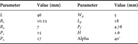
The configuration, the cross-section view and coordinate system of the proposed wideband high gain microstrip antenna with four metal parasitic elements printed on the upper surface of the substrate are shown in Fig. 1(a) and the prototype for the experimental measurement are shown in Fig. 1(b). The dimensions of the proposed antenna are listed in Table 1. The metal patches are printed on the surface of the FR4 substrate with the dielectric parameter of 4.4 and loss tangent of 0.02. The dual substrates have the same dimension of L × L × h (0.5λ × 0.5λ × 0.018λ), which are closely arranged together without any airspace.
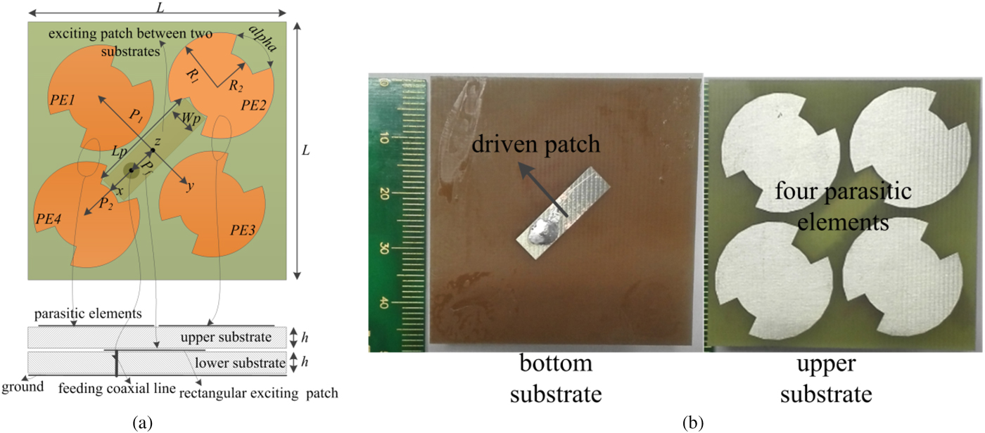
Fig. 1. (a) Perspective view and cross section of the proposed antenna (b) prototype of the proposed antenna.
Table 1. The dimension of the proposed antenna shown in Fig. 1.

Four circular parasitic patches with dual arced breaches at the symmetrical edge are fabricated on the surface of the upper substrate. For ease of description, they are denoted as the PE 1, PE 2, PE 3, and PE 4, respectively as shown in Fig. 1(a). The distance between PE 1 and PE 3 is 2P 1 = 30 mm, which is different from that 2P 2 = 34 mm between PE 2 and PE 4, and the centers of the circular patches are all located in the diagonal lines of the square substrate. A rectangular patch acting as the driven patch is printed on the upper surface of the lower substrate and its edge is not parallel to the edge of the substrate, instead, it is parallel to the diagonal line shown in Fig. 1(a). A 50 Ω coaxial line through the lower substrate and ground plane is used to excite the drive rectangular patch. The energy is coupled from the driven rectangular patch to the parasitic elements then be radiated secondly by the four circular parasitic elements. Therefore the performance of the proposed antenna is mainly related to the parasitic elements, and the driven section also has a great impact on the radiation.
B) Antenna analysis
The dual reference antennas will be studied in this section, and the configurations of the reference antennas are shown in Fig. 2. The antenna with the PE 1 and PE 3 is defined as the ant_1, and the antenna with PE 2 and PE 4 is denoted as the ant_2. Both reference antennas have been numerically simulated and the results are depicted in Fig. 3, It can be seen that ant_1 resonates at the frequency of 4.00 GHz and the impedance band ranges from 3.72 to 4.09 GHz, the radiation efficiency is larger than 75.0%, the gain is bigger than 5.61 dBi throughout the impedance bandwidth. The operating band of the ant_2 is from 4.12 to 4.34 GHz, and the radiation efficiency is larger than 74.1%, the gain is bigger than 6.05 dBi over the band. The resonance frequency of the ant_2 with good matching is 4.25 GHz, and both resonance frequencies are same to the second and third resonance frequency of the proposed antenna. Figure 3(a) shows another resonance frequency but a worse matching around 3.45 GHz which is agreed with the first resonance frequency of the proposed antenna. It can be concluded that the broadband is from the combination of the three resonance frequencies which is generated by the ant_1 and ant_2 respectively. For the ant_1 and ant_2, the two circular parasitic elements have the same dimension, and the unique difference is the location of the parasitic elements relative to the driven patch, then the different resonance frequencies are produced. The polarization of the ant_1 and ant_2 is the linear polarization mode, which is same to the proposed antenna.
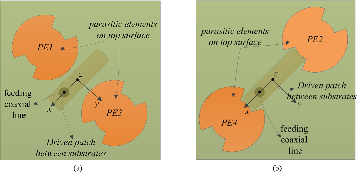
Fig. 2. Reference antenna with the partial parasitic elements (a) PE 1 and PE 3, (b) PE 2 and PE 4 as the main radiation structure.
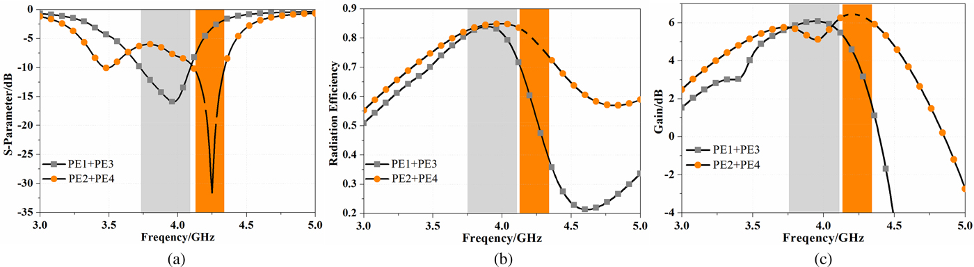
Fig. 3. (a) Reflection coefficient (b) radiation efficiency, and (c) peak gain of both ant_1 and ant_2.
III. SIMULATION AND EXPERIMENT RESULT
The proposed high gain wideband microstrip antenna is numerically simulated and optimized using the commercial electromagnetic simulated software HFSS, meanwhile, the prototype shown in Fig. 1 has been experimentally researched in detail in terms of the S-parameters, radiation pattern, radiation efficiency and peak gain in the following.
A) Parameters analysis
The radiation performance of the antenna is greatly dependent on the dimension of the antenna, especially the resonance frequency. the S-parameter of the proposed antenna is illustrated in Fig. 4 as the alpha, R 1, R 2, and L p are assigned to the different values. From Fig. 4(a) it can be seen that that as the value of the alpha varies from 15.0° to 25.0°, three resonance frequencies shift to the higher frequency, the distance between the different resonance frequencies becomes closer, and the port matching becomes worse at the resonance frequencies. We can see from Fig. 4(b) that the second resonance frequency disappears when L p = 17.0 mm, the first resonance frequency moves to the lower frequency but the third seems to be stable as the value of the L p varies from 17.0 to 18.5 mm. The effect of the R 1 on the proposed antenna is shown in Fig. 4(c), the three resonance frequencies move to the lower frequency as the R 1 is assigned from 9.5 to 10.5 mm, and the port matching has been improved. The effect of R 2 is similar to the R 1, the larger value leads to the lower resonance frequency, and inverse in Fig. 4(d), the porting matching especially in the middle of the two resonance frequency becomes worse as the R 2 is assigned to the larger values. All of the above geometrical parameters can be used to optimize the proposed antenna, and the analysis of them can help us to find out the principle of the resonance.

Fig. 4. Influence of the geometrical parameters on the return loss of the proposed antenna, (a) effect of alpha, (b) effect of L p, (c) effect of R 1, (d) effect of R 2.
B) S-parameters
The simulated and measured S-parameter of the proposed antenna is shown in Fig. 5 and the tested S 11 is carried out by Agilent PNA Series Network Analyzer E8363B. It is clearly shown that the wide impedance bandwidth is from the combination of the three resonance frequencies and good matching is achieved at these frequencies. The wide bandwidth (S 11 < −10 dB) from 3.30 to 4.32 GHz (1.02 GHz, 26.8%) covers both the 5G band (3.30–3.60 GHz) and WiMAX band (3.40–3.69 GHz). The good port matching is acquired by regulating the position of the exciting port relative to the driven patch since the different place has the different impedance. The optimized impedance is acquired as the exciting port is positioned to (4.5 mm, 0) relative to the coordinate system shown in Fig. 1(a).
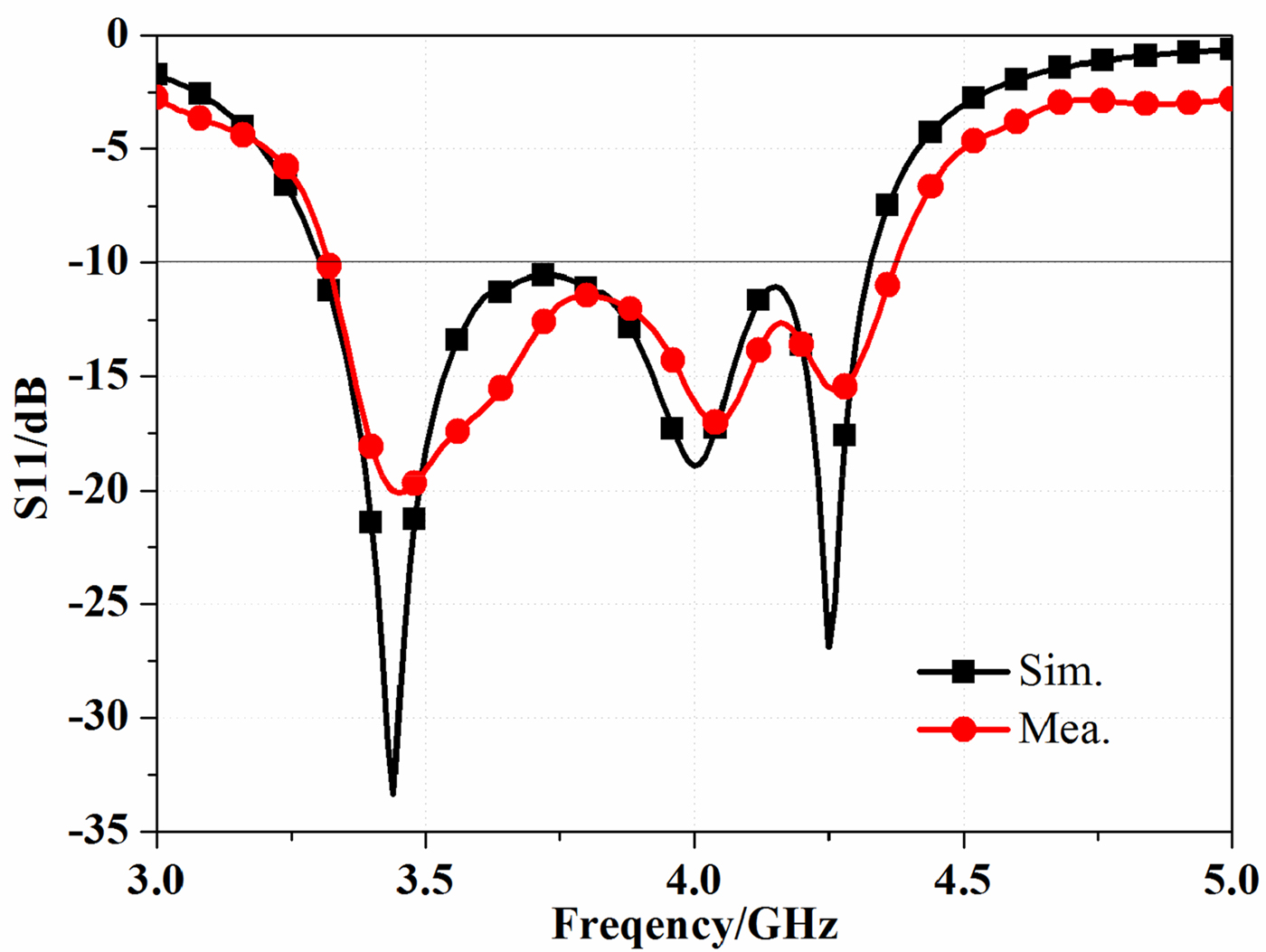
Fig. 5. The simulated and measured reflection coefficient of the proposed microstrip antenna.
The simulated and measured results are agreed with each other, and the little discrepancies are due to the measurement or the fabrication tolerance, such as the poor connection between inner core of 50 Ω SMA connector and the rectangular exciting patch, the air layer existing between the dual substrates.
C) Radiation pattern
The radiation characteristics of the proposed antenna have been simulated and measured using the HFSS and anechoic chamber respectively. The radiation patterns for the proposed antenna at two main planes (xoz- and yoz-planes) and at frequencies of 3.44 GHz, 4.00 GHz as well as 4.25 GHz are plotted in Fig. 6. The frequencies (3.44, 4.00 and 4.25 GHz) are chosen since the proposed antenna resonates at these frequencies shown in Fig. 5. The presented antenna radiates mainly towards the perpendicular direction of the patch plane, which is completely agreed with the theoretical principle of the plane antenna. The radiation pattern in xoz-plane is the co-polarization radiation pattern, and the one in yoz-plane is the cross-polarization radiation pattern relative to the coordinate system shown in Fig. 1(a). The cross polarization discrimination is extremely tiny especially in the maximum radiation direction which accounts for a good polarization purity along the x-axis. The simulated and measured results are agreed with each other, although the less smooth tested results are probably caused by the testing process in the anechoic chamber or the manufacturing errors.

Fig. 6. The simulated and measured radiation pattern of the proposed antenna at different frequencies and two orthogonal primary planes (a), (b) f 0 = 3.44 GHz (c), (d) f 0 = 4.00 GHz (e), (f) f 0 = 4.25 GHz.
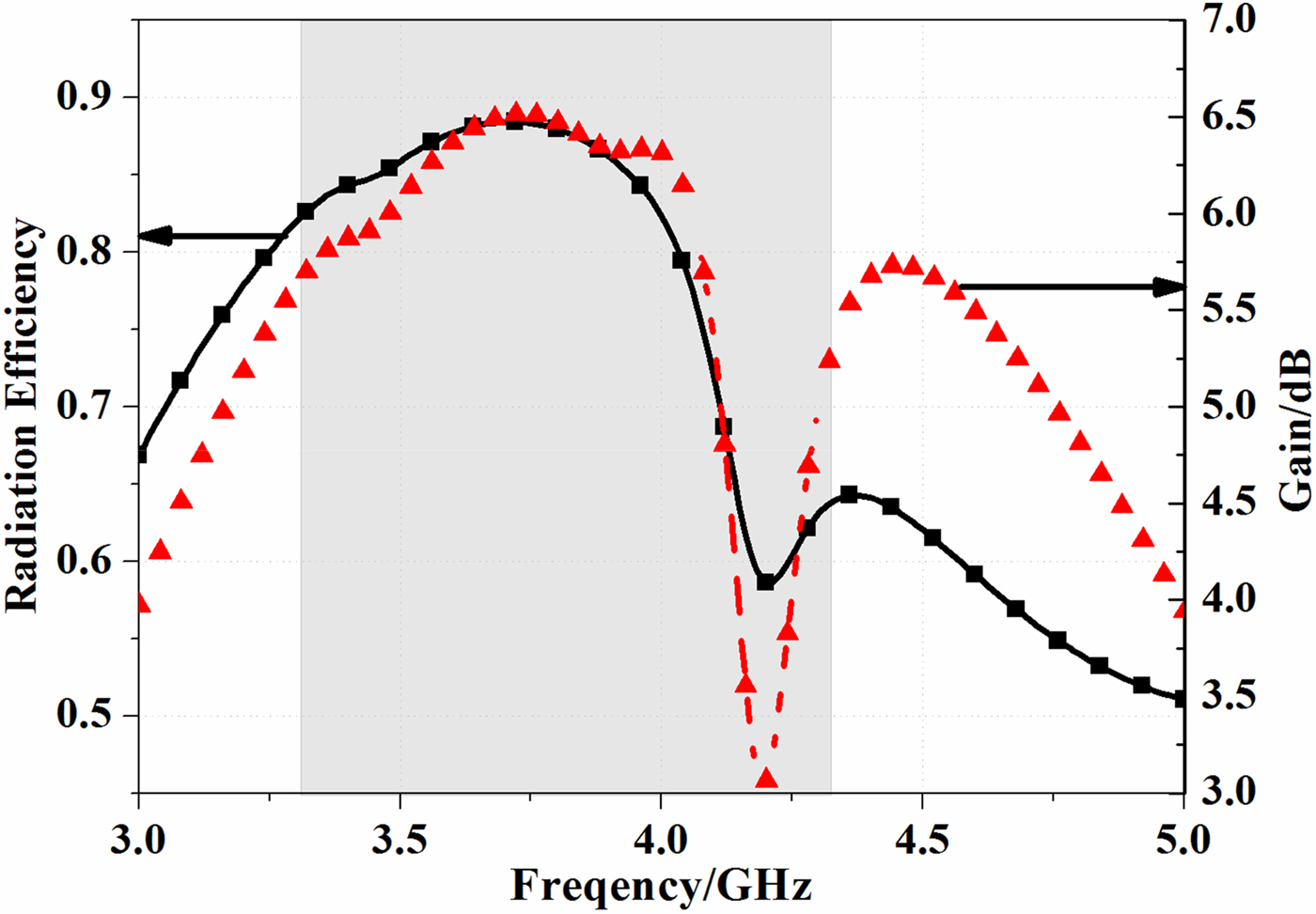
D) Radiation efficiency and gain
The measured radiation efficiency and the peak gain of the proposed antenna are depicted in Fig. 7. The figure shows that both of them extremely decline around the frequency of 4.20 GHz, which is resulted from the opposite direction of the vector surface current on the PE 1, PE 3, and PE 2, PE 4. But in the 5G band (3.30–3.60 GHz) or WiMAX band (3.40–3.69 GHz), the radiation efficiency is bigger than 81.9% and peak gain is larger than 5.62 dBi, the maximum values are reached up to 88.4% and 6.52 dBi which are well suitable to be applied practically.

Fig. 7. Measured radiation efficiency and gain of the proposed microstrip antenna.
VI. CONCLUSION
A wideband high gain dual-layered substrate microstrip antenna is proposed in this paper. Four breaches circular patches on the surface of the upper substrate as the main radiation structure are considered as the parasitic structure rather than the metasurface since they are aperiodic. Two reference antennas with two of the parasitic elements are investigated to illustrate the principle of the proposed antenna, which offers a good reference to the dual-layered microstrip antenna design. The proposed linear polarization microstrip antenna operates in the band ranging from 3.30 to 4.33 GHz which covers the 5G/WiMAX wireless communication specification, and the radiation pattern in three different frequencies has not been deformed unlike the higher mode of the single patch. It is capable to be applied in the 5G/WiMAX wireless communication system in the near future.
ACKNOWLEDGEMENT
This research has been supported by the fund of space innovation and the authors also thank sincerely the anonymous reviewers for their constructive comments which helped to substantially improve the quality and presentation of this manuscript.
 Haixiong Li was born in Shannxi Province, China, in 1982. IEEE Student Member, CIE Student Member. He received the B.Sc. degree in School of Electrical Information Science & Engineering, Lanzhou University in Lanzhou city, China, in 2006. He received the M.Sc. degree in School of Information Science and Technology, Xiamen University in Xiamen city, China in 2013. He is presently working on his doctoral degree in School of Electronics and Information, Northwestern Polytechnical University in Xi'an city, China. His research interests include Electromagnetic Metamaterials and MIMO antenna design.
 Bozhang Lan was born in shannxi Province, China, in 1992. He received the B.S. degree in electronic science and technology from HeFei University of Technology in HeFei city, China, in 2014, and received the M.S. degree in electromagnetic field and microwave technology from Northwestern Polytechnical University in Xi'an city, China, in 2016. He works for Ph.D. degree in Northwestern Polytechnical University. His research interests include: reconfigurable antenna, microwave filter.
 Jun Ding was born in shannxi Province, China, in 1964. She received the M.Sc., B.Sc., and Ph.D. in School of Electronics and Information, Northwestern Polytechnical University in Xi'an city, China, in 1986, 1989 and 2005 respectively. She is a professor in School of Electronics and Information NWPU. She has published more than 100 research papers. Her research interests include; Electromagnetic Metamaterials, the antenna theory and design, and the microwave circuit design.
 Chenjiang Guo was born in shannxi Province, China, in 1963. CIE Senior Member, Antenna Society Committee Member. He received the M.Sc. B.Sc. and Ph.D. in School of Electronics and Information, Northwestern Polytechnical University in Xi'an city, China, in 1984, 1987 and 2007 respectively. He is a professor in School of Electronics and Information NWPU. He has published more than 140 research papers. He research interests includes; EMI/EMC, the antenna theory and design, and the microwave circuit design.