I. INTRODUCTION
A number of published papers have the objective to obtain multiband performance without paying much attention to provide wideband along with good radiation characteristics at each operating frequency [Reference Puente, Romeu, Pous and Cardama1–Reference Chayono, Haneishi and Kimura3]. Microstrip antenna (MSA) has many distinct features to make it most popular and widely used antenna, but it suffers from low-impedance bandwidth (BW), low-gain, and low-power handling capability [Reference Kumar and Ray4]. Antenna structures with good radiation characteristics and impedance characteristics are realized by arrays. Several other methods for obtaining multiband and wideband antenna characteristics have been developed. Dual wideband folded microstrip patch antenna was introduced for possible wireless local area network applications in 3–4 GHZ frequency range [Reference Sittironnarit and Ali5]. In [Reference Yang and Rahmat-Samii6], a novel reconfigurable patch antenna with switchable slots (PASS) was proposed to realize various functionalities, such as dual-frequency operation, circularly polarized (CP) performance, and polarization diversity with only one patch and a single feed. In [Reference Asrokin, Rahim and Abdelaziz7], a multiband MSA operating at different frequencies of 2.4 and 5.2 GHz was presented. In this dimensions of the single elements of the operating frequencies were calculated using the transmission line model. Two elements of an inset-fed MSA were used for each frequency band. Another way to improve the BW and achieve single-layer multiband characteristic is to create antenna with more patches or more extra components. In [Reference Vaidya, Gupta, Mishra and Mukherjee8], an efficient, high-gain antenna structure with low side-lobe level using parasitic patches has been introduced. In [Reference Abdelaziz9], a novel MSA with wideband is presented by adding two parasitic elements to one element of the proposed antenna. BW improvement along with low side-lobe level of reflectarray antennas has been achieved using closely spaced elements in [Reference Nayeri, Yang and Elsherbeni10]. In [Reference Kandwal, Chakravarty and Khah11], a circuital method to calculate the admittance of gap-coupled sectoral patch antenna with wideband has been introduced. When many antennas are packed into a small volume, other effects such as mutual coupling will become dominant. Mutual coupling is shown to de-correlate the signals at the antenna connectors in some cases [Reference Svantesson and Ranheim12–Reference Andersen and Lau15], and therefore may give a higher capacity than first expected. An additional effect of mutual coupling is that it changes the antenna impedance, which may lead to impedance mismatch if no matching network is used. Several papers have considered this effect [Reference Kildal and Rosengren16–Reference Yin, Ruan, Mo, Ding and Chu20]. Impedance mismatch is especially deleterious when the dominant signal impairment is receiver/amplifier noise. Impedance mismatch yields lower received signal power and therefore reduces receiver signal-to-noise ratio. Effect of variation of the size and position of a parasitic element with input impedance and BW has been investigated theoretically in [Reference Au and Luk21].
In this communication, we have introduced a new gap-coupled stacked sectoral patch antenna array, which uses parasitic elements placed near the active antenna element using high low dielectric constant substrates. In order to achieve wideband and multiband characteristics, the parasitic elements are placed near the vicinity of the active antenna element. This will add to in achieving wideband characteristic at the resonant frequencies along with multiband. Along with this, the antenna is further studied using a stacked structure where a different substrate has been used and therefore will add to the wideband characteristic.
II. SECTORAL ANTENNA CONFIGURATION AND DESIGN
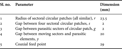
First a circular patch of radius 23.5 mm is designed. Then in order to enhance is antenna characteristics, gap-coupling technique has been applied. The circular patch is divided into first two sectors and then into four sectors. The gap between the parasitic elements has been optimized by various simulations. In order to further enhance the antenna properties, the concept of moving parasitic elements has been applied. This results in enhancement of impedance BW of the antenna along with improvement in the radiation properties such as antenna gain and side-lobe level. Further studies were carried out by arraying the structure. Similar geometry has been used for arraying. The gap between the antenna elements has been optimized and best possible results have been considered for further study. The gap study has been shown in the respective figures. Further in order to enhance the impedance BW, stacking of the layers of similar geometry has been done. Finally, a stacked-coupled geometry has been proposed which gives multiband along with wide impedance BW and good radiation characteristics. Resonant frequency of antenna is greatly affected by the dielectric constants of substrates used. In general, resonant frequency is inversely proportional to dielectric constant. When two different dielectric constant substrates are used, the overall constant increases and thus lowers down the resonant frequency as is clear from the graphs shown.
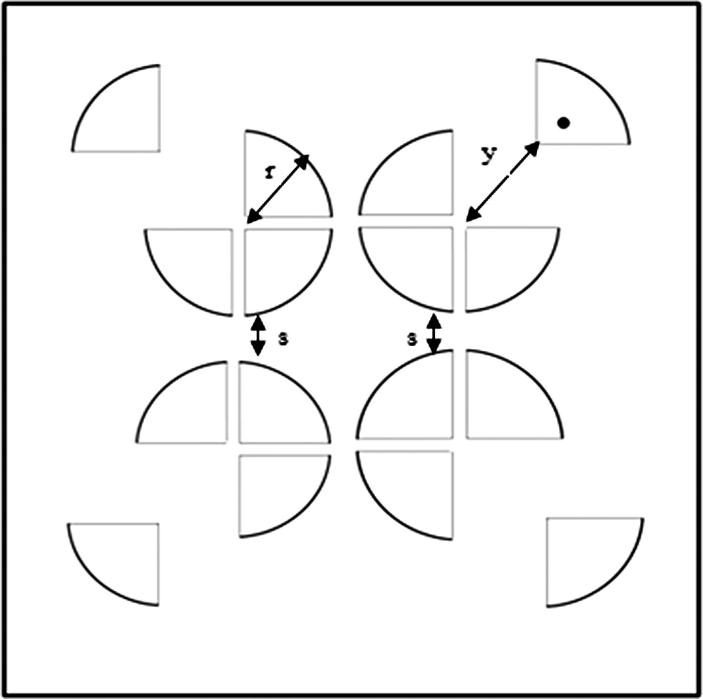
Figure 1 shows the geometry of the proposed antenna structure. Figure 2(a) shows the prototype of the proposed gap-coupled sectoral multiband antenna design with a square-shaped finite ground plane. Figure 2(b) shows the prototype of the proposed antenna structure with stacking. The design consists of four gap-coupled sectoral circular patch antennas with similar geometry placed along the four corners of a square. The proposed multiband antenna is printed on an FR4 substrate with permittivity of 4.4, a loss tangent of 0.024, and compact dimension of (140 × 140) mm2 (h = 1.59 mm). The antenna structure is coaxially fed at one of the circular sectoral antenna at a distance of 29 mm from its center as shown in Fig. 1 to achieve 50 Ω characteristic impedance. On the front surface of the dielectric substrate, four 3-mm-wide (gap in between four patches) sectoral antennas of similar geometries are printed.

Fig. 1. Geometry of the proposed antenna.
Fig. 2. (a) Prototype of the proposed single-layer antenna. (b) Prototype of the proposed stacked antenna using different dielectric substrates.
For further analysis of the proposed antenna structure, stacking is employed. The two substrates are connected using a coaxial feed from the bottom of ground plane to the excited patch. Moreover, the antenna is also tested using four connecting pins at the extreme edges, which hold the two substrates together with some gap. The geometry remains same at the upper layer except the substrate. The substrate used at the upper layer is Rogers/Duroid 5880 (lossless) having dielectric constant 2.2.
The antenna structure is analyzed theoretically, studied using two simulation software's CST studio suite and Ansoft HFSS 14.0 and experimentally measured using a vector network analyzer (9 kHz–13.6 GHz).
BW can be calculated using relation:
 $$BW\lpar \percnt \rpar =\displaystyle{{\lpar f_h - f_l \rpar } \over {f_c }} \times 100\comma \;$$
where, f h is the higher frequency, f l the lower frequency, and f c the central frequency  $= \displaystyle{{f_h+f_l } \over 2}.$
Resonant frequency varies with the dielectric constant as:
 $$f_r \alpha \displaystyle{1 \over {\sqrt {\varepsilon _r } }}\comma \;$$
where, f r and ε r are the resonant frequency and dielectric constant.
Antennas A and B have same dimensions and geometry and are symmetric. Variation is just in different dielectric substrates used.
Design specifications are tabulated in Table 1.
III. RESULTS AND DISCUSSION
The antenna performances were measured over the frequency range from 2.0 to 12.0 GHz. The results are verified used two commercially available simulation software's CST Studio Suite and Ansoft HFSS 14.0 whereas for experimental verification a vector network analyzer has been employed. We have added three parasitic elements of same geometry with the same patch layer having a finite ground plane.
Therefore, the four antenna element arrays have been structured in such a way that they form a square-shaped geometry including one active element and three parasitic elements.
BW enhancement can be achieved using closely spaced elements or using parasitic patches. Different approaches have been implemented in order to improve the BW of the antenna such as multilayered structures, single-layer multi-resonant designs, aperture-coupled designs, etc. The coupling between the elements is a function of the patch size and gap between the patches. The element spacing has a large influence on the array factor as well. Larger element spacing results in a higher directivity. However, the element spacing is generally kept smaller than λ/2 to avoid the occurrence of grating lobes. Mutual coupling between antenna elements is an important issue in the designing of antenna arrays. It significantly affects the antenna gain, directivity, and beam width of the antenna array. Therefore, mutual coupling can be utilized to achieve BW enhancement with desired performance of reflection coefficient and realized gain by cancelling the reflected waves from each element to the feeding network. Because printed slot antennas are promising candidate used in phased arrays, satellite communication systems, and airborne applications due to their compact size and high efficiency, two and four element slot arrays are used to study their mutual coupling and to demonstrate the BW enhancement by invoking suitable mutual coupling. Mutual coupling between array elements affects both the embedded element radiation patterns and the element input impedances.
Results obtained are shown below in sections.
A) Using single layer with dielectric constant 4.1
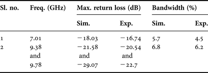
Figure 3 shows the return loss variation of the single layer parasitically coupled antenna using FR4 substrate with dielectric constant 4.1. Figure 3(a) shows study at different gaps of excited sector and feed positions. From this graph, it is clear that multiband is obtained but with no wide band. First two resonant frequencies are showing very low BW although good return loss. Figure 3(b) shows return loss at a gap of 20 mm at which good results are obtained. The antenna resonates in different frequency bands but the dominant resonant frequencies with good BW also are at 7.01 and 9.78 GHz. The antenna also shows dual resonance in X-band resonating at 9.38 and 9.78 GHz. A BW of 5.7 and 6.8 % has been obtained at two resonant frequencies, respectively, with a good agreement in simulated and measured results. A good return loss of −25 dB has been obtained at the first resonant frequency and −35 dB at the second resonant frequency.
Fig. 3. (a)Variation of return loss (dB) with frequency (GHz) using single-layer structure at different excited sector gaps. (b)Variation of return loss (dB) with frequency (GHz) using single-layer structure with excited sector gap of 20 mm.
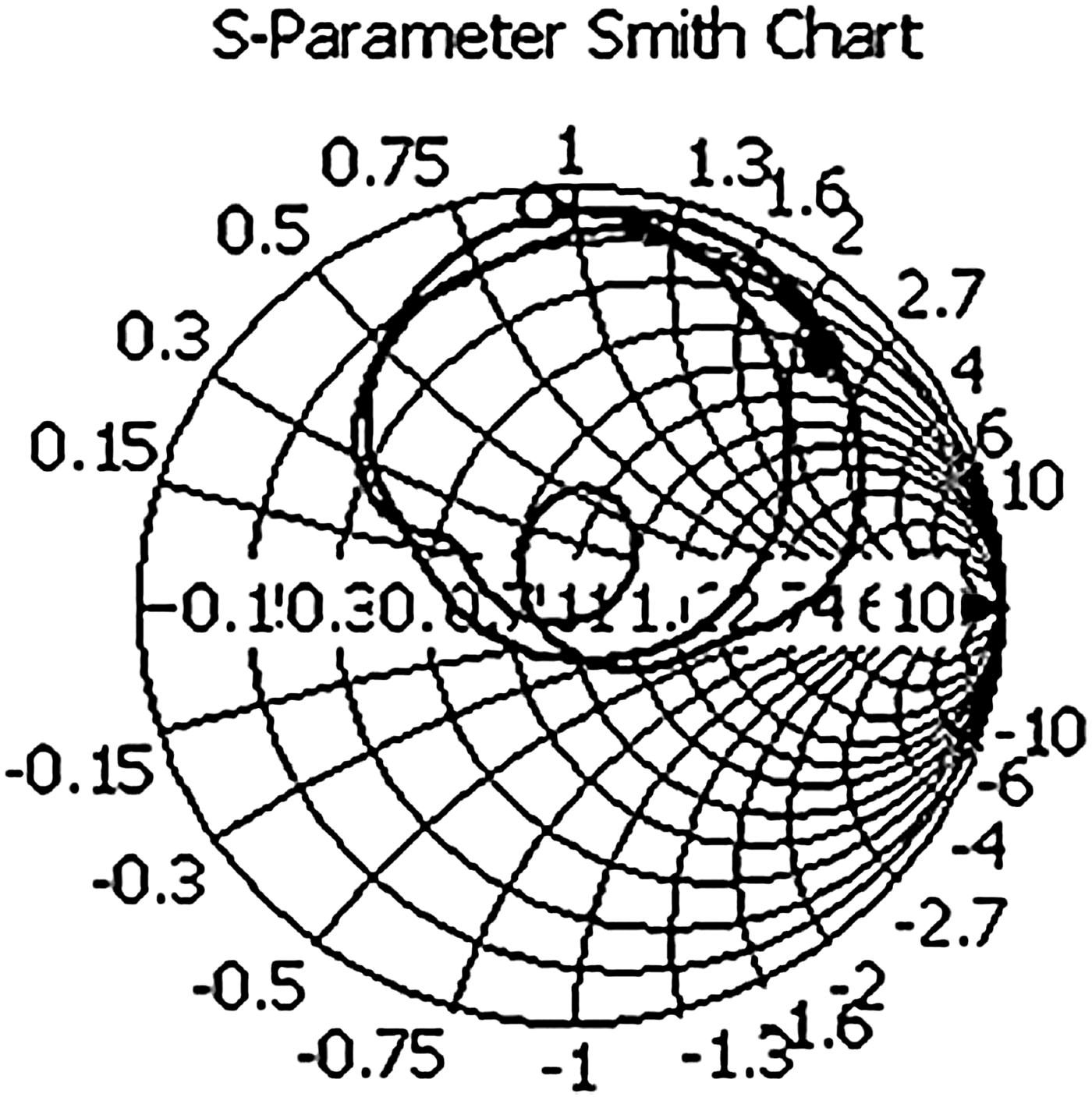
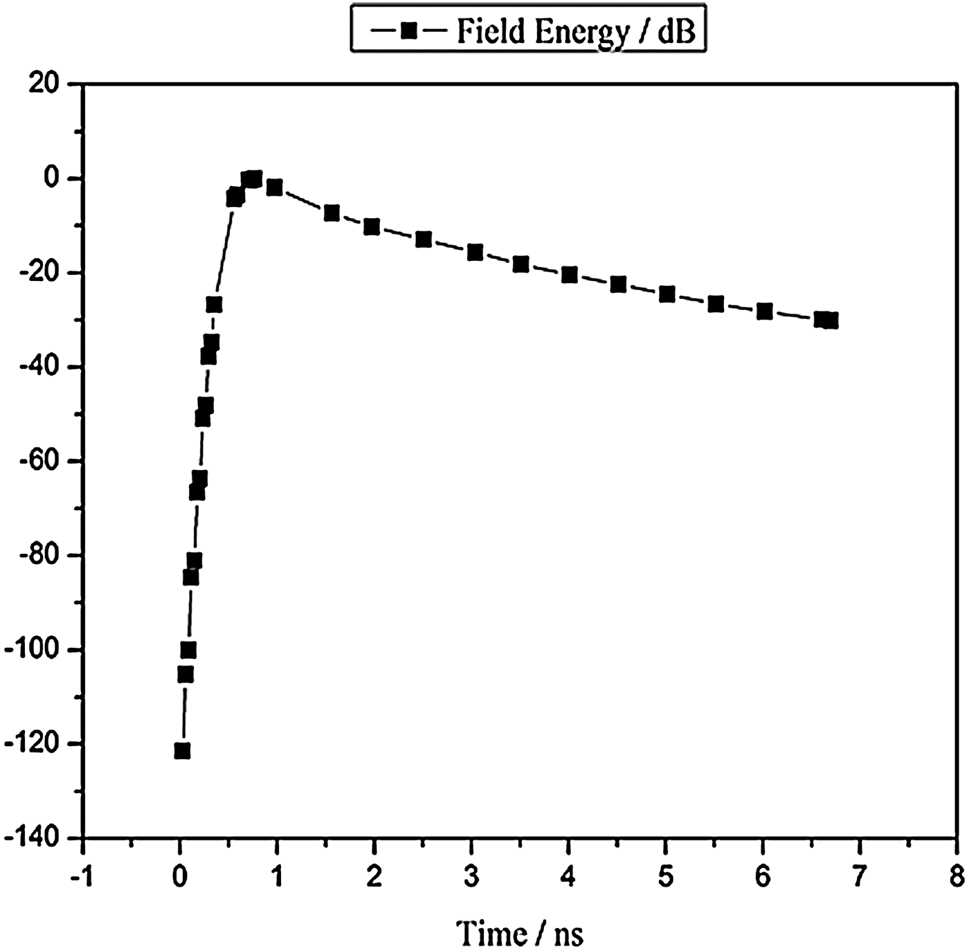
Figure 4 shows the smith chart graph for this antenna structure. Figure 5 shows the Cartesian plot of field energy variation with respect to time.
Fig. 4. Smith chart using single-layer structure.
Fig. 5. Variation of field energy/dB with time/ns using single-layer structure.
The results obtained are tabulated in Table 2.
Table 1. Design specifications.
B) Using stacked structure with dielectric constant 2.2 of the upper layer
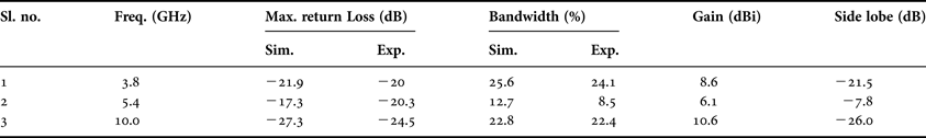
Figure 6 shows the S-parameters (S 11 in dB) of the proposed antenna array. The antenna resonates at three different frequencies: 3.8, 5.4, and 10.0 GHz. The simulated and measured results are therefore presented graphically and in good agreement with each other. At frequencies 3.8, 5.4, and 10.0 GHz, the antenna shows measured impedance BW of about 25.6, 12.7, and 22.8%, respectively. The graphs for input impedance are also shown in Figs 7(a) and 7(b). It can be analyzed from these graphs that the antenna shows a good impedance matching at the resonant frequencies.
Fig. 6. Variation of return loss (dB) with frequency (GHz) for stacked layer.
Fig. 7. (a) Variation of real input impedance (Ω) with frequency (GHz) for stacked layer. (b) Variation of imaginary input impedance (Ω) with frequency (GHz) for stacked.
Figures 8(a) and 8(b) show the radiation (far-field) patterns at the three resonant frequencies for single layer and stacked layer, respectively. A good antenna gain with low side-lobe level has been obtained. A maximum antenna gain of 10.6 dBi is obtained with a low side-lobe level of −26 dB for 3 dB angular width at resonant frequency of 10.0 GHz.
Fig. 8. Radiation pattern (far-field) at different resonant frequencies. (a) For single layer. (b) For stacked layer.
The results obtained for the proposed antenna design are therefore tabulated in Table 3.
Table 2. Results obtained for the single-layer antenna array.
Therefore, the proposed designed parasitically coupled stacked sectoral antenna array shows multiband and wideband characteristics along with high gain and low side-lobe level (Table 3).
Table 3. Results obtained for the stacked antenna array.
IV. CONCLUSION
The aim of the proposed coupled stacked sectoral array using high low dielectric constant substrates has been achieved. Antenna shows a multiband along with wideband characteristics. The effect of coupling, parasitic elements, and stacking has clearly been explained. The radiation (far-field) characteristics obtained shows that the antenna resonates with a good gain and very low side-lobe level. The effect of adding different dielectric constant substrates is therefore explained using the results obtained. Therefore, the proposed antenna design is very useful for different wireless communication systems such as mobile systems, satellite systems, and applied physics.
Mr. Abhishek Kandwal, received his M.Sc. degree in Physics from Himachal Pradesh University, Shimla, India, in the year 2009. He is presently pursuing Ph.D. His work includes the design and numerical modeling of wideband microstrip antennas. His field of interest includes designing and developing novel antennas with new numerical methods for wideband microstrip antennas for communication systems.
Mr. Jai Verdhan Chauhan, received his M.Sc degree in Physics Honors (Specialization in Electronics) from Delhi University, India in the year 2009. He is currently pursuing his PhD in Microstrip Antennas. His research includes design and simulation of shared aperture microstrip antennas and arrays along with numerical modeling for communication systems.
Prof. Sunil Kumar Khah, received B.Sc. (Electronic Sciences) from Kashmir University; M.Sc., M.Phil, and Ph.D. from Agra University. He was visiting Professor at University of Dayton, Ohio, USA in the year 2013–14. He did his postdoctoral research in the field of high power microwave component design. Presently, he is working as a professor in the field of Electromagnetics at Department of Physics, Jaypee University of Information Technology. Moreover, he is working on high efficiency low sidelobe level antenna design and wideband dual band antenna designs. His research interest is numerical modeling of high frequency antenna designs. He is life member of PSSI, MRSI, and member of IEEE.