I. INTRODUCTION
The performance of a modern radio frequency (RF) communication system is critically dependent upon an effective and careful design of a broad range of passive components, such as, power dividers, filters, couplers, phase shifters, antennas etc. While each of these components has an important role to play in the overall performance of the system, the importance of antenna cannot be overstated, since it acts as a bridge between the system and air which is the communication channel in wireless systems. As the wireless technology has grown, the task of antenna designer has become more and more arduous. Mobile and hand-held communication systems need small and light-weight antennas with high gain, large radiation efficiency, low profile, and tailored radiation pattern. Owing to their various advantages, like low profile, small size, and weight, low cost, easy conformability, compatibility with monolithic circuits, planar antennas have attracted tremendous research effort during the last three decades and are now commonly used in most communication systems.
Another consequence of the recent explosive growth in wireless technology is that the frequency spectrum has become a scarce resource and has to be efficiently utilized to accommodate various applications. A number of new wireless multimedia applications demand operation of the device at a number of frequencies. The antenna designers have responded to this demand in two ways – by designing planar multi-band antennas capable of operating at multiple frequencies and broadband antennas which can accommodate all the desired frequencies. Since microstrip antenna is inherently a narrowband device, a number of broadbanding techniques have been developed. The bandwidth of the microstrip antenna can be increased by using a thick dielectric layer. In this case, however, a coaxial feed cannot be used as it introduces a large inductive reactance which has to be tuned out to minimize impedance mismatch. To overcome this problem, a modified feeding technique has been presented in [Reference Fong, Pues and Withers1], where the inductive reactance of probe has been compensated by a lumped series capacitance incorporated into the element structure itself. Another common technique to increase the bandwidth is to use stacked patches. An aperture coupled stacked patch L-band antenna has been proposed in [Reference Targonski, Water House and Pozar2] which is capable of operating over a bandwidth in excess of 50%. A newly proposed three-layer triangular microstrip patch antenna [Reference Bhatnagar, Daniel, Mahdjoubi and Terret3] is useful for dual broadband operation in S-band applications. In that work, the authors have investigated the broadband operation using various foam thicknesses. The antenna has good radiation characteristics and can be utilized in planar and conformal arrays. The proposed design in [Reference Ooi and Lee4] combines an L-shaped probe with a U-slot and utilizes stacked patch antenna concept to improve the bandwidth of conventional patch antenna. The proposed antenna structure has a small volume with large impedance bandwidth and gain. In millimeter wave applications, there are several problems associated with the classical feeding techniques. The aperture coupled feeding technique has been proposed in [Reference Croq and Pozar5] which overcomes this difficulty. The proposed antenna of [Reference Croq and Pozar5] is useful for K-band application (18–24 GHz). The stacked E-shaped patch antenna of [Reference Ooi, Qin and Leong6] has shown better impedance bandwidth than the conventional E-shaped patch antennas. This antenna has low E and H cross polar levels, and constant radiation pattern throughout the whole band with a gain of the order of 7.02 dB. An aperture coupled microstrip stacked patch antenna has been designed in [Reference Croq and Papiernik7] with goals of wide bandwidth, low cross polarization, and weak parasitic radiation from the feeding aperture.
In all the above-mentioned antenna designs, the authors have followed a “hit and trial” approach and used various electromagnetic simulators repetitively in order to realize the desired characteristics. The repetitive use of electromagnetic simulators consumes a lot of computational time and lengthens the design cycle. Further, the computational effort exponentially increases with the number of design parameters. Therefore, there is a need for a design algorithm which takes the desired radiation characteristics, such as, gain, operating frequency, and bandwidth as the input and gives the required geometrical parameters of the antenna.
In the present paper, a novel design philosophy has been proposed for the design of stacked patch antennas with specified resonant frequencies and bandwith. The method consists of developing an artificial neural network (ANN) black-box to which a feed forward error back propagation algorithm has been applied. This ANN is trained at a set of discrete frequencies over a broad frequency band with the help of data obtained from electromagnetic simulators. Next, the trained ANN is embedded in a suitable optimization algorithm to obtain the geometrical parameters of the antenna with specified resonant frequencies and bandwidth. Since the ANN has been trained over a wide frequency band, the same training data can be used to design multiple antennas in this frequency band. Thus, the computational effort required to design different antennas is considerably reduced. A regular particle swarm optimization algorithm (PSOA) has been used in the present work which is accurate and easy to implement. The presented design concept is robust in terms of computation time, design flexibility, and accuracy.
II. LAYOUT OF STACKED MICROSTRIP ANTENNA
The structure of the basic microstrip antenna and the stacked patch antenna, along with its design parameters, is shown in Fig. 1. As shown in Figs 1(a) and 1(b), the basic microstrip antenna consists of rectangular patch of dimension L, W on the top surface of a grounded dielectric substrate. The antenna is fed by a coaxial connector whose center conductor is soldered to the patch by drilling a hole through the substrate while the outer conductor is connected to the ground plane [Reference Bahl and Bhartia8, Reference Pozar and Schaubert9].

Fig. 1. Geometrical layout of antennas: (a) top view of single patch antenna, (b) side view of single patch antenna, (c) 3D view of the stacked patch antenna.
Although this generic microstrip antenna is simple to construct, it is inherently narrowband with bandwidth of the order of 1–3% which is unsuitable for modern wireless applications. The bandwidth can be increased by making use of stacked patch geometry with multiple dielectric layers and patches. A two-layer stacked patch antenna is shown in Fig. 1(c), where another patch has been placed above the lower patch separated by an air-gap. This air-gap provides an additional degree of freedom to control the radiation characteristics of the antenna. The upper patch has been printed on a different dielectric substrate and has been placed upside down so that the dielectric surface acts as a superstrate. This superstrate also acts as a cover to protect the radiating elements from the environmental effects. The geometrical parameters of the antenna are shown in Fig. 1(c). The dimensions of the lower and upper patch are (L 1, W 1) and (L 2, W 2), respectively. The lower patch is fed through a coaxial connector with feed point location (x f , yf ) while the upper patch is coupled to the lower patch electromagnetically. It can be seen from the figure that the stacked patch geometry has three dielectric layers of thickness (h 1, h 2, h 3) with dielectric parameters (ε r1, tanδ 1), (ε r2, tanδ 2), and (ε r3, tanδ 3), where ε r and tanδ, respectively, represent the relative dielectric constant and loss tangent of the layers. The thickness of the copper in patches is denoted by (t 1, t 2). The use of so many variable parameters makes the design and optimization of a stacked-patch antenna a difficult task. Therefore, it is necessary to identify the parameters which have a strong influence on the radiation characteristics of the antenna. Since the thickness of the dielectrics on which the patches are printed will be restricted by the availability of dielectric substrates, the main parameters which affect the antenna operation are patch dimensions (L 1, W 1), and (L 2, W 2), thickness of the air-gap h 2, and the location of the feed point (x f , yf ). A further reduction in the number of variables can be brought about by using square patches (L 1 = W 1, L 2 = W 2) and by locating the feed point on the diagonal of the lower patch (x f = y f ). In this way, the total number of parameters affecting the antenna performance is reduced to four. A thorough investigation about the effect of parameters like L 1, L 2, and h 2, on the antenna performance (resonance frequency and bandwidth), has been done in [Reference Jain and Jain10]. In [Reference Anguera, Puente and Borja11], almost same type of configuration of stacked patch antenna has been used to enhance the bandwidth. The feed location (x f = y f ) decides the voltage standing wave ratio (VSWR) at the resonant frequency and can strongly affect the impedance bandwidth of the antenna as can be seen by plotting the impedance on the Smith Chart. This has been described in detail using a simple network model in [Reference Anguera, Puente and Borja11]. Thus, for the optimization of the proposed geometry (Fig. 1(c)), only four design variables have been considered which are the patch lengths (L 1, L 2), thickness of the air gap (h 2) and feed point location (x f = y f ). Other constant parameters are; h 1 = 1.53 mm, ε r1 = ε r3 = 2.2, h 3 = 3.06, ε r2 = 1, loss tangents (tanδ 1 = tanδ 3 = 0.0009, tanδ 2 = 0), copper layer thickness, (t 1 = t 2 = 0.002 mm). Since two patches have been used, dual resonance performance can be achieved through this geometry. In order to achieve broad bandwidth in both the bands, the air-gap thickness needs to be adjusted such that there is a “critical coupling” between the two patches. In order to reduce the losses due to the surface waves, dielectric layers with the lowest possible dielectric constant (ε r1 = ε r3 = 2.2, ε r2 = 0) have been used.
III. PROPOSED DESIGN CONCEPT
A) Modified particle swarm optimizer
In recent years, PSOA has been utilized for various patch antenna design [Reference Kennedy and Eberhart12–Reference Jain, Patnaik and Sinha16]. Implementation of a regular swarm optimizer is not a difficult task for basic patch antenna optimization and design problem and a closed form relationship is available which can relate the frequency and bandwidth response with the dimensional parameters of the antenna [Reference Balanis17]. This relationship can be used to develop the required fitness-function. However, for the modified geometry of the stacked patch antenna of Fig. 1(c), no closed form relationship is available which can relate its resonance frequencies and bandwidths with dimensional parameters. Therefore, there is a difficulty in the construction of the required fitness-function for this particular design problem. Earlier, the authors have proposed an optimization methodology for this kind of geometry using a particle swarm optimizer [Reference Jain, Patnaik and Sinha16]. In this work, the antenna dimensional parameters were optimized for the desired dual resonance frequencies of the antenna, without any constraint on the bandwidth at each of the resonant frequency, so that only three design variables were required, i.e. L 1, L 2, and h 2. In the present work, the stacked patch antenna geometry is optimized using four design variables. i.e. L 1, L 2, x f (=y f ), and h 2, so that it can be applied for broadband communication applications. It may be noted that the feed point location is very crucial for enhancing the bandwidth. Accurate selection of a feed point location helps in best impedance match by compelling the resonance pattern to dip more deeply at the resonant frequency. It is one of the ways for achieving broadband characteristics.
In order to modify the regular particle swarm optimizer, first fitness-function evaluator block was constructed with the help of a trained ANN. This block of codes is included at an appropriate location in the optimizer algorithm. This helps optimizer to be fast and flexible. The inserted block can accept the dimensional parameters of the antenna (L 1, L 2, x f (=y f ), h 2), heuristically searched by the optimizer, and deliver the frequency and bandwidth response (f r1. f r2, b w1, bw 2). A schematic of this design concept is shown in Fig. 2.

Fig. 2. Proposed design concept schematic.
B) “Resonance band” function by neural network
As discussed in the previous section, for the proposed stacked patch antenna layout, a closed form relationship needs to be developed. This is done in terms of resonance frequencies, bandwidths and geometrical design parameters of the antenna. In this work, this relationship has been termed as a “resonance band” function and has been used in framing the fitness-function. In order to construct the “resonant band” function, a trained ANN black-box was developed using the back propagation algorithm, although other methods like curve fitting method may also be used. Since ANN black-box approach has been successfully applied earlier [Reference Jain, Patnaik and Sinha16, Reference Jain, Sinha and Patnaik18–Reference Jain20], same has been chosen for this particular problem. Using the proposed cavity model [Reference Jain and Jain10] and available resonance frequency and bandwidth formula of a single patch antenna [Reference Balanis17], the range of four variable parameters, i.e. L 1, L 2, h 2, and x f (=y f ), is decided approximately. The feed point location for the 50 Ω input impedance, i.e. R in (x = x f ), was estimated approximately using the available formula [Reference Balanis17].
 $$R_{in} (x = x_f ) = R_{in} (x = 0)\cos ^2 \left( {\displaystyle{\pi \over L} \times x_f} \right),$$
 $$50 = 230\,\cos ^2 \left( {\displaystyle{\pi \over L} \times x_f} \right).$$
At the edges of square patch, the input impedance is approximately 230 Ω (=R in (x = 0)). Using above equations, approximate value of the x f can be found. The range of four variable parameters was finally decided as follows: L 1 (6–11 mm), L 2 (4–10 mm) h 2 (0.3–10 mm), and x f (=y f ) (2.18–2.63 mm). Using these variable parameters and constants parameters (h 1, h 3, ε r1, ε r2, ε r3, tanδ 1, tanδ 2, tanδ 3, t 1, t 2), various combinations of input data set were formed. A computer simulation was done through the electromagnetic simulator (IE3D) for various input data sets. IE3D electromagnetic simulator has been used in this work, since it works very well for three-dimensional (3D) structures. From the simulated responses, those data sets were selected which gave dual resonant frequencies within the 8–18 GHz band and with bandwidths within 8–18% range. From the various simulated input parameters, frequency, and bandwidth responses, a data set was formed which was divided into two parts. One part, consisting of 75% of the data was used to train the neural network while the remaining 25 % of the data was used to test the trained neural network. After successful training and testing, when satisfactory performance is achieved, an ANN function mapping black-box was constructed. A feed forward error back propagation algorithm has been applied in this work, which is described below.
1) ERROR BACK PROPAGATION ALGORITHM
Four layered ANN architecture with error back propagation algorithm has been used in this work and the developed architecture is shown in Fig. 3. It consists K, J, and I nodes in the output, second and first hidden layer with the processing neurons including activation function and the inputs of H nodes [Reference Haykins21, Reference Zurada22].

Fig. 3. Four layered perceptron architecture.
At the input node, x h denotes input values at the hth column of nodes; h = 1,2,…H, z i denotes output values of first hidden layer at the ith column of nodes; i = 1,2,…J and, y j denotes output values of second hidden layer at the jth column of nodes; j = 1,2,…J. Further, u ih , vji , and w kj are weights which connect the output of the hth neuron with the input to the ith neuron, output of the ith neuron with the input to the jth neuron and output of the jth neuron with the input to the kth neuron, respectively.
The objective of the ANN training is to find the final weight vectors W, V, and U of the hidden and output layers, when the error function E p (w) is minimized. For this, algorithm steps can be separated into three phases; (1) forward propagation phase: where output of the hidden layers and output layer is computed due to an input pattern applied at the input layer; (2) backward propagation phase: where error signal terms are computed at the output layer and hidden layers nodes; (3) weight adaptation phase: where weights are adjusted/changed, in order to minimize final error in such a way that the actual outputs come closer to the desired output (target). Let d = [d 1, d 2, d 3…d p ] T be the desired output vector (target) for the above described four layered ANN. In forward propagation phase, the training data are given as input - output sample pairs, (x p , dp ). The linear activation function (purelin) and continuous nonlinear differentiable activation function (tansig) have been chosen for the output and hidden layer neurons, respectively. For the training of the above referred four layered network, the weights, i.e. W, V, and U, are initialized first. Then input vector pair (x 1, d 1, x 2, d 2,…, x p , dp ) for a specific pattern p, where p = 1, 2,…P, are inputted at the input layer and the output layer response is computed using the following equation:
 $$o_k = f\left( {\sum\limits_{j = 1}^J {w_{kj} \left( {f\left( {\sum\limits_{i = 1}^I {v_{ji} \left( {f\left( {\sum\limits_{h = 1}^H {u_{ih} x_{ih}}} \right)} \right)}} \right)} \right)}} \right).$$
The error function E p (w) is then evaluated using the equation (4),
 $$E_p (w) = \displaystyle{1 \over 2}\sum\limits_{k = 1}^K {(d_{pk} - O_{pk} )}.$$
The error signal vectors for all layers are computed and the weights of the output and other hidden layer neurons are adjusted for p < P in such a way that error function matches with the fixed minimum goal. After successful training of the network, an ANN black-box model is constructed (Fig. 2). The performance of the network can be observed by the error (Fig. 4), and regression plots (Fig. 5). While training the ANN, the network parameters are optimized. The optimized parameter values are as follows; the number of inputs, 4; the number of outputs of network, 4; the number of total layer including hidden and input layer (size of the network = 4), 4 × 6 × 16 × 4; learning rate, 0.70; coefficients of the moment, 0.72; average training and testing error, 10 × 10−2 and 10 × 10−3, respectively; total number of epochs, 250; total number of training and testing samples recorded, 4000 etc. A “Levenberg–Marquardt” learning algorithm has been used in this work.

Fig. 4. Error performance plot.

Fig. 5. Regression plot.
IV. IMPLEMENTATION OF THE DESIGN CONCEPT
A flow-chart for the modified optimization process is shown in Fig. 6. Four optimizable geometrical parameters, i.e. L 1, L 2, h 2, and x f , are chosen and range is assigned to them. This particular problem is 4D because four variable parameters (L 1, L 2, h 2, and x f ) are being optimized. The range of the variable parameters is the boundary of the search space, where flying particles search the solution. Each individual set of a value of L 1, L 2, h 2, and x f in the swarm is a “particle”. Various locations of particles in a solution space are denoted by coordinate values, which represent the value of the parameters, i.e. L 1, L 2, h 2, and x f . For searching an optimal value of the variable parameters in a solution space, size of the population, location, and velocity of each of the particles is initialized. The initial position of each particle is represented by p best . Out of all the initial positions, one best value, i.e. g best , is selected. Then each particle is allowed to fly in the solution space. The modified algorithm acts on each of the particles one by one and a fitness value is evaluated with the help of an objective function. Analytically, the following “resonance band” function (T) was formulated as the objective-function.
 $$\eqalign{T & = \left[ {\left( {M \times (F_{r1} - f_{r1} )^2 \times (BW_1 - bw_1 )^2} \right)} \right] \cr & \quad + \left[ {\left( {N \times (F_{r2} - f_{r2} )^2 \times (BW_2 - bw_2 )^2} \right)} \right].}$$

Fig. 6. Flow chart of proposed modified optimizer.
In the above equation, “Fr ”, and “BW” are the designer specified frequency and bandwidth, whereas “fr” and “bw” are the instantaneous values of the frequency and bandwidth produced by the modified optimizer during the heuristic search. M and N are the two biasing constants, which help in controlling the weight of each term, as per the importance. In the present work, the value of these constants was fixed as M = 0.8 and N = 0.2. The task of optimization was minimization. That is,
Minimize
 $\left[ {\left( {M \times (F_{r1} - f_{r1} )^2 \times (BW_1 - bw_1 )^2} \right)} \right] + \left[ {\left( {N \times (F_{r2} - f_{r2} )^2 \times (BW_2 - bw_2 )^2} \right)} \right]?$
Subject to the following constraints;
$\left[ {\left( {M \times (F_{r1} - f_{r1} )^2 \times (BW_1 - bw_1 )^2} \right)} \right] + \left[ {\left( {N \times (F_{r2} - f_{r2} )^2 \times (BW_2 - bw_2 )^2} \right)} \right]?$
Subject to the following constraints;
8 × 10⁹ < f r1, fr 2 < 18 × 109; 4 × 10⁹ ≤ ( f r2 − f r1) ≤ 5 × 10⁹; bw 1 ≤ 18%; bw 2 ≤ 8%.
If the present fitness value is greater than the previous p best for that particle or g best , then the locations are replaced with the present location. The velocity of the particles is modified (equation (6)) according to the relative locations of p best and g best in such a way that they accelerate towards the locations of greatest fitness. Once the velocity is found, each of the particles is moved to its next location (equation (9)).
 $$\eqalign{v_n & = K(v_n + \varphi _1 \times r\;and() \times (p_{best_n} - x_n ) + \varphi _2 \cr & \quad \times r\;and()\, \times \,(g_{best_n} - x_n )),}$$
 $$\varphi = \varphi _1 + \varphi _2 ;\quad \varphi \ge 4,$$
 $$K = \displaystyle{2 \over {\vert2 - \varphi - \sqrt {\varphi ^2 - 4\varphi \vert}}},$$
 $$x_n = x_n + \Delta t \times v_n,$$
where K is the constriction factor, v n is the velocity of the particle, x n is the location of the particle, “p best ” is the personal best and, “g best ” is the best value of the particles globally. The typical chosen values are φ 1 = 2.8, φ 1 = 1.3, K = 0.729, and “rand ()” function produces arbitrary values between 0 and 1.
After this whole process is carried out for each particle in the swarm, all the particles are allowed to fly again systematically and the process is repeated. Every time the particles fly, new positions are evaluated and respective p best and g best are calculated. The process is repeated till set error goal is achieved. For this optimization problem, we have chosen 20 particles (population size) to fly and process was repeated for 800 iterations. Minimum error of the order of 10 −5 was fixed to stop the iterations. The PSOA was found to converge within 500 iterations (Fig. 7).

Fig. 7. Convergence plot of the modified optimizer.
V. RESULTS AND DISCUSSION
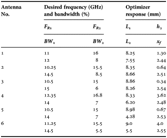
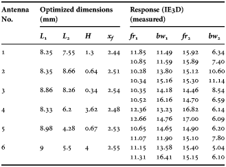
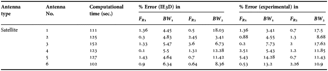
The frequency and bandwidth range used for the training of ANN black-box was 8–18 GHz and 8–18%, respectively. Therefore, the present design process can only be applied for designing dual-broadband antenna in this frequency range. The highest specified bandwidth for the lower and upper bands was restricted to 18 and 8%, respectively, because of the fixed values that have been taken for some of the substrate parameters. Six dual-broadband antennas with specified bandwidths have been designed using the developed modified optimizer. The convergence plot of the optimizer for one of the antenna designs using the modified algorithm is shown in Fig. 7. The optimized design parameters (L 1, L 2, h 2, and x f ) along with other constant values (h 1 = 1.53 mm, ε r1 = ε r3 = 2.2, h 3 = 3.06, ε r2 = 1, tanδ 1 = tanδ 3 = 0.0009, tanδ 2 = 0, t 1 = t 2 = 0.002 mm) were used to simulate the structures using IE3D simulation software. Also, fabrication of the six antennas was done in the laboratory using the optimized parameters. The picture of a typical fabricated prototype is shown in Fig. 8. Figures 9–11 compare the simulated and measured |S 11 | (in dB) for the six experimental prototypes, where a good match between the two can be seen which confirms the validity of the proposed design procedure. The simulated E- and H-plane radiation patterns at 10.35 and 14.46 GHz for one of the antennas (Antenna No. 3) are shown in Fig. 12. These patterns show broadside radiation with little variation in the pattern over the bandwidth. The numerical values of optimizer response, simulation, and experimental results have been listed in Tables 1 and 2.

Fig. 8. Photograph of fabricated antenna.
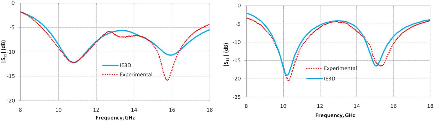
Fig. 9. Reflection coefficient performance plot for the Antenna No. 1 and Antenna No.2.
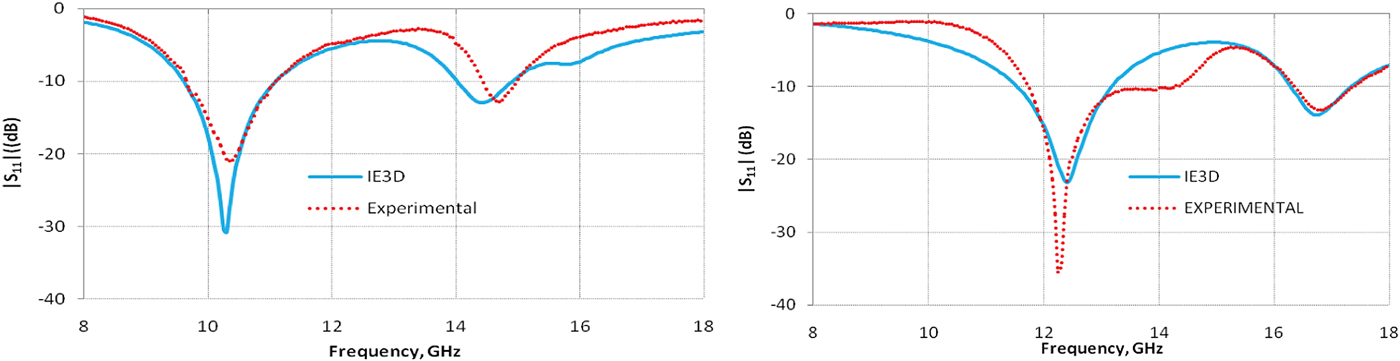
Fig. 10. Reflection coefficient performance plot for the Antenna No. 3 and Antenna No.4.

Fig. 11. Reflection coefficient performance plot for the Antenna No. 5 and Antenna No.6.

Fig. 12. E- and H-field radiation pattern for the Antenna No. 3 at 10.35 and14.46 GHz.
Table 1. Optimizer responses for satellite antenna (X-Ku band).

Table 2. Simulated and experimental response for optimized antennas.

Desired resonance frequencies and bandwidth are compared with simulation and measurement results. Validity of the developed methodology can be confirmed clearly from these data. Finally overall performance of the modified optimizer in terms of computational time and error can be estimated numerically from the Table 3.
Table 3. Performances evaluation of the proposed optimizer.

VI. CONCLUSION
In general, the conventional microstrip patch antenna is a narrow band radiator and a stacked structure is commonly used for bandwidth enhancement. In normal practice, a patch antenna design task is carried out using electromagnetic simulator with repeated simulations till the desired resonant frequency and bandwidth are achieved. In the present work, a systematic design procedure has been proposed for the design of a stacked patch antenna using a trained ANN with a particle swarm optimizer which reduced the computational burden considerably. In order to make the entire design process fast and flexible, fitness function required for modified optimizer has been evaluated using a trained ANN beforehand. This speeds up the design process and the antenna dimensions required for achieving the user-specified resonant frequencies and bandwidth can be easily obtained. The proposed design process has been validated by designing, fabricating, and testing several stacked patch antennas. The prime goal of this work was to develop a designer-friendly CAD tool for the speedy design of the stacked patch antennas for operation in the X-Ku band. Although here we have considered only the resonant frequencies and the bandwidths as the desired goal, the methodology can be further refined to include other desired characteristics like desired E-field radiation pattern, H-field radiation pattern, gain, directivity, and efficiency.
ACKNOWLEDGEMENTS
This work has been supported by the Advanced Microwave Group (I.I.T. Roorkee (U.A.), India). Author is thankful to Prof. S.N. Sinha and Prof. A. Patnaik for this.
 Satish K. Jain received his B.E. degree in Electronics and Instrumentation Engineering from S.A.T.I. Vidisha, (M.P.) India in 1991 and the M.E. degree in Communication Systems from Rani durgawati University Jabalpur (M.P.) India in 1994. He has been awarded Ph.D. in “RF and Microwave” from the Indian Institute of Technology (I.I.T.) Roorkee (U.A.) India in 2013. His research interest includes Microstrip antennas, Application of Soft computing, and Evolutionary optimization techniques in RF and Microwave component design, Smart antennas, Frequency selective surfaces, and Metamaterial in the antenna design etc. Dr. Jain is a life member of many professional organization like IETE, CSI, BES (India), ISOI, ISTE, IEEE, IE (India), and ACEEE (IDEAS).