


Introduction
Modern communication systems require bandpass filters to have good stopband rejection performance to suppress unwanted interfering signals [Reference Cameron1–Reference Cheng, Lin, Lancaster, Song and Fan5]. This performance is especially useful in the high isolation diplexer design [Reference Cheng, Lin, Zhu, Wang and Fan6–Reference Xiao, Zhang and Ma8]. There are two main methods to increase the stopband suppression performance. One is to increase the order of the filter. Nevertheless, a higher order filter leads to a higher insertion loss and a larger circuit size. Another method is to introduce transmission zeros (TZs) at the stopband. A lot of previous works have focused on this topic [Reference Cameron1–Reference Cheng, Lin, Lancaster, Song and Fan5]. For example, the cross-coupling or source-load coupling techniques were widely adopted to improve the stopband selectivity or stopband rejection level [Reference Cameron1, Reference Zhou, Lancaster and Huang2]. Theoretically, with cross-coupling or source-load coupling, an n th-order filter can have a maximum of n TZs. However, with the increment number of TZs, the structure of the filter became more complex. Using mixed electric and magnetic couplings between adjacent and non-adjacent resonators is also a way to generate the TZs. The fabricated fourth-order filter showed two TZs [Reference Venanzoni, Dionigi, Tomassoni and Sorrentino3]. In [Reference Zhang, Long, Zhou, Qiao, Hou and Tian4] and [Reference Cheng, Lin, Lancaster, Song and Fan5], TZs were achieved by introducing extra resonators loaded at the input or output port. But those extra resonators lead to a large circuit size.
The stub-loaded resonator (SLR), which is also known as the dual-mode resonator, was first reported in [Reference Lee, Cho and Yun9]. It has been successfully used in the high selectivity balun filter design [Reference Xu, Wang, Zhu, Huang and Wu10], multiband filter design [Reference Ma, Wei, Hong, Cao, Guo and Jiang11], and tunable filter design [Reference Tang and Hong12]. The traditional SLR is composed of two λ/4 microstrip sections and a center tapped open stub. This kind of SLR can generate two transmission poles (TPs) and one TZ. The open stub controls not only the TZ, but also the bandwidth of the filter. These two parameters are not independent. Different from the previous SLRs, the microstrip sections in our work are shorter than λ/4, and each SLR can generate one TP and one TZ. Similarly, the frequency of the TZ can be easily controlled by the length of the open stub. It indicates that with the properly designed coupling structure, an n th-order filter can have n TZs. In this paper, the coupling structure is realized by the short-circuit stub, which behaves as a K-inverter. The bandwidth of the filter is no longer related to the open stub but the K-inverter values only. Based on the classical K-inverter method [Reference Matthaei, Young and Jones13], a complete design procedure for the proposed filter is described in detail. A microstrip filter is fabricated to verify the theory. The measured results show that the third-order filter has a center frequency of 2.44 GHz with a bandwidth of 0.18 GHz. Three TZs are located at 3.1, 3.9, and 5 GHz, respectively. The stopband rejection is better than 59 dB from 2.93 to 5.01 GHz. Compared with a high selectivity filter, the filter in this paper may suppress the interfering signals at some frequencies further from the passband, which may be used as one channel filter of a high isolation diplexer.
Characteristics of the SLR
Figure 1 shows a typical structure of an SLR which can be equivalent to a λ g/4 type SIR. The resonator has an open stub with a characteristic impedance Z 2 and electrical length θ 2 connected to two symmetrical microstrip sections with a characteristic impedance Z 1 and an electrical length θ 1. The two microstrip sections are shorted to ground. If all resonators are cascaded by the K-inverters at the shorted end, TZs can be created by the open stubs. The frequencies of the fundamental and harmonic TZs can be obtained by
 $$f_{zpn}\, = \,{{(2n-1)\,{90}^\circ \,f_0} / {\theta _2}},$$
where f 0 is the center frequency of the filter, n represents the n th TZ, and n = 1, 2, 3,…. In this paper, we only consider n = 1. According to equation (1), when θ 2 < 90°, the TZ is above the passband.

Fig. 1. Structure of an SLR and a step-impedance resonator (SIR).
The input impedance of the SLR seen from one short end is
 $$Z_{in}\, = \,jZ_1\,\displaystyle{{{\tan} ^2\theta _1-2R_z\tan \theta _1\cot \theta _2} \over {\tan \theta _1-R_z\cot \theta _2 + R_z{\tan} ^2\theta _1\cot \theta _2}},$$
where R z is the impedance ratio which is defined by R z = Z 2/Z 1. The reactance slope of the resonator is defined and derived as
 $$x\, = \,\left. {\displaystyle{{\omega_0} \over 2}\,\displaystyle{{dX(\omega )} \over {d\omega}}} \right \vert _{\omega = \omega _0}\, = \displaystyle{{Z_1} \over 2}\cdot \displaystyle{N \over D},$$
 $$N = 2\theta _1\tan \theta _1\sec ^2\theta _1-2R_z\theta _1\sec ^2\theta _1\cot \theta _2 + 2R_z\theta _2\tan \theta _1\csc ^2\theta _2,$$
 $$D = \tan \theta _1-R_z\cot \theta _2 + R_z\tan ^2\theta _1\cot \theta _2.$$
Let Z in = 0, we can get the resonance condition for the fundamental resonance
 $$2R_z\cos (R_n\theta _1)\cos (R_n\theta _2)-\sin (R_n\theta _1)\sin (R_n\theta _2) = 0,$$
where R n is the frequency ratio of the n th higher order resonant frequency to the fundamental one. Figure 2(a) shows the calculated θ 1 versus θ 2 under different R z. As shown, θ 1 and θ 2 are always smaller than 90°. Note that when R z = 0.5, the SLR behaves as a quarter-wavelength resonator. Figure 2(b) shows the frequency ratios with different electrical length θ 2. The SLR's first spurious frequency is associated with the characteristic impedance ratio R z. To get a good stopband rejection, the first spurious frequency of the resonator should be higher than the TZ's frequency. In the filter design, for a given R z, θ 2 should be chosen to obey this rule.
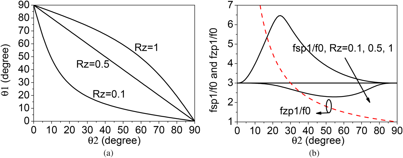
Fig. 2. (a) Calculated electrical length of the microstrip section versus the electrical length of the open stub with different impedance ratios, (b) frequency ratios versus the electrical length of the open stub with different impedance ratios.
Inductive-coupling element
Two microstrip sections with a short-circuit stub in the center can be equivalent to a K-inverter as shown in Fig. 3. The short-circuit stub can be equivalent to an inductor. The inductance can be extracted by a full-wave simulator [Reference Cheng, Lin, Hu, Liu, Song and Fan14]. This circuit is used to realize the inductive-coupling between two adjacent SLRs. It should be mentioned that this inductive-coupling element not only acts as the K-inverter but also is a part of the SLR. By comparing the ABCD matrices of the equivalent circuit and the K-inverter, it can be obtained
 $$\left \vert {\displaystyle{{X_{ij}} \over {\sqrt {Z_{i1}Z_{\,j1}}}}} \right \vert = \displaystyle{{{{K_{ij}} / {\sqrt {Z_{i1}Z_{\,j1}}}}} \over {\sqrt {(1-{(K_{ij}/Z_{i1})}^2)(1-{(K_{ij}/Z_{\,j1})}^2)}}}, $$
 $$\varphi _{ija} = -\displaystyle{1 \over 2}\tan ^{-1}\left( {\displaystyle{{2{{Z_{\,j1}} / {X_{ij}}}} \over {{{Z_{i1}} / {Z_{\,j1}-{{Z_{\,j1}} / {Z_{i1} + {{Z_{i1}Z_{\,j1}} / {X_{ij}^2}}}}}}}}} \right),$$
 $$\varphi _{ijb} = -\displaystyle{1 \over 2}\tan ^{-1}\,\left( {\displaystyle{{2{{Z_{i1}} / {X_{ij}}}} \over {{{Z_{\,j1}} / {Z_{i1}-{{Z_{i1}} / {Z_{\,j1} + {{Z_{i1}Z_{\,j1}} / {X_{ij}^2}}}}}}}}} \right).$$
Fig. 3. Equivalent circuit model of the K-inverter.
With the given values of the K-inverters and the characteristic impedance of the microstrip lines, the inductance values and the electrical lengths of the microstrip lines can be calculated using the above equations.
Synthesis procedure of the filter
Figure 4 shows the equivalent circuit model of the proposed third-order filter. The synthesis procedure is summarized as follows.

Fig. 4. Equivalent circuit model of the proposed filter, (a) with the K-inverters, (b) with the inductors, (c) with the microstrip sections absorbed.
Firstly, the design parameters for the SLRs and the K-inverter values in Fig. 4(a) are calculated according to the filter specification. According to the TZ's frequency, θ i2 can be calculated by (1). Then, according to the required center frequency, θ i1 can be obtained by (4). Then, from (3), we can get each SLR's reactance slope x i. According to the required passband ripple level and the fractional bandwidth, the element values g i are found. Take the reactance slope into the following equations
 $$K_{01} = \sqrt {\displaystyle{{Z_0Z_{11}x_1FBW} \over {g_0g_1}}}, $$
 $$K_{ij} = FBW\sqrt {\displaystyle{{Z_{i1}Z_{\,j1}x_ix_{i + 1}} \over {g_ig_{i + 1}}}}, $$
 $$K_{n,n + 1} = \sqrt {\displaystyle{{Z_{n1}Z_0x_nFBW} \over {g_ng_{n + 1}}}}. $$
we can get the required K-inverter values (j = i + 1).
Then, all K-inverters are transformed into their equivalent circuits, resulting in the equivalent circuit shown in Fig. 4(b). Take K ij into equation (5), we can get the reactance of the inductor X ij, φ ija, and φ ijb. Then, the inductance L ij can be calculated.
The microstrip sections for the inverters are absorbed into the SLRs and the input/output feeding line. The final equivalent circuit in Fig. 4(c) can be obtained.
The proposed filter is designed with a center frequency of 2.45 GHz, and a 3 dB bandwidth of 0.19 GHz. Three TZs are designed to be at 3, 4 and 5 GHz, respectively. A Chebyshev low-pass prototype with 0.01 dB ripple is chosen for this design. The associated element values of the low-pass filter prototype are {g 0, g 1, g 2, g 3, g 4, g 5} = {1, 0.6292, 0.9703, 0.6292, 1}. All the microstrip transmission lines have the same characteristic impedance of 50 Ω. After the above synthesis procedure, all the design parameters are calculated and listed in Table 1.
Table 1. Design parameters for the third-order filter

Fabrication and measurement
A prototype filter with the design specification given at the previous section is fabricated. An F4B substrate with a dielectric constant of 2.55, loss tangent of 0.001, thickness of 0.8 mm, and copper thickness of 0.018 mm is used. Figure 5 shows a photograph of the fabricated filter. The size of the filter is 61.57 mm × 19.1 mm which can be further reduced by folding microstrip lines. The synthesized, simulated, and measured results are shown in Fig. 6. Table 2 compares the simulated and measured results. All the results agree with each other very well. The passband covers the entire 2.4 GHz Wi-Fi band with return loss larger than 20 dB. With the three TZs located at 3.1, 3.9, and 5 GHz, the stopband suppression of the proposed filter is better than 59 dB from 2.93 to 5.01 GHz.
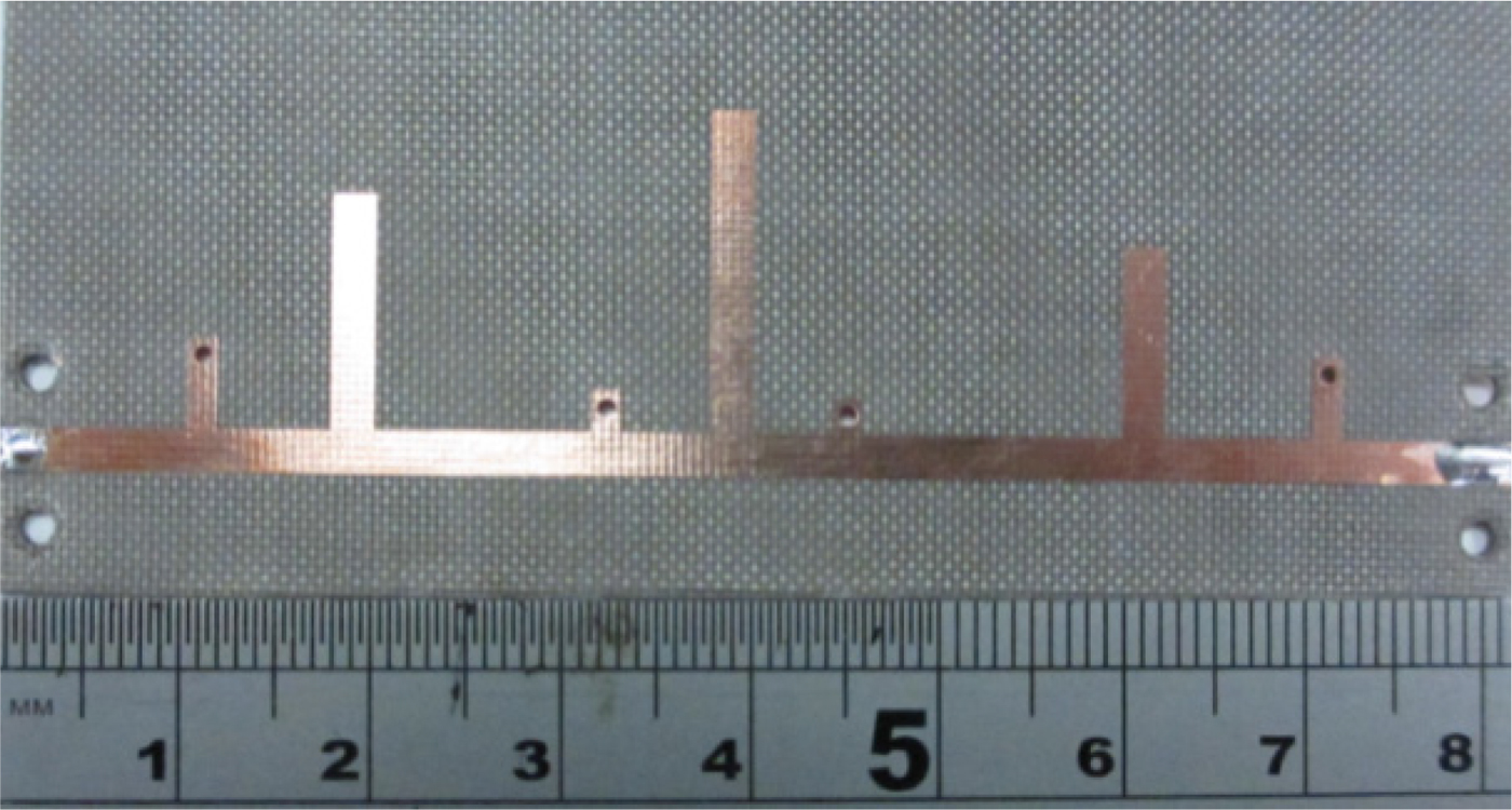
Fig. 5. Photo of the fabricated filter.

Fig. 6. Comparison of S-parameters of the synthesis, electromagnetic simulation, and measurement.
Table 2. Comparison of simulation and measurement

Conclusion
In this paper, a bandpass filter using inductive-coupled SLR is proposed. The characteristics of the SLR and the inductive-coupling structure are studied. The synthesis procedure of the filter is given. The synthesized, simulated, and measured results agree with each other very well. Due to that the SLR can produce TZs, the filter exhibits deep stopband suppression. The filter can be used in the future communication system which needs high-level stopband suppression.
Acknowledgement
The authors would like to thank Dr. Jiafeng Zhou from the University of Liverpool for his valuable suggestions. This work was supported by the National Natural Science Foundation of China under project number 61801317.
 Fei Cheng received the B.S. degree from Xidian University, Xi'an, China, in 2009, and the Ph.D. degree from the University of Electronics Science and Technology of China, Chengdu, China, in 2015. From 2013 to 2015, he was a visiting Ph.D. student at the University of Birmingham, UK. From 2015 to 2017, he was with Chengdu Jiuzou Dfine Technology Co. Ltd. as a microwave engineer. Since July 2017, he joined Sichuan University as an assistant professor. His main research interests are microwave components such as filter, antenna, and rectifier.
 Ping Lu received the B.S. degree in electrical engineering and automation from Southwest Jiaotong University, Chengdu, China, in 2012, and the Ph.D. degree in radio physics with the University of Electronic Science and Technology of China, Chengdu. From 2015 to 2017, she was a Joint Ph.D. Student Scholar at the Laboratoire Ampére, École Centrale de Lyon, INSA de Lyon, Université Claude Bernard de Lyon, Villeurbanne, France. Since July 2018, she joined Sichuan University as an assistant professor. Her current research interests include rectenna, non-diffraction beams, and wireless power transmission.
 Kama Huang received the M.S. and Ph.D. degrees in microwave theory and technology from the University of Electronic Science and Technology of China (UESTC), Chengdu, China, in 1988 and 1991, respectively. He joined the Scientific Research Center “Vidhuk” Ukraine, Kiev, Ukraine, in 1996, the Institute of Biophysics CNR, Genoa, Italy, in 1997; Technical University Vienna, Vienna, Austria, in 1999; and Clemson University, Clemson, SC, USA, in 2001, as a Visiting Scientist. He has been a professor with the Department of Radio and Electronics, Sichuan University, Chengdu, since 1994, where he has also been the Director since 1997. His current research interests include wireless energy transmission, microwave chemistry, and electromagnetic theory.


