Introduction
In modern communication systems, both power dividers and bandpass filters (BPFs) are fundamental elements. Power dividers are widely used to divide/combine signals in various RF/microwave system such as feeding network of antenna array and multichannel circuits. BPFs are extensively employed in the RF front-end due to its ability of selecting desired signal and suppressing unwanted signal.
Wilkinson power divider [Reference Wilkinson1] is first introduced in 1960; it is still the most popular power divider even in modern wireless systems due to its simple layout and perfect isolation between two output ports. Nevertheless, the traditional Wilkinson power divider always suffers from spurious passbands at odd-time harmonics. To improve the out-of-band performance, several techniques such as DGS [Reference Park, Yun and Ahn2, Reference Ting, Tan and Martins3], capacitors [Reference Ting, Tan and Martins3, Reference Zhang, Dai, Kao, Wei, Cai and Xue4], stub-loaded resonators [Reference Nosrati, Faraji and Atlasbaf5, Reference Wu, Chu, Tian and Ouyang6], discriminate coupling [Reference Lin7] and coupled lines [Reference Tang, Lin, Liu and Fan8] have been proposed in the past few decades. These effective measures could also be utilized to design power dividers [Reference Wu, Liu and Li9–Reference Gao, Sun and Xiao26].
Generally, in modern wireless system, power dividers and BPFs are always cascaded to achieve power-splitting and filtering response [Reference Zhu, Amin and Guo:13–Reference Chao and Li15]. However, this approach will result in large circuit area occupation and increase the insertion loss. In order to further reduce the circuit size, one effective way is to integrate the two components into one circuit. Nowadays, some designs with dual function of dividing and filtering have been proposed. In [Reference Wang, Zhang, Liu and Lee16, Reference Chau, Hsu and Tu17], power dividers with wide stopband are realized by replacing the traditional quarter-wavelength transmission line with frequency selectivity structure. However, the rejection level in the stopband and the isolation between the output ports should be improved [Reference Wang, Zhang, Liu and Lee16], and the operating bandwidth is not wide [Reference Chau, Hsu and Tu17]. The resonator-based filtering power dividers with good in-band splitting and harmonic-suppressed performance have been proposed in [Reference Zhao, Gao, Zhang and Xu18, Reference Chen, Huang, Shen and Wu19]. In [Reference Shao, Huang and Pang20–Reference Wang, Zhang and Hu25], filters are used as the impedance transformers to replace the quarter-wavelength transmission line in the traditional Wilkinson/Gysel power divider, and the two ports of the filters are matched to 70.7 Ω rather than 50 Ω. However, the operating bands of these circuits in [Reference Zhao, Gao, Zhang and Xu18–Reference Wang, Zhang and Hu25] are not wide or the out-of-band performance are not good enough. Recently, wideband power dividers have been proposed utilizing different techniques such as stub-loaded ring resonator [Reference Gao, Sun and Xiao26], wideband multilayer microstrip-to-slot transition structures [Reference Xu, Wang, Chen, Zhang and Zheng27, Reference Song and Xue28] and embedded transversal filter sections [Reference Jiao, Wu, Liu, Xue and Ghassemlooy29]. However, the upper stopband is narrow or the rejection level should be improved.
According to the recent progress in filtering power divider above, it can be obtained that wide band filtering power divider has a narrow stopband or low rejection level. Similarly, wide stopband filtering power divider usually has a narrow operating band. Few works with wide working band and broad stopband have been reported. In this study, a wideband filtering power divider with high-frequency selectivity and good out-of-band performance is proposed. Two BPFs with four transmission zeros (TZs) distributed in the two sides of the passband are embedded in the Wilkinson power divider, a resistor is specially arranged between the two BPFs for isolation. Main features of the proposed circuit include: (1) dual functions of power splitting and filtering; (2) wide operating bandwidth; (3) enhanced out-of-band performance with the presence of four TZs; (4) owning wide operating band and wide/deep stopband simultaneously.
The rest of this paper is arranged as follows. “Analysis of the proposed power divider” section employs the even- and odd-mode methods to obtain the design equations. “Design examples and experimental results” section presents the simulated and measured results of a fabricated filtering power divider to validate the proposed concept. Finally, “Conclusion” section draws a brief conclusion.
Analysis of the proposed power divider
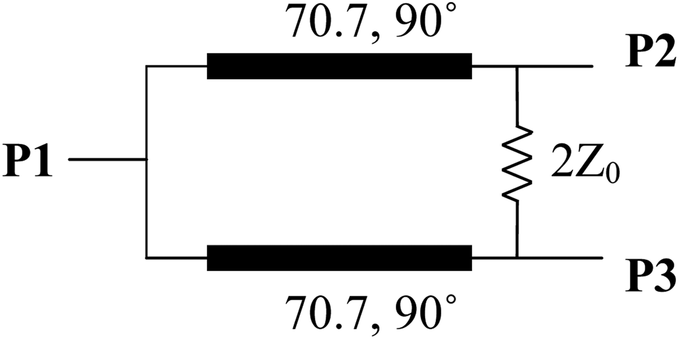
The conventional Wilkinson power divider is shown in Fig. 1. It is composed of two quarter-wavelength (λ g/4) transmission line with characteristic impedance of 70.7 Ω and a lumped isolation resistor of 100 Ω, the termination of three ports is 50 Ω. The layout of the Wilkinson power divider is simple, but it suffers from poor frequency selectivity around the operating band and the fractional bandwidth (FBW) is narrow. The selectivity can be improved by cascading BPF at the input/output port. However, this approach may lead to large circuit size and increase the insertion loss.

Fig. 1. Conventional Wilkinson power divider.
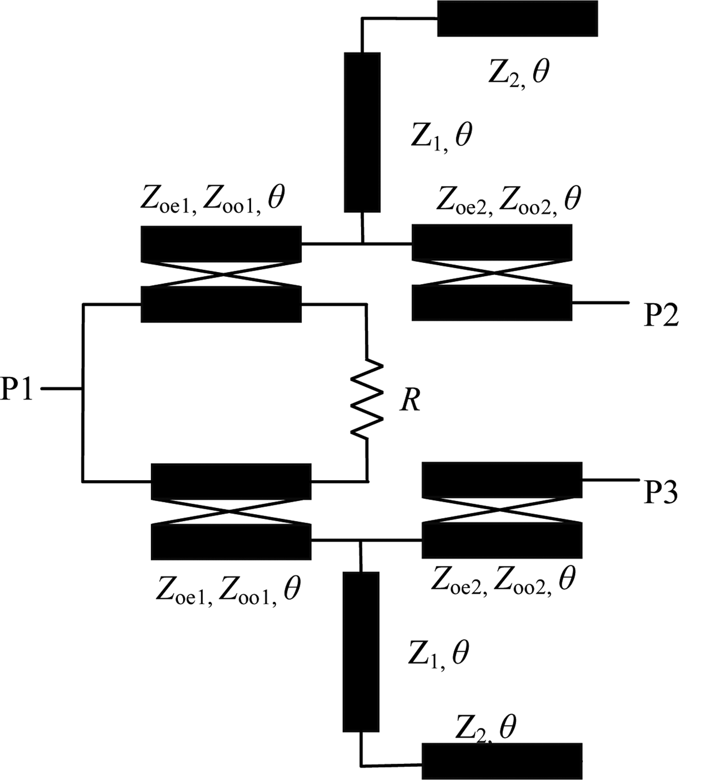
The proposed filter-based power divider is shown in Fig. 2, two BPFs are employed to function as impedance transformer, a resistor is specially arranged for impedance matching and isolation. Z oei and Z ooi (i = 1, 2) are the even- and odd-mode characteristic impedances of the coupled line, respectively. θ is quarter-wavelength at the central operating frequency f 0. Z 1 and Z 2 are the characteristic impedances of the central-loaded stepped-impedance stub.

Fig. 2. Schematic representation of the proposed wideband power divider.
Odd-mode excitation
As the circuit is symmetric, the even- and odd-mode methods can be applied. When the circuit is excited by odd-mode source, the voltage along the symmetrical plane is zero. We can bisect the circuit by grounding the symmetrical plane. Figure 3(a) depicts the equivalent circuit of the proposed power divider under odd-mode excitation.
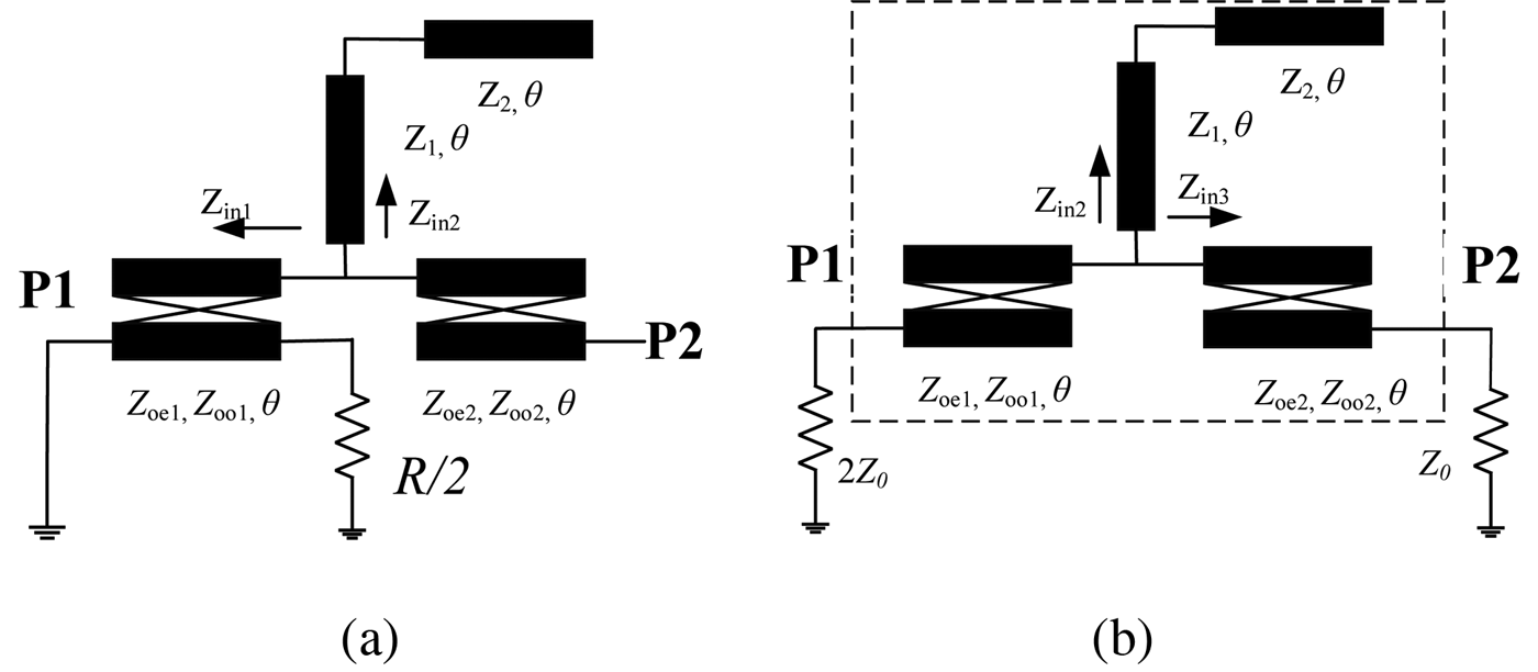
Fig. 3. Equivalent circuit of the proposed power divider under (a) odd-mode excitation and (b) even-mode excitation.
In Fig. 3(a), according to the current and voltage relationships [Reference Hong and Lancaster30], the resistance looking from the middle point into port 1 can be expressed as follows:
 $$\eqalign{ Z_{in1} =\;& Z_{{\rm 11}} - Z_{12}\left( {\displaystyle{{Z_{12}} \over {R/2 + Z_{11}}} + \displaystyle{{Z_{14}(((Z_{14}Z_{12})/(R/2 + Z_{11})) - Z_{13})} \over {Z_{11}(R/2 + Z_{11}) - Z_{14}^2}}} \right) \cr & +\; Z_{{\rm 13}}\displaystyle{{((Z_{14}Z_{12})/(R/2 + Z_{11})) - Z_{13}} \over {Z_{11} - (Z_{14}^2 /(R/2 + Z_{11}))}},} $$
where Z 1i (i = 1, 2, 3, 4) are the elements of the Z-matrix of the first coupled line. The resistance looking from the midpoint to the central-loaded open stub can be expressed as:
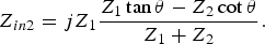 $$Z_{in2} = jZ_1\displaystyle{{Z_1\tan \theta - Z_2\cot \theta} \over {Z_1 + Z_2}}.$$
Assuming perfect impedance matching is achieved at the output port P2, the following equation can be obtained:
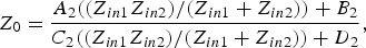 $$Z_0 = \displaystyle{{A_2((Z_{in1}Z_{in2})/(Z_{in1} + Z_{in2})) + B_2} \over {C_2((Z_{in1}Z_{in2})/(Z_{in1} + Z_{in2})) + D_2}},$$
where A 2B 2C 2D 2 are the parameters of the second coupled line. By substituting (1) and (2) into (3) and separating the real and imaginary parts of (3), the following equations can be obtained:
 $$(Z_{oe2} - Z_{oo2})^2 - (Z_{oe2} + Z_{oo2})^2\cos ^2\theta = 4\sin ^2\theta Z_0^2. $$
At the central frequency, (4) can be simplified and is expressed as:
 $$Z_{oe2} - Z_{oo2} = 2Z_0,$$
 $$R = \displaystyle{P \over Q},$$
where
 $$\eqalign{P =\; & 2(Z_{oe1} + Z_{oo1})( - Z_0Z_1^2 (Z_{oe1} + Z_{oo1}) \cr & + Z_0(2Z_2Z_{oe1}Z_{oo1} + Z_1(2Z_{oe1}Z_{oo1} + Z_2(Z_{oe1} + Z_{oo1})))\cot ^2\theta ) \cr & + j2Z_1Z_2Z_{oe1}Z_{oo1}\cot ^3\theta - j2Z_1^2 Z_{oe1}Z_{oo1}\cot \theta,} $$
 $$\eqalign{Q =\; & jZ_0(Z_{oe1} + Z_{oo1})[Z_2(Z_{oe1} + Z_{oo1}) + Z_1(2Z_2 + Z_{oe1} + Z_{oo1})]\cot ^3\theta \cr & - Z_1^2 (Z_{oe1} - Z_{oo1})^2\csc ^2\theta \cr & + jZ_0 \left[ - Z_1(Z_{oe1} - Z_{oo1})^2 - Z_2(Z_{oe1} - Z_{oo1})^2 \right.] \cr & \left.[- Z_1^2 (Z_{oe1} + Z_{oo1}) + Z_1^2 (Z_{oe1} + Z_{oo1})\cos (2\theta )\right]\cot \theta \csc ^2\theta \cr & + Z_1\cot ^2\theta [Z_1(Z_{oe1} + Z_{oo1})^2 + Z_2(Z_{oe1} - Z_{oo1})^2\csc ^2\theta ] \cr &- Z_1Z_2(Z_{oe1} + Z_{oo1})^2\cot ^4\theta .} $$
Even-mode excitation
When the proposed circuit is excited by even-mode excitation, the symmetrical plane is a magnetic wall. There is no current flowing through the isolation resistor, so the resistor can be omitted. The impedance at port 1 is doubled in the bisected circuit; the equivalent circuit under even-mode excitation is shown in Fig. 3(b).
The impedance looking from the midpoint to port 2 is expressed as Z in3; it can be calculated and expressed by the following equation:
 $$Z_{in3} = \displaystyle{{A_2Z_{L3} + B_2} \over {C_2Z_{L3} + D_2}},$$
where
 $$Z_{L3} = Z_0.$$
Similarly, assuming perfect impedance matching is achieved at port 1, we can obtain
 $$2Z_0 = \displaystyle{{A_1((Z_{in2}Z_{in3})/(Z_{in2} + Z_{in3})) + B_1} \over {C_1((Z_{in2}Z_{in3})/(Z_{in2} + Z_{in3})) + D_1}}.$$
By combing (2), (9), and (11), and after some algebraic manipulation, we obtain
 $$(Z_{oe1} - Z_{oo1})^2 - (Z_{oe1} + Z_{oo1})^2\cos ^2\theta = 8\sin ^2\theta Z_0^2. $$
At the central frequency, the following equation can be expressed as:
 $$Z_{oe1} - Z_{oo1} = 2\sqrt 2 Z_0.$$
In summary, design formulas of the proposed power divider can be obtained by equations in (5), (6), and (13).
Bandpass filter
In Fig. 3(b), the circuit in the dash block is a BPF. Its performance has important influence on the filtering response of the whole circuit. So we will discuss it in detail.
Figure 4 shows the schematic of the BPF. Transmission-line theories are applied to analyze the proposed circuit. The ABCD matrix of the filter can be obtained by multiplying the matrices of the coupled lines and open stub, and can be derived by:
 $$M_{\,filter} = M_1 \times M_2 \times M_1,$$
where M i (i = 1, 2) is the matrix of the coupled line and open stub. With the conversation of ABCD matrix to S-parameters, the TZs can be derived by setting S 21 equal to zero, and the TZs can be expressed as:
 $$\eqalign{ f_{z1} &= \displaystyle{{{\rm 2}n\pi + \arccos ((Z_1 - Z_2)/(Z_1 + Z_2))} \over \pi} \cr f_0&= \displaystyle{{{\rm 2}n\pi + \arccos ((k - 1)/(k + 1))} \over \pi} \quad f_0{\kern 1pt} (n = 0,1,2, \ldots ),}$$
 $$ \eqalign{ f_{z2}& = \displaystyle{{{\rm 2}n\pi - \arccos ((Z_1 - Z_2)/(Z_1 + Z_2))} \over \pi} \cr f_0 &= \displaystyle{{{\rm 2}n\pi - \arccos ((k - 1)/(k + 1))} \over \pi} \quad f_0(n = 1,2,3 \ldots ),}$$
 $$f_{{\rm z3}} = 2nf_{0\;}\;\;\;(n = 1,2,3...),$$
where
 $$k = \displaystyle{{Z_1} \over {Z_2}}.$$
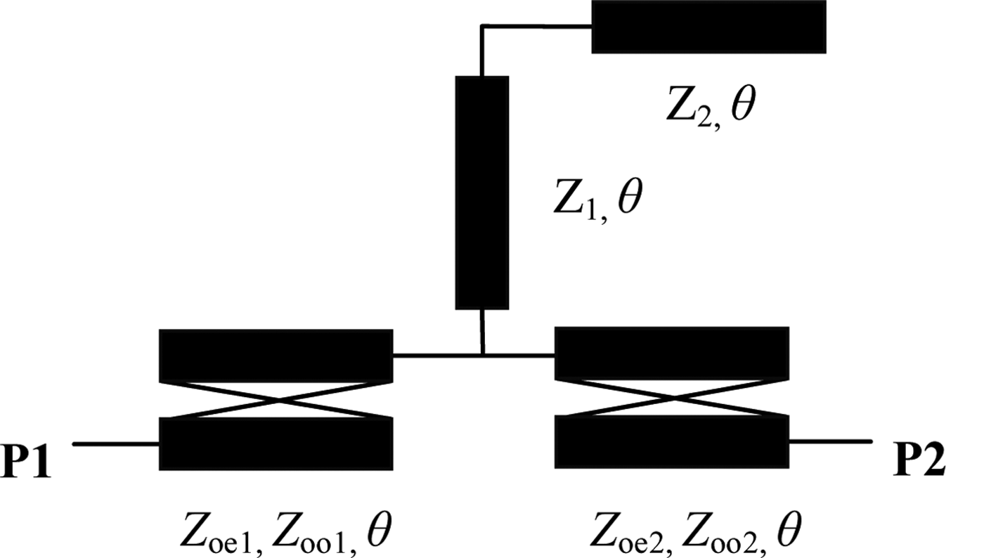
Fig. 4. Schematic representation of the proposed wideband filter.
In equations (15)–(17), it can be found that f z1 and f z2 are only related with the characteristic impedance ratio k, and f z3 is only related with the central frequency. By tuning the value of k, the locations of f z1 and f z2 vary and the frequency selectivity changes. So it is very clear that the performance of the proposed circuit is improved by the generated TZs.
Figure 5 depicts the theoretical response of the proposed BPF calculated by MATLAB under different values of k with Z oei, Z ooi (i = 1, 2) fixed at 163 and 70 Ω, respectively. It is clear that f z1 and f z2 are located near the edges of the passband, which are very beneficial to improve the frequency selectivity. Furthermore, it can be obtained that the locations of f z1 and f z2 vary along with the impedance ratio k. Meanwhile, f z3 is irrelevant with the characteristic impedance of the transmission line; its location is fixed once the central frequency is determined. The trend of the TZs locations varying along with different values of k is in accordance with the equations in (15)–(17), verifying the validity of the analytical analysis above. It also can be found that the bandwidth and the out-of-band rejection level of the proposed BPF change when the value of the impedance ratio k varies. These features can be applied to design filters with controllable operating bandwidth, TZs, and wide stopband by properly choosing the characteristic impedances.
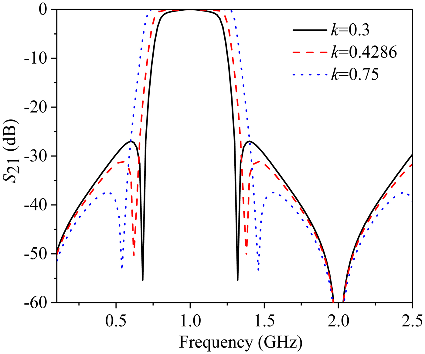
Fig. 5. Calculated results of the proposed BPF under different values of k with Z 0e = 163 Ω, Z 0o = 70 Ω.
Design procedure
Based on our method, we can design a wideband filtering power divider with good out-of-band performance. The design procedures are summarized as follows:
(1) Choosing the characteristic impedances of the coupled lines to fulfill the equations in (5) and (13).
(2) Adjusting the values of Z 1 and Z 2 to meet the required 3 dB bandwidth.
(3) Calculating the value of the resistor according to the equation in (6), once the values of Z 1 and Z 2 are determined.
(4) Optimizing the parameters above to improve the performance of the power divider.
Design examples and experimental results
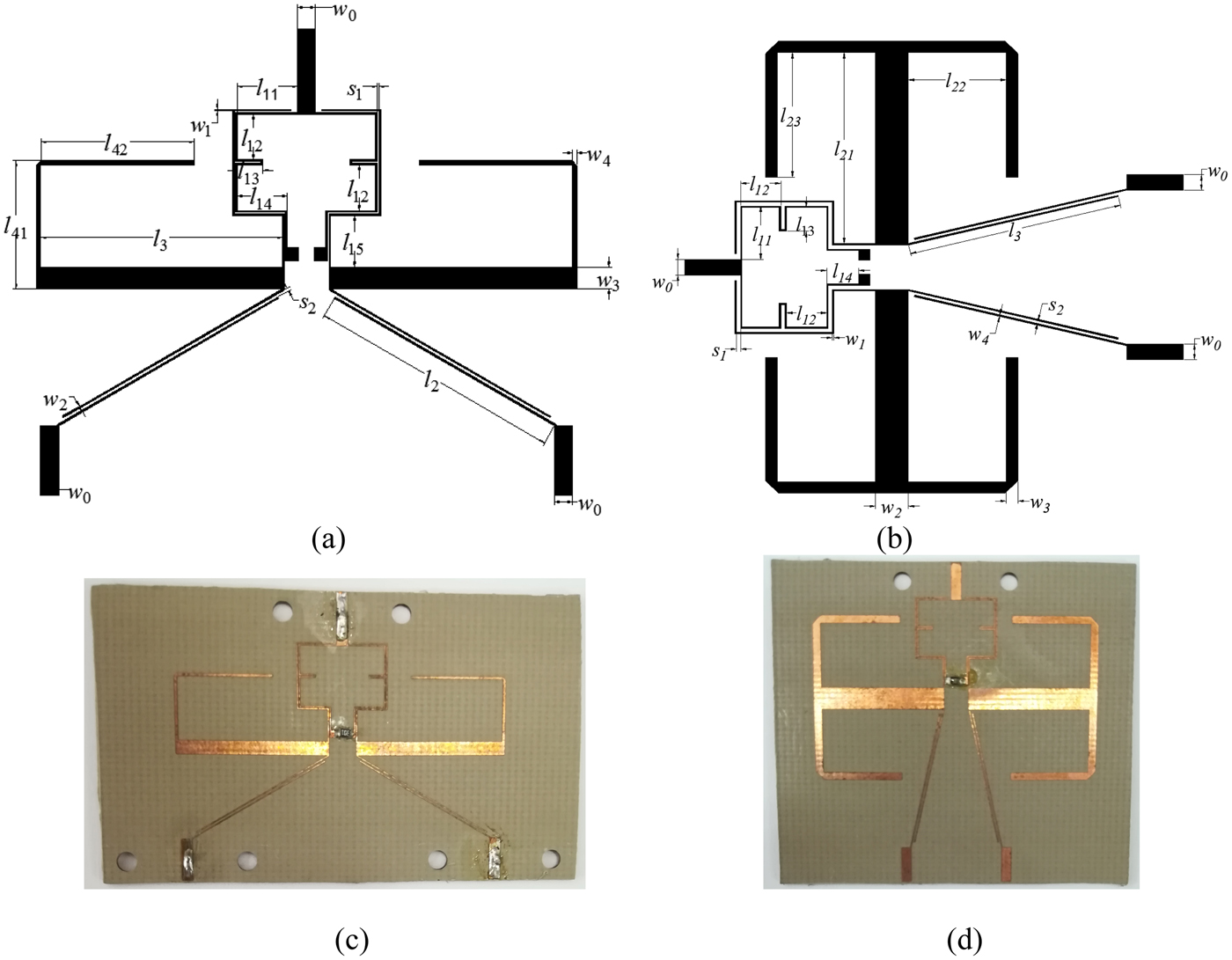
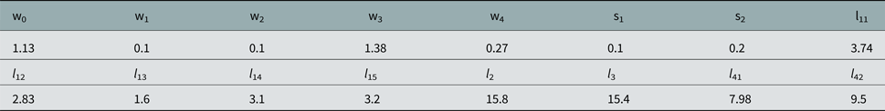
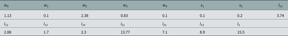
To validate the design concept proposed above, two power dividers PD-A and PD-B with different k are fabricated on a 0.5 mm Taconic RF-35 substrate with ξr = 3.5 and tan δ = 0.0018. The circuits are simulated by a commercial software; HFSS 3D finite-element method is applied to carry out the electromagnetic simulation. As the narrowest gap of the coupled line fabricated is 0.1 mm, the characteristic impedance satisfied with the equation in (15) cannot be implemented on the chosen substrate. Considering the fabrication capacity and performance of the power dividers, the parameters of the proposed circuits adopted are listed in Table 1.
Table 1. Parameters of the proposed two power dividers (unit: Ω)

In Table 1, the theoretical value of the resistor is 338 Ω, but in real implementation, the value of the resistor is selected as 330 Ω. To investigate the impact of resistor tolerance on the circuit behavior, theoretical results of the proposed power dividers with different values of R (338 ± 20 Ω) are displayed in Fig. 6. It is found that the tolerance of the resistor R causes a small performance degradation.

Fig. 6. Theoretical results of the proposed circuits under different values of R. (a) PD-A, (b) PD-B.
The layout and picture of the fabricated two power dividers are shown in Fig. 7, and its detailed dimension parameters are listed in Tables 2 and 3, respectively. The even- and odd-mode phase velocities of the practical microstrip coupled line are different, which will result in unwanted harmonics around 2nf 0 (n = 1, 2, 3…). So part of the coupled line connected with port 1 is meandered to compensate this phenomenon, as shown in Fig. 7. The simulated results of the proposed PD-A with and without meandered structure are compared in Fig. 8. It can be found that the spurious passband around 2f 0 is suppressed in the circuit with meandered structure, whereas the frequency response at other frequencies is almost the same.

Fig. 7. Layout and picture of the fabricated power dividers. (a) Layout of PD-A, (b) layout of PD-B, (c) picture of PD-A, (d) picture of PD-B.
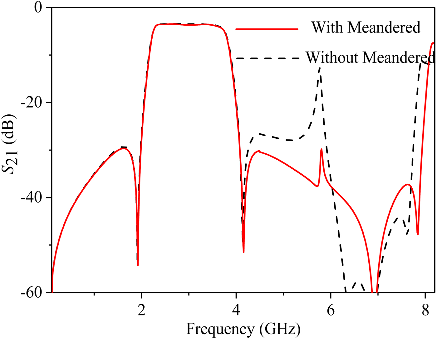
Fig. 8. Simulated results of the proposed circuit with and without the meandered structure.
Table 2. Detailed parameters of the fabricated PD-A (unit: mm)

Table 3. Detailed parameters of the fabricated PD-B (unit: mm)
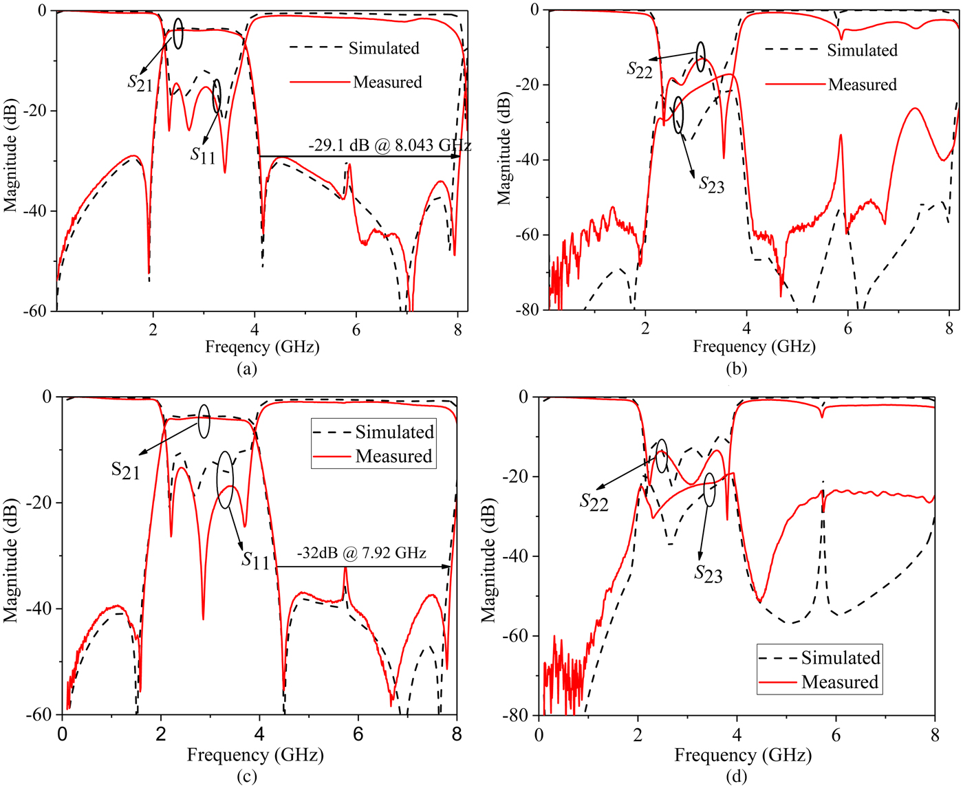
The circuits are measured by an Agilent N5244A network analyzer. Simulated and measured results are depicted in Fig. 9. Good agreement is achieved between the simulated and measured results.

Fig. 9. Measured and simulated results of the fabricated power dividers. (a) S 21 and S 11 of PD-A, (b) S 23 and S 22 of PD-A, (c) S 21 and S 11 of PD-B, (b) S 23 and S 22 of PD-B.
For power divider A, the measured 1 dB passband is from 2.26 to 3.71 GHz, FBW of 48.6%. The insertion loss at the central frequency, i.e. 2.98 GHz, is 3.86 dB. The bandpass bandedges’ skirts of insertion loss are sharpened by two TZs (f z1 and f z2) located at 1.913 and 4.172 GHz. The return loss at the input and output ports in the passband is better than 14.5 and 13.5 dB, respectively. The rejection level is higher than 28.9 dB in the lower stopband, and in the upper stopband, the spurious suppression is larger than 29.1 dB from 4.5 to 8.04 GHz (2.7 f 0). The isolation between the two outputs in the passband is better than 17.2 dB.
For power divider B, the measured 1 dB passband is from 2.05 to 3.89 GHz, with FBW of 62% at the central frequency of 2.97 GHz. Two TZs (f z1 and f z2) near the passband are located at 1.57 and 4.49 GHz. The measured insertion losses of S 21 at the central frequency are 3.72 dB, and both the input and output return losses in passband are better than 13.5 dB. The rejection level in the lower stopband is better than 38.2 dB, and in the upper stopband, the spurious suppression is larger than 32 dB from 4.34 to 7.92 GHz (2.67f 0). The isolation between the two outputs in the passband is better than 19.2 dB.
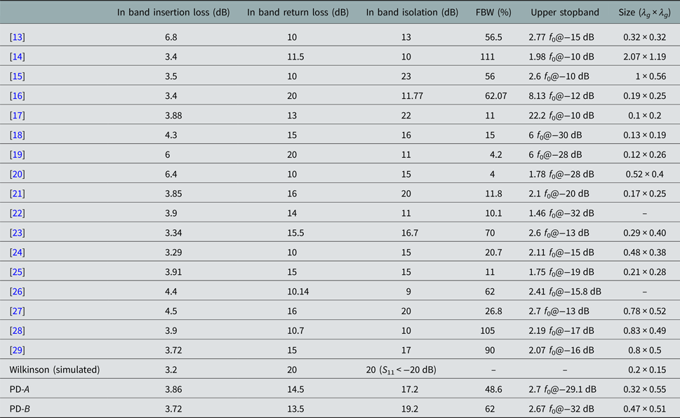
Comparisons between the proposed power dividers, standard Wilkinson power divider (built with the same substrate and operating at the same frequency), and previously reported ones are listed in Table 4. Compared with the standard Wilkinson power divider, the proposed circuits have the advantage of filtering function. The works in [Reference Zhu, Amin and Guo:13–Reference Chao and Li15] are realized by cascading the filtering circuits with the power dividers; compared with these circuits, the proposed circuits have the merits of wider and deeper stopband, and the circuit is are more compact when compared with the works in [Reference Wong and Zhu14, Reference Chao and Li15]. The circuit in [Reference Wang, Zhang, Liu and Lee16] shows wide working band and broad upper stopband. Nevertheless, when considering the rejection level larger than 30 dB, its stopband is relatively narrow; and the isolation between the two output ports is not high. The works in [Reference Chau, Hsu and Tu17–Reference Chen, Huang, Shen and Wu19] show wider stopband than the proposed PDs. However, the operating band of these two works are relatively narrower, and the insertion loss is larger than the proposed circuits. Compared with the works in [Reference Shao, Huang and Pang20–Reference Jiao, Wu, Liu, Xue and Ghassemlooy29], the proposed circuits have merits of wide and deep stopband. In a word, the proposed circuit could provide a wide operating band, wide and deep stopband simultaneously.
Table 4. Comparisons between the fabricated and previously reported filtering power dividers

Conclusion
A filtering power divider with the features of high-frequency selectivity, wide operating band, low insertion loss, good isolation, and wide and deep stopband is presented in this research. Filtering response is realized by two embedded BPFs, which replace the conventional quarter-wavelength transmission line. Besides, a resistor is arranged between the two BPFs to achieve good isolation. By tuning the impedance ratio of the center load open stubs, locations of TZs can be shifted to improve the frequency selectivity. Finally, two prototype power dividers are designed, fabricated, and measured. Good agreement is observed between the simulated and measured results, validating the proposed design concept. Future attention will be paid to suppress more harmonics of the circuit.
Acknowledgement
This work was supported in part by the National Natural Science Foundation of China (No. 61571084), in part by the Program for New Century Excellent Talents in the University (No. NCET-13-0095), in part by the FRF for CU (No. ZYGX2014J016), and in part by the SRF for ROCS, SEM.
 Pengcheng Zhang was born in Sichuan, China, in 1987. He received the B.Sc. degree in electromagnetic and wireless technology from the University of Electronic and Science Technology of China (UESTC), Chengdu, China, in 2011. Now, he is pursuing the Ph. D degree in electromagnetic and microwave technology in UESTC. His interests include antenna design, metamaterial, microwave and millimeter-wave absorber.
 Xian Qi Lin was born in Zhejiang Province, China, on July 9, 1980. He received the B.S. degree in electronic engineering from the University of Electronic Science and Technology of China (UESTC), Chengdu, China, in 2003, and Ph.D. degree in electromagnetic and microwave technology from Southeast University, Nanjing, China, in 2008. He joined the Department of Microwave Engineering at UESTC in August 2008, and has become an Associate Professor and a doctoral supervisor since July 2009 and December 2011, respectively. From September 2011 to September 2012, he was a post-doc researcher in the Department of Electromagnetic Engineering at Royal Institute of Technology (KTH), Stockholm, Sweden. He is currently a Full Professor in UESTC. He has authored over 10 patents, over 40 scientific journal papers, and has presented over 20 conference papers. His research interests include microwave/millimeter-wave circuits, metamaterials, and antennas. Dr. Lin is a member of IEEE and a reviewer of many well-known journals such as IEEE-MTT/AP/MWCL/AWPL, JEMWA/PIER, and EL. He was the recipient of 2011 honorable mention for the national hundred outstanding doctoral dissertations, a 2012 excellent young scholar presented by UESTC, and a 2013 new century excellent talent in the University presented by the Ministry of Education.
 Cong Tang was born in Shangqiu, Henan Province, China. He received the B.S. degree in electronic engineering from the PLA Information Engineering University, Zhengzhou, China in 2010, and is currently working toward the Ph.D degree at the University of Electronic Science and Technology of China (UESTC), Chengdu, China. His research interests include millimeter-wave and microwave devices, circuits, and systems.
 Yuan Jiang (S'12) was born in Jiangsu Province, China. He received the B.S. and M.S. degrees in electronic engineering from the University of Electronic Science and Technology of China, Chengdu, China, in 2010 and 2012, respectively, where he has been working toward the Ph.D. degree since 2012. His research interests include microwave passive components, active components, and antennas, with a particular focus on reconfigurable/tunable technologies.
 Yong Fan was born in 1963. He received the B.E. degree from the Nanjing University of Science and Technology, Nanjing, Jiangsu, China, in 1985, and the M.S. degree from the University of Electronic Science and Technology of China Chengdu, Sichuan China, in 1992. From 1985 to 1989, he was interested in microwave-integrated circuits. Since 1989, he dedicated himself to researching and teaching on subjects of electromagnetic fields and microwave techniques for many years. His main research fields are as follows: electromagnetic theory, millimeter-wave communication, millimeter-wave and terahertz circuits, etc. Besides, he was interested in other subjects including broadband wireless access, automobile anti-collision, intelligent transportation intelligent transportation, etc. He has authored and co-authored over 130 papers.