INTRODUCTION
It has been found for many years that optoelectronic devices such as solar cells, and photo detectors are fabricated by silicon (Schropp & Zeman, Reference Schropp and Zeman1998; Sze & Ng, Reference Sze and Ng2006). Because of wide spread use of such devices, it has always been of interest to improve the efficiency of particularly solar cells by minimizing their surface reflection to optical lights. Silicon solar cells usually reflect part of incident light and absorb another portion and convert it to electricity. So far, different techniques have been developed by researchers to increase the efficiency of solar cells. For example texturization of nano/micro structures at the front surface of device (Younkin et al., Reference Younkin, Carey, Mazur, Levinson and Friend2003; Carey, Reference Carey2004; Crouch et al., Reference Crouch, Carey, Shen, Mazur and Génin2004a; 2004b; Tull et al., Reference Tull, Carey, Mazur, McDonald and Yalisove2006), using antireflection coating (Kang et al., Reference Kang, Ryu, Upadhyaya and Rohatgi2011), and employing diffused structures at the back surface (Zhao et al., Reference Zhao and Wang2006) have been reported.
Texturing is utilized to decrease the reflection losses (by increasing the light trapping) and therefore increase the efficiency in silicon solar cells (Sher et al., Reference Sher, Winkler and Mazur2011; Mahdieh et al., Reference Mahdieh and Sobhani2012). In the texturization method, micro/nano structures such as grooves and pyramids, cone or column structures, and ripple pattern are formed on the surface of silicon (Nakaya et al., Reference Nakaya, Nishida, Takeda, Moriuchi, Tonegawa, Machida and Nunoi1994; Ming et al., Reference Ming, Gang, Jing-Tao and Li2003; Riedel et al., Reference Riedel, Hernandez-Pozos, Palmer and Kolasinski2004; Mansour et al., Reference Mansour, Jamshidi-Ghaleh and Ashkenasi2006; Iyengar et al., Reference Iyengar, Nayak and Gupta2010; Reference Iyengar, Nayak, More, Meyer, Biegalski, Li and Gupta2011) and other materials such as titanium (Trtica et al., Reference Trtica, Batani, Redaelli, Limpouch, Kmetik, Ciganovic, Stasic, Gakovic and Momcilovic2012), steel (Dolgaev et al., Reference Dolgaev, Fernández-Pradas, Morenza, Serra and Shafeev2006), and silver (Latif et al., Reference Latif, Anwar, Aleem, Rafique and Khaleeq-Ur-Rahman2009). In principle, the protruding structures can re-reflect and scatter light back onto the surface. Therefore, the incident light can effectively be trapped between structures where multiple reflections enhance the coupling into the material. In this process, once the incident light gets inside these protruded structures, multiple internal reflections can guide the light into the bulk. On the other hand, refraction at the surface of these structures also leads to transmission of light at oblique angles, which effectively increases the optical path length, and enhances the absorption (Brown & Arnold, Reference Brown, Arnold and Sugioka2010; Sher et al., Reference Sher, Winkler and Mazur2011; Mahdieh et al., Reference Mahdieh and Sobhani2012).
Surface texturing of silicon solar cells can be performed by different means such as mechanical technique (Nakaya et al., Reference Nakaya, Nishida, Takeda, Moriuchi, Tonegawa, Machida and Nunoi1994; Fathe et al., Reference Fath, Marckmann, Bucher and Willeke1995), alkaline chemical etching (Finne et al., Reference Finne and Klein1967; Szlufcik et al., Reference Szlufcik, Leuven, Sivoththaman, Nlis, Mertens and Van Overstraeten1997; Singh et al., Reference Singh, Kumar, Lal, Singh and Das2001; Panek et al., Reference Panek, Lipiński and Dutkiewicz2005), pulsed laser deposition (Wang et al., Reference Wang, Xu, Zhou, Chu and Fu2007 and the references in there), and laser texturing (Dobrzański et al., Reference Dobrzański, Drygała, Panek, Lipiński and Zięba2007; Liu et al., Reference Liu, Zhu, Liu and Zhao2008; Lugomer et al., Reference Lugomer, Maksimović, Karacs and Peto2011;) from which alkaline chemical etching has been historically the main technique.
The study of utilizing laser beam in producing nano structured silicon surface has been mostly focused on direct interaction of laser beam with target surface. However, there are some reports on the deposition of nano particles produced by pulsed laser ablation on the surface of target. For example, Wang et al. (Reference Wang, Xu, Zhou, Chu and Fu2007) produced the silicon nano particles on the silicon surface by using nanosecond laser ablation and deposition technique in high-purity Ar gas. They also studied the influence of pulse repetition rate on the average size of silicon nano particles. In this technique, it is believed that the ablated particles from the silicon target gradually release their kinetic energy by collisions with ambient atoms. In this process, in an appropriate temperature, the condensation among silicon particles and growth of silicon nano particles take place and finally the formed nano particles are transported to the substrate by a diffusion process (Wang et al., Reference Wang, Xu, Zhou, Chu and Fu2007; Fu et al., Reference Fu, Wang, Chu, Zhou, Yu, Han and Peng2005). As Wang et al. (Reference Wang, Xu, Zhou, Chu and Fu2007) discussed, both the nanosecond (Fu et al., Reference Fu, Wang, Chu, Zhou, Yu, Han and Peng2005) and femtosecond (Eliezer et al., Reference Eliezer, Eliaz, Grossman, Fisher, Gouzman, Henis, Pecker, Horovitz, Fraenkel, Maman, Ezersky and Eliezer2005) lasers can be used in preparing nano particles by pulsed laser ablation. They showed that in compare with nanosecond laser, the use of femtosecond laser for the synthesis of nano particles is attractive for several reasons. A typical reason is the study of the hydrodynamics and thermodynamics of the plasma expansion and nano particle formation without any external disturbances during the laser interaction time. In fact, the femtosecond pulse ends before the expansion starts, and thus the femtosecond pulse does not interact with the ejected material.
In laser texturing by direct interaction of laser beam with silicon surface, there are some advantages that are unique, although other methods such as mechanical technique and alkaline chemical etching are recommended for being economic in mass production. For example, texturing of mono-crystalline silicon can be performed by etching in alkaline solutions. However, this technique is an inefficient method for multi-crystalline silicon because of the presence of random crystallographic grain orientations and high selectivity of etching along specific directions (Nijs et al., Reference Nijs, Szlufcik, Poortmans, Sivoththaman and Mertens2001; Panek et al., Reference Panek, Lipiński and Dutkiewicz2005; Dobrzański et al., Reference Dobrzański and Drygała2008). In general, laser texturing is a contactless treatment technique and, independent of crystal grain orientation; it offers localized texturization with a large degree of control over the shape and size of the structures that are formed on the surface (Dobrzański et al., Reference Dobrzański and Drygała2008; Brown & Arnold, Reference Brown, Arnold and Sugioka2010).
Various micro/nano structures can be accurately produced by controlling laser texturing parameters such as spatial and temporal profile, wavelength, texturing environment, and target characteristics (Huang et al., Reference Huang, Carey, Liu, Guo, Mazur and Campbell2006; Reinhardt et al., Reference Reinhardt, Passinger, Zorba, Chichkov and Fotakis2007; Serpengüzel et al., Reference Serpengüzel, Kurt, Inanç, Cary and Mazur2008; Trtica et al., Reference Trtica, Radak, Gakovic, Milovanovic, Batani and Desai2009; Menéndez-Manjón et al., Reference Menéndez-Manjón, Barcikowski, Shafeev, Mazhukin and Chichkov2010; Kolacek et al., Reference Kolacek, Straus, Schmidt, Frolov, Prukner, Shukurov, Holy, Sobota and Fort2012). Laser texturing under different experimental conditions affects laser target interaction and consequently surface topography and its chemical properties. Over the past few decades, several groups have investigated the topography of laser textured silicon surface irradiated by nanosecond laser pulses in vacuum, atmosphere air, or other ambient gases (Lowndes et al., Reference Lowndes, Fowlkes and Pedraza2000; Pedraza et al., Reference Pedraza, Fowlkes and Guan2003; Crouch et al., Reference Crouch, Carey, Warrender, Aziz, Mazur and Génin2004; Jiménez-Jarquín et al., Reference Jiménez-Jarquín, Fernández-Guasti, Haro-Poniatowski and Hernández-Pozos2005; Lugomer et al., Reference Lugomer, Maksimović, Karacs and Peto2011). For example, Jiménez-Jarquín et al. (Reference Jiménez-Jarquín, Fernández-Guasti, Haro-Poniatowski and Hernández-Pozos2005) studied morphological changes induced on the silicon surface irradiated by nanosecond Nd:YAG laser pulses (λ = 1064 nm and 355 nm) under oxygen atmosphere. Early stages of growth of silicon micro-columns and micro-cones formed by pulsed excimer laser irradiation of silicon in air and SF6 were also studied by Lowndes et al. (Reference Lowndes, Fowlkes and Pedraza2000). Very recently, we reported the results of structure and optical reflectivity of polished silicon irradiated by nanosecond Nd:YAG laser beam (λ = 532 nm) in ambient air (Mahdieh et al., Reference Mahdieh and Sobhani2012). In our experimental conditions, nano structure clusters were formed on the surface of silicon after laser irradiation.
Laser silicon texturing can also be performed in ambient liquids such as water. For example, Shen et al. (Reference Shen, Crouch, Carey and Mazur2004) fabricated sub-micrometer silicon spikes by irradiating silicon surface with femtosecond laser pulses in water. Also, structure formation on the silicon surface irradiated with picosecond laser pulses in air, SF6, and water was reported by Chen et al. (Reference Chen and Vertes2006). However, to our knowledge silicon texturing with nanosecond laser beam in distilled water has not been reported. Moreover, there is no report to compare sub-micro/nano structure formation on the polished silicon surface irradiated by nanosecond laser pulses in ambient air and distilled water.
In this paper, we study sub-micro/nano structure of polished silicon irradiated by nanosecond Nd:YAG laser pulses (λ = 532 nm) in distilled water. In order to estimate the sub-micro/nano clusters height, optical reflectivity of the silicon surface was monitored during the irradiation. A He:Ne laser beam was used to measure the reflectivity of silicon surface before and after irradiation. It will be explained in following sections that the optical reflectivity data gives information on the clusters height. The irradiated silicon surface was investigated by scanning electron microscope. By using an image processing technique the scanning electron microscopy (SEM) images were analyzed from which surface density and diameter distribution of clusters were statistically estimated. Moreover, we compare the results of this investigation with those which were obtained for ambient air as interacting medium.
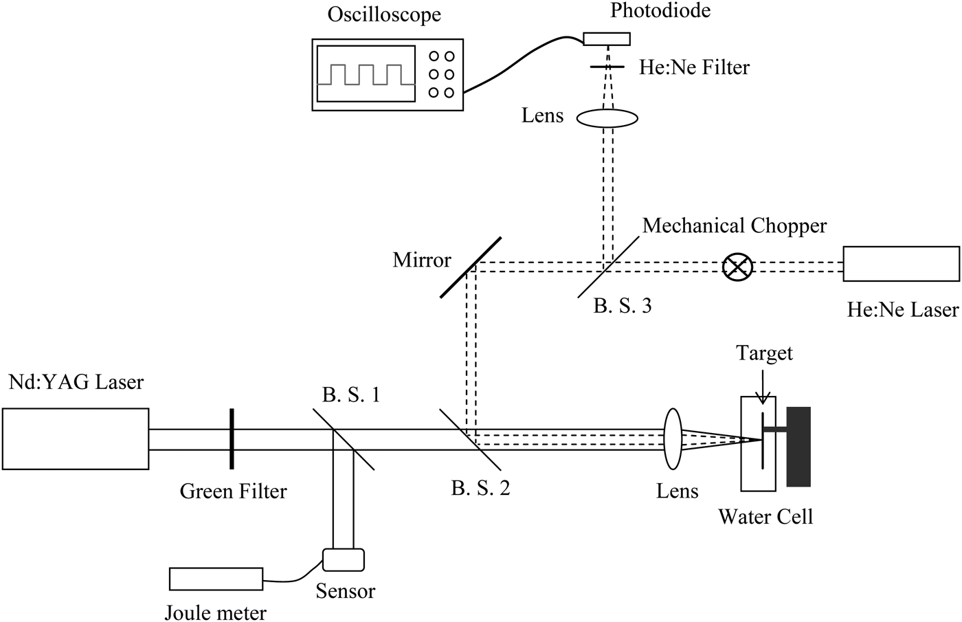
EXPERIMENT AND ANALYSIS TECHNIQUE
Polished side of P-type [100] silicon wafer was textured by Nd:YAG laser irradiation. The Nd:YAG laser (NL303HT, Exspla) was operated at wavelength λ = 532 nm (second harmonic of Nd:YAG laser), and pulse repetition rate of 10 Hz. Laser pulse duration was about 9 ns and irradiation was performed in ambient air and distilled water. Figure 1 shows a schematic setup for the experiment. As the figure shows, a small portion of the laser beam energy was reflected by a beam splitter and measured by Joule meter (Coherent EPM 1000). The transmitted beam was focused on the silicon surface to provide moderate laser fluence for surface texturing. Silicon was irradiated at normal to its surface. A green interference filter blocked the first harmonic of Nd:YAG laser and provided the laser beam with only λ = 532 nm. The target was placed in a small cell. The cell was constructed by using optical windows for better optical performance. It must be noted that for the target irradiation in distilled water, the cell was filled with distilled water. The distilled water in the cell was changed after each stage of irradiation to keep the ambient conditions constant. Enough space between two adjacent irradiated regions was provided by moving the target to a fresh area after each irradiation stage.

Fig. 1. Schematic of experiment setup.
A continuous wave He:Ne laser at wavelength λ = 632 nm was also used to measure the reflectivity of the silicon surface before and after Nd:YAG laser irradiation. A mechanical chopper was used to modulate the He-Ne laser beam. The He:Ne laser beam reflected from the silicon surface was detected by a photodiode and monitored by a digital oscilloscope. A He:Ne filter was placed close to the photodiode in order to block the environmental lights.
Silicon was irradiated with 1000, 2000, 5000, 10000, 15000, 20000, 25000, and 30000 laser pulses. Laser fluences ranging from 0.8 J/cm2 to 1.2 J/cm2, and 6.2 J/cm2 to 8.3 J/cm2 were provided on the surface of silicon immersed in distilled water and air ambient, respectively. It must be noted that these ranges of pulse number and laser fluence for any interaction ambient were used because in the lower limit of the above ranges, the micro/nano structure formation on the silicon surface could be initiated while the upper limit prevents the damage of the silicon surface.
SEM was used to inspect the irradiated regions and characterize the morphology of the surface. Basically, top view SEM image of irradiated silicon gives information on the effective diameter and surface density of clusters. The surface cluster density is referred to the number of clusters per unit area of the target. The SEM images were analyzed by image processing technique from which effective diameter distribution and surface density of clusters were statistically estimated.
RESULTS AND DISCUSSION
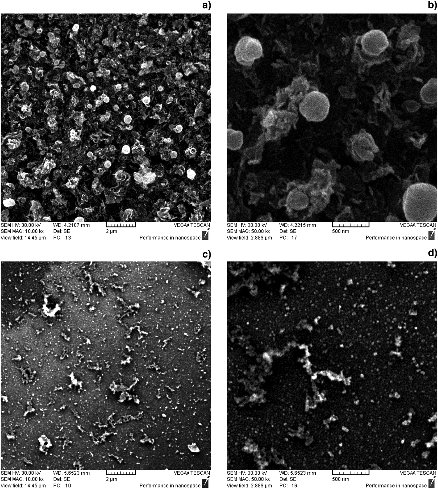
Figure 2 shows typical top view (Fig. 2a) and tilted view (Fig. 2b) SEM images of silicon surface before and after Nd:YAG laser irradiation in ambient distilled water. In Figure 2a, the silicon was irradiated with different pulse numbers (ranging from 5000 to 30000) at a fixed laser fluence of 1 J/cm2. In order to have a rough estimation of surface morphology, Figure 2b is presented. Figure 2b shows the silicon surface that is viewed at an angle of 40° with respect to the surface normal. In Figure 2b, the target was irradiated with 5000 laser pulses at fluence of 1.2 J/cm2. The SEM images show that sub-micron conical clusters with spherical caps are formed on the silicon surface after laser irradiation in ambient distilled water. It can be seen from these images that the height of clusters is at the order of 1µm and their diameter is typically few 100 nm.
Fig. 2. (Color online) The SEM images of polished silicon irradiated in ambient distilled water (a) Top view images of the target which was irradiated with 5000, 15000, 20000, 25000, 30000 pulses at laser fluence of 1 J/cm2 together with an image of non-irradiated target and (b) tilted view of the target irradiated with 5000 pulses at laser fluence of 1.2 J/cm2.
Figure 3 shows other SEM images (with higher magnification) of silicon irradiated in ambient air and distilled water. The irradiation was performed with 15000 pulses at laser fluence of 1 J/cm2 in distilled water (Figs. 3a, 3b), and 10000 pulses at laser fluence of 7.3 J/cm2 in ambient air (Figs. 3c, 3d). Also, the SEM images of silicon surface irradiated with 0 (non-irradiated), 1000, 2000, 5000, 10000, 15000, 20000, 25000, and 30000 laser pulses in ambient air have been shown in our previous work (Mahdieh et al., Reference Mahdieh and Sobhani2012). The laser fluence delivered on the target was about 7.8 J/cm2. According to these figures and Figure 2, nano clusters are formed on the silicon surface after laser irradiation in ambient air while sub-micron clusters are formed under irradiation in ambient distilled water. It must be noted that the cluster formation in ambient air and distilled water was achieved under different conditions of laser parameters (number of pulses and laser fluence) so that the surface of silicon was remained without any damage. In fact, the formed clusters on the silicon surface under irradiation with moderate laser parameters for cluster formation and not in similar conditions of laser parameters in ambient air and distilled water were investigated and compared.
Fig. 3. Top view SEM images of irradiated silicon in distilled water (a, b) and air (c, d) ambient. Laser irradiation was performed with 15000 pulses at laser fluence of 1 J/cm2 (a, b), and 10000 pulses at laser fluence of 7.3 J/cm2 (c, d).
Our observations limited to SEM show that sub-micron/nano clusters are formed on the surface of silicon after laser irradiation. The produced clusters are a group of smaller clusters and more information including the composition of clusters needs some other investigations such as the Raman and X-ray diffraction spectroscopy. It must also be noted that the surface of formed clusters in ambient air and distilled water are covered by silicon dioxide because the laser irradiation was performed in an oxygen rich ambient (Shen et al., Reference Shen, Crouch, Carey and Mazur2004; Pedraza et al., Reference Pedraza, Fowlkes, Jesse, Mao and Lowndes2000).
Clusters formation and their growth process are closely involved to hydrodynamic instabilities and light trapping effect (Brown & Arnold, Reference Brown, Arnold and Sugioka2010; Bäuerle, Reference Bäuerle2011). Laser pulses interacting silicon surface results in plasma formation, surface melting, and material ablation. In fact within the initial phase of irradiation, hydrodynamic motions in laser molten surface and vapor/plasma plume and also their mutual interactions results in the development of instabilities. Hydrodynamic motions can be related to the lateral expansion of the vapor/plasma plume (Bäuerle, Reference Bäuerle2011), the motion of the liquid layer due to the recoil pressure in laser ablation (Kazakevich et al., Reference Kazakevich, Simakin and Shafeev2006), the gas jet in liquid phase explosion (Bäuerle, Reference Bäuerle2011), and/or surface tension effects (Shen et al., Reference Shen, Crouch, Carey, Younkin and Mazur2003). On the other hand, laser pulse duration is short enough and therefore high melting and cooling rate, along with hydrodynamic instabilities, leads to roughness formation on the silicon surface. Additional laser pulses are trapped through multiple reflections in deep regions on the surface and material ablation occurs significantly from these regions. Material ablation and re-deposition result in clusters growth and consequently sub-micron/nano clusters formation on the irradiated regions.
Top view SEM images were analyzed from which the surface cluster density and effective diameter distribution of clusters were estimated. As an example, Figure 4a shows typical top view SEM image of irradiated silicon and Figure 4b shows diagram of surface cluster density versus cluster effective diameter. In this particular figure, the silicon was irradiated with 2000 laser pulses at laser fluence of 8.3 J/cm2 in ambient air. Also, the surface cluster density was estimated in an area of 100 µm2 of the target. This area was used in processing of all images.
Fig. 4. (Color online) Typical top view SEM image of irradiated silicon (a) and diagram of surface cluster density versus cluster effective diameter (b). Silicon was irradiated with 2000 nanosecond laser pulses at laser fluence of 8.3J/cm2 in ambient air.
The effective diameter data shows that the number of formed sub-micron clusters (with diameter 100–500 nm) and nano clusters (with diameter <100 nm) is more significant on the silicon surface after laser irradiation in distilled water and air ambient respectively. This can be also seen in Figures 2 and 3. Therefore, the clusters with these effective diameters ranges were considered in our analysis.
Optical reflectivity of irradiated silicon was also measured by using a He-Ne laser beam operating at wavelength of λ = 632 nm. As explained in the references of Mahdieh et al. (Reference Mahdieh and Sobhani2012), the reflectivity data gives information on micro/nano clusters height. The reflectivity of polished silicon before irradiation was typically about 34%.
The surface density of sub-micron/nano clusters and optical reflectivity of the irradiated silicon were studied in terms of number of laser pulses. Figure 5 shows typical diagrams of surface cluster density and optical reflectivity versus number of laser pulses. In this figure, the irradiation was performed in distilled water (Figs. 5a, 5b) and air (Figs. 5c, 5d) ambient at laser fluences of 1 J/cm2, 1.2 J/cm2, 7.3 J/cm2, and 8.3 J/cm2, respectively. According to these figures, both surface cluster density and optical reflectivity strongly depend on number of laser pulses. From this figure it can be seen that the surface cluster density increases with number of laser pulses and reaches to a maximum value and then decreases gradually or remains almost constant with additional laser pulses. This trend can be also seen in Figure 2a. In fact, most of the irradiated regions are affected slightly by initial laser pulses. However, the surface roughness increases with higher number of pulses. In such condition, the hydrodynamic instabilities are gradually developed on the irradiated region with increasing number of laser pulses. Consequently, the sub-micron/nano cluster morphology is formed more significantly on this region for higher number of pulses and the surface density of clusters increases to a maximum value. On the other hand, further increasing the number of pulses leads to combination of clusters that consequently results in creation of higher size clusters. Therefore, the surface cluster density decreases due to formation of such larger size clusters. Our experiments show that when the number of pulses increases, the chance for creation of larger cluster is higher in distilled water. Such results could be due to higher cooling rate of water with respect to air during and shortly after the irradiation. In fact, distilled water in contact with silicon promotes better energy dissipation from the silicon surface to the distilled water because distilled water has a higher thermal conductivity than air (Yonekubo et al., Reference Yonekubo, Katayama and Sawada2005) (thermal conductivity of water and atmospheric air at 25°C are 0.58 W/m.K and 0.024 W/m.K, respectively). Therefore, the clusters formed in distilled water grow more significantly than in air.
Fig. 5. (Color online) Surface cluster density and optical reflectivity of He:Ne probe beam versus laser pulse numbers. Silicon was irradiated in distilled water (a, b) and air (c, d) ambient at laser fluences of 1 J/cm2 (a), 1.2 J/cm2 (b), 7.3 J/cm2 (c), and 8.3 J/cm2 (d).
Moreover, this figure shows that the optical reflectivity of silicon reduces with number of laser pulses. In fact, multiple reflections by the sides of clusters result in the decrease in optical reflectivity. From this figure it can be concluded that the optical reflectivity of silicon surface is influenced by surface cluster density and clusters height. While the surface cluster density rises to a maximum value, the decrease in optical reflectivity is due to increasing the number of clusters and also clusters height. The surface cluster density decreases with higher number of pulses. However, the surface cluster density may also remain constant at higher number pulses in some laser fluences. Therefore, the decrease in reflectivity with higher pulse numbers can be due to the clusters height increase. In fact, the incident He:Ne beam hitting the higher clusters height has more chance of multiple reflections and as a result further reduction of surface reflection.
The dependence of surface cluster density and optical reflectivity of silicon surface on number of laser pulses was studied at four different laser fluences delivered on the target. The related diagrams are shown in Figure 6. In this figure, the silicon was irradiated at laser fluences of 0.8 J/cm2, 1 J/cm2, 1.1 J/cm2, and 1.2 J/cm2 in distilled water (Figs. 6a, 6b) and laser fluences of 6.2 J/cm2, 7.3 J/cm2, 7.8 J/cm2, and 8.3 J/cm2 in ambient air (Fig. 6c, 6d). As these figures show, the dependence of surface cluster density and optical reflectivity on number of pulses at four laser fluences is similar to those of Figure 5. From this figure it can also be seen that the optical reflectivity of silicon can be reduced to about 7% after irradiation in ambient distilled water while it is reduced to about 23% after irradiation in ambient air. As discussed above, the formed clusters in distilled water grow more significantly than in air. Therefore, formation of higher clusters height in water, results in increase of multiple reflections of the probe beam and consequently further reduction of reflectivity at the silicon surface.
Fig. 6. (Color online) The dependence of surface cluster density and optical reflectivity of silicon surface on number of laser pulses at different laser fluences. Silicon was irradiated at laser fluences of 0.8J/cm2, 1J/cm2, 1.1J/cm2, and 1.2J/cm2 in ambient distilled water (a, b) and laser fluences of 6.2J/cm2, 7.3J/cm2, 7.8J/cm2, and 8.3J/cm2 in ambient air (c, d).
CONCLUSION
Polished side of silicon surface was irradiated by nanosecond laser pulses in ambient air and distilled water. From the results it can be concluded that under the conditions of the experiment, nano structure and sub-micron structure clusters are formed on the silicon surface after irradiation in ambient air and distilled water respectively. The surface cluster density and optical reflectivity of silicon were studied in terms of laser pulse numbers and laser fluence delivered on the target. From the results we concluded that the surface cluster density, optical reflectivity and as a result clusters height are significantly influenced by laser pulse numbers. Moreover, the decrease in optical reflectivity of silicon surface irradiated in distilled water was more significant than in air.