I. INTRODUCTION
WiMAX is a wireless communication standard created by the companies Intel and Alvarion in 2002 and approved by the IEEE under the name IEEE-802.16 which allows data transmission using multiple broadband frequency ranges. The aim of WiMAX is to provide high-speed data rates and internet access in a coverage range of several kilometers in radius. The WiMAX Forum has published three licensed spectrum profiles: the low band 2.3–2.69 GHz, the middle band 3.2–3.8 GHz, and the upper band 5.2–5.8 GHz [Reference Andrews, Ghosh and Muhamed1].
In this paper, a microstrip patch-type high-gain WiMAX antenna with a parasitic radiator and a raised ground plane is presented. High-gain microstrip patch antennas have been investigated before. Effect of a dielectric superstrate layer for high-gain microstrip patch antennas was investigated in [Reference Choi, Cho, Pyo and Choi2]. It was shown in [Reference Choi, Cho, Pyo and Choi2] that the gain of a single patch antenna was enhanced by about 4 dB at 12 GHz. Parasitic elements were employed in the design of a patch antenna to achieve wide bandwidth [Reference Wi, Lee and Yook3]. The presented antenna was inspired by Yildirim and Cetiner [Reference Yildirim and Cetiner4]. It is mentioned in [Reference Yildirim and Cetiner4] that the gain of a conventional microstrip patch antenna can be increased by about 3 dB by placing a rectangular loop shaped parasitic radiator which is placed at a specific distance away from the patch antenna surface. Another gain enhancement technique was proposed in [Reference Jirasakulporn, Chaimool and Akkaraekthalin5] by placing a square aperture superstrate above a patch antenna and a gain improvement of 5.35 dB was achieved. A multilayer parasitic radiator technique was described in [Reference Abdullah, Ali, Ismail, Omar and Dzulkefli6] to enhance the gain of a patch antenna operating at 5.8 GHz WiMAX band. A 3.55 GHz WiMAX patch antenna design has been reported in [Reference Alami, Bennani, Bekkali and Benbassou7]. This design uses an RT/duroid substrate having a loss tangent of 0.001 and has no parasitic radiator. The antenna was fed by a coaxial cable and only simulations have been presented.
The presented antenna has a parasitic patch and a raised ground plane to achieve high-gain operation. The antenna has been analyzed, designed, and fabricated for 3.4–3.6 GHz WiMAX applications. The microstrip patch antenna alone provides a realized gain of about 3.6 dBi at 3.5 GHz. Gain increase is maximum when a parasitic radiator is placed above the surface of the patch antenna at a distance of about 15 mm. For this case, the antenna gain increases from about 3.6 dBi to about 7.4 dBi which is an improvement of 3.8 dB. A raised ground plane further increases the gain by about 1.5 dB. Hence, the total gain improvement is about 5.3 dB.
II. ANTENNA DESIGN
A microstrip patch antenna has three important design parameters. These are the frequency of operation (f 0), relative dielectric constant of the substrate (ε r), and the height of the dielectric substrate (h). The resonant frequency of the antenna is selected as 3.5 GHz. The dielectric material selected for this work is FR4 which has a relative dielectric constant of 4.4. Height of the dielectric substrate is selected as 1.59 mm which is one of the standard substrate thicknesses available in the industry. Patch antenna dimensions can be calculated using the mathematical analysis outlined in [Reference Balanis8, Reference Pozar9]. Based on this analysis, the width of the patch and the effective dielectric constant of the substrate are found as
 $$W=\displaystyle{1 \over {2{f_0}\sqrt {{\mu _0}{\varepsilon _0}} }}\sqrt {\displaystyle{2 \over {{\varepsilon _r}+1}}} = 26.07\; {\rm mm}\comma$$
 $${\varepsilon _{reff}}=\displaystyle{{{\varepsilon _r}+1} \over 2}+\displaystyle{{{\varepsilon _r} - 1} \over 2}{\left[{1 + 12 \displaystyle{h \over W}} \right]^{ - {1 \over 2}}} = 4.$$
The resonant length determines the resonant frequency and is about λ/2 for a rectangular patch excited in its fundamental mode, where λ = c/f 0 = 0.0857 m. The patch is, in fact, electrically a bit larger than its physical dimensions due to fringing fields. The deviation between electrical and physical size is mainly dependent on the circuit board thickness and dielectric constant. A better approximation for the resonant length is
 $${L_{eff}} = \displaystyle{c \over {2{f_0}\sqrt {{\varepsilon _{reff}}} }} = \displaystyle{1 \over 2}\displaystyle{\lambda \over {\sqrt {{\varepsilon _{reff}}} }}=21.53\; {\rm mm}.$$
This formula includes a first-order correction for the edge extension due to fringing fields. For the delta length
 $$\Delta L=0.412h\; \displaystyle{{\left({{\varepsilon _{reff}}+0.3} \right)\left({\lpar W/h\rpar +0.264} \right)} \over {\left({{\varepsilon _{reff}} - 0.258} \right)\left({\lpar W/h\rpar +0.8} \right)}}=0.7\, \; {\rm \mu m} .$$
For the actual length
 $$L={L_{eff}} - 2\Delta \, L=20.11{\rm \; mm} .$$
In summary, the width and the length of the patch are found to be 26.07 and 20.11 mm, respectively, using the mathematical analysis outlined in [Reference Balanis8, Reference Pozar9]. The ground plane dimensions are selected as 100 × 100 mm2. The antenna has been simulated on a 1.59 mm thick FR4 substrate whose relative permittivity is 4.4 and loss tangent is 0.02. There is a 50-Ω microstrip line connecting the patch antenna to the feeding port. The length of this line is l t = 42 mm and its width is w t = 2.8 mm. Having these dimensions, the patch antenna resonates at 3.5 GHz. However, the S11 of the antenna is about −6 dB at the resonant frequency.
Instead of a rectangular patch, design of a square patch has been aimed to reduce the footprint of the antenna. The dimensions of the nearly square patch have been selected as W = 22 mm and L = 19.5 mm at 3.5 GHz. The area of the rectangular patch is the 26.07 × 20.11 = 524.27 mm2 while the area of the nearly square patch is 22 × 19.5 = 429 mm2. So the patch size can be reduced by about 18% if it is made nearly square. The S11 of this nearly square patch is still poor and about −5.5 dB at 3.5 GHz, which implies that the antenna is not well-matched. In order to match the antenna impedance to 50 Ω, a matching circuit is needed. This circuit has been designed using a λ/4 transformer section. The width and the length of this transformer section have been found as w q = 0.6 mm and l q = 12.6 mm, respectively. The antenna dimensions have been slightly changed to achieve the best matching response at 3.5 GHz. After some optimization, the final antenna dimensions are selected as w = 19.6 mm and L = 19.4 mm. The antenna impedance cannot be obtained directly from the simulations. This is because there is a 50-Ω line connecting the antenna to the driving (feeding) port and only the input impedance seen through the driving port can be obtained directly from the simulations. When matching the antenna to the 50-Ω driving port, antenna impedance information is needed at 3.5 GHz. This information has been obtained by subtracting the effect of the transmission line from the driving port impedance using a Smith chart, and is used in the design of the quarter wave transformer section that matches the antenna to the 50-Ω line.
The presented antenna has been designed through extensive three-dimensional electromagnetic simulations using Ansoft HFSS [10] and SEMCAD [11]. Figure 1 shows the top view of the antenna geometry.

Fig. 1. Geometry of the patch antenna with quarter wave long transformer section (W = 19.6, L = 19.4, w t = 2.8, l t = 29.4, w q = 0.6, and l q = 12.6). All dimensions are in millimeters.
Figure 2 shows the simulated and measured S11 of the antenna shown in Fig. 1. Antenna S11 measurements have been performed at TÜBİTAK BİLGEM Electromagnetic and Antenna Systems Division using an Anritsu MS2037C/2 Vector Network Analyzer (VNA). It can be seen from Fig. 2 that S11 measurement and simulation are in excellent agreement. Through the paper, parameter S11 has been used to address how well the antenna is matched to the 50-Ω port. Voltage standing wave ratio (VSWR) could also be used instead of S11, since S11 and VSWR are interchangeable quantities. An S11 value that is lower than −10 dB corresponds to a point within the VSWR circle of 2:1 on the Smith chart. The goal of the matching is to be within the VSWR circle of 2:1 for the desired bandwidth, although being closer to the center of the Smith chart is highly desirable. S11 value of −10 dB is widely used in industry as the border value to describe the quality of the matching. Figure 2 can also be interpreted in this manner.
Fig. 2. Measured and simulated S11 of the patch antenna.
A) The patch antenna on 100 × 100 mm2 ground plane with the parasitic patch
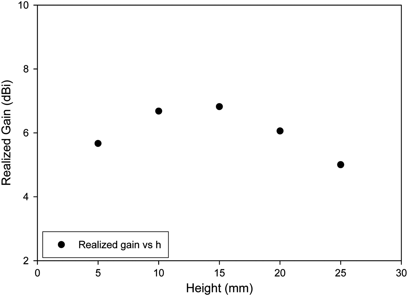
A parasitic patch has been used to increase the realized gain. Through the paper, the term “realized gain” is used over “directivity” since the realized gain is basically the directivity multiplied by the antenna efficiency. Any dielectric, conductor, and mismatch losses contribute to the efficiency of an antenna. For this reason, realized gain has more physical insight than directivity and it is widely used in industry. For the initial design, the size of the parasitic patch has been selected as 23.6 × 23.4 mm2. The distance “h” between the main patch and the parasitic patch is varied with 5 mm intervals. Figure 3 shows that high frequency structural simulator (HFSS) simulated maximum realized gain of the antenna with the parasitic patch increases for certain values of h, when h is varied from 5 to 25 mm with 5 mm steps. The gain improvement is a maximum for h = 15 mm and the realized gain is 6.81 dBi for this case. This can be explained as follows. The main patch and the parasitic patch form an antenna array. When the distance between the two patches is about 15 mm, the radiated fields are constructive and the realized gain increases in the direction of the 0° elevation angle. Away from this distance, the radiated fields are becoming less constructive and the gain decreases. Figure 4 shows the variation of S11 with the frequency when h is varied from 5 to 25 mm with 5-mm steps.
Fig. 3. Realized gain values for different heights of the parasitic patch.
Fig. 4. S11 of the patch antenna for different values of h.
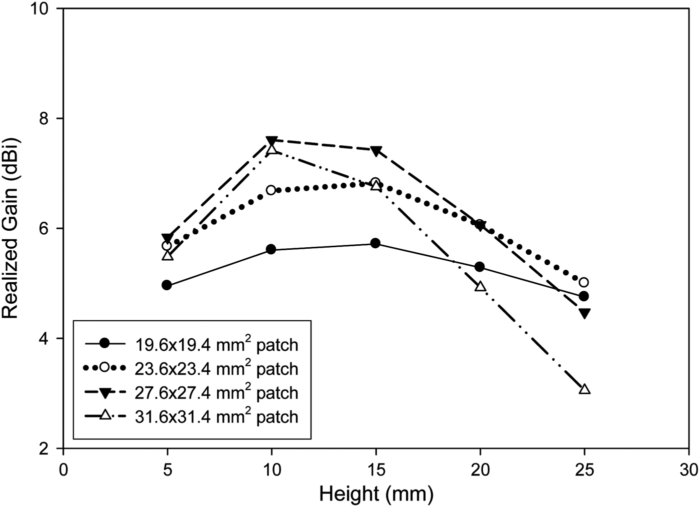
The effect of the size of the parasitic patch on the realized gain has also been studied and the results are shown in Fig. 5. When the parasitic patch size is 23.6 × 23.4 mm2 (this is the reference parasitic patch), the realized gain is 6.81 dBi. When the reference patch size is increased 4 mm in x and y directions (the 27.6 × 27.4 mm2 parasitic patch), the realized gain becomes about 7.43 dBi. When the reference patch size is increased 8 mm in x and y directions (the 31.6 × 31.4 mm2 parasitic patch), a realized gain of 6.75 dBi is obtained. If the size of the reference patch is decreased by 4 mm in x and y directions (the 19.6 × 19.4 mm2 parasitic patch), the realized gain becomes about 5.72 dBi. It can be seen that the maximum realized gain is achieved when the patch size is 27.6 × 27.4 mm2.
Fig. 5. Comparison of realized gains for different sizes of the parasitic patch.
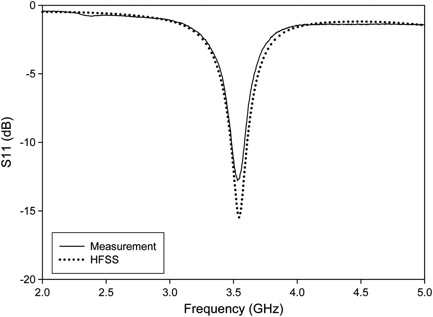
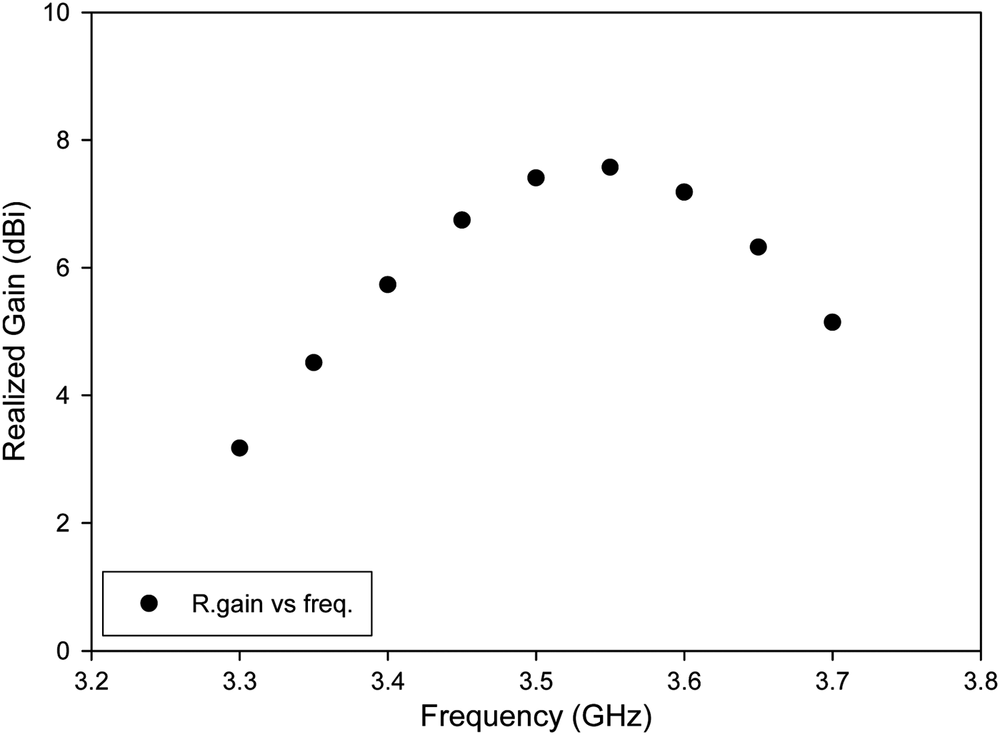
Figure 6 shows S11 measurement and HFSS simulation of the patch antenna for h = 15 mm when the parasitic patch size is 27.6 × 27.4 mm2. It can be seen that the agreement between measurement and HFSS simulation is excellent. Figure 7 shows realized gain as a function of the frequency when the parasitic patch is 15 mm above the main patch and when the size of the parasitic patch is 27.6 × 27.4 mm2. It can be seen from Fig. 7 that frequency-dependent realized gain is maximum at about 3.55 GHz. The gain at 3.5 GHz is approximately 7.4 dBi. Photographs of the fabricated patch antenna with the parasitic patch are shown in Fig. 8. A foam-type material whose relative permittivity is very close to that of air has been placed between the patch antenna and the parasitic radiator as mechanical support. A clear tape, which has no effect on the radiation pattern, is used to keep the foam and the parasitic patch in place.
Fig. 6. S11 of the patch antenna for h = 15 mm and 27.6 × 27.4 mm2 parasitic patch.
Fig. 7. Simulated realized gain as a function of the frequency when the parasitic patch is 15 mm above the main patch and the parasitic patch size is 27.6 × 27.4 mm2.
Fig. 8. Photographs of the fabricated patch antenna with the parasitic patch; (a) top view and (b) side view.
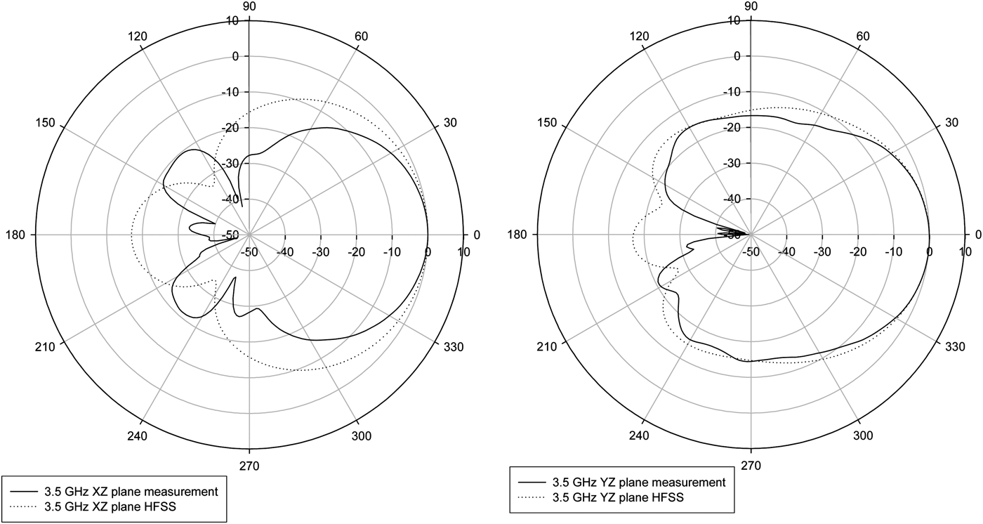
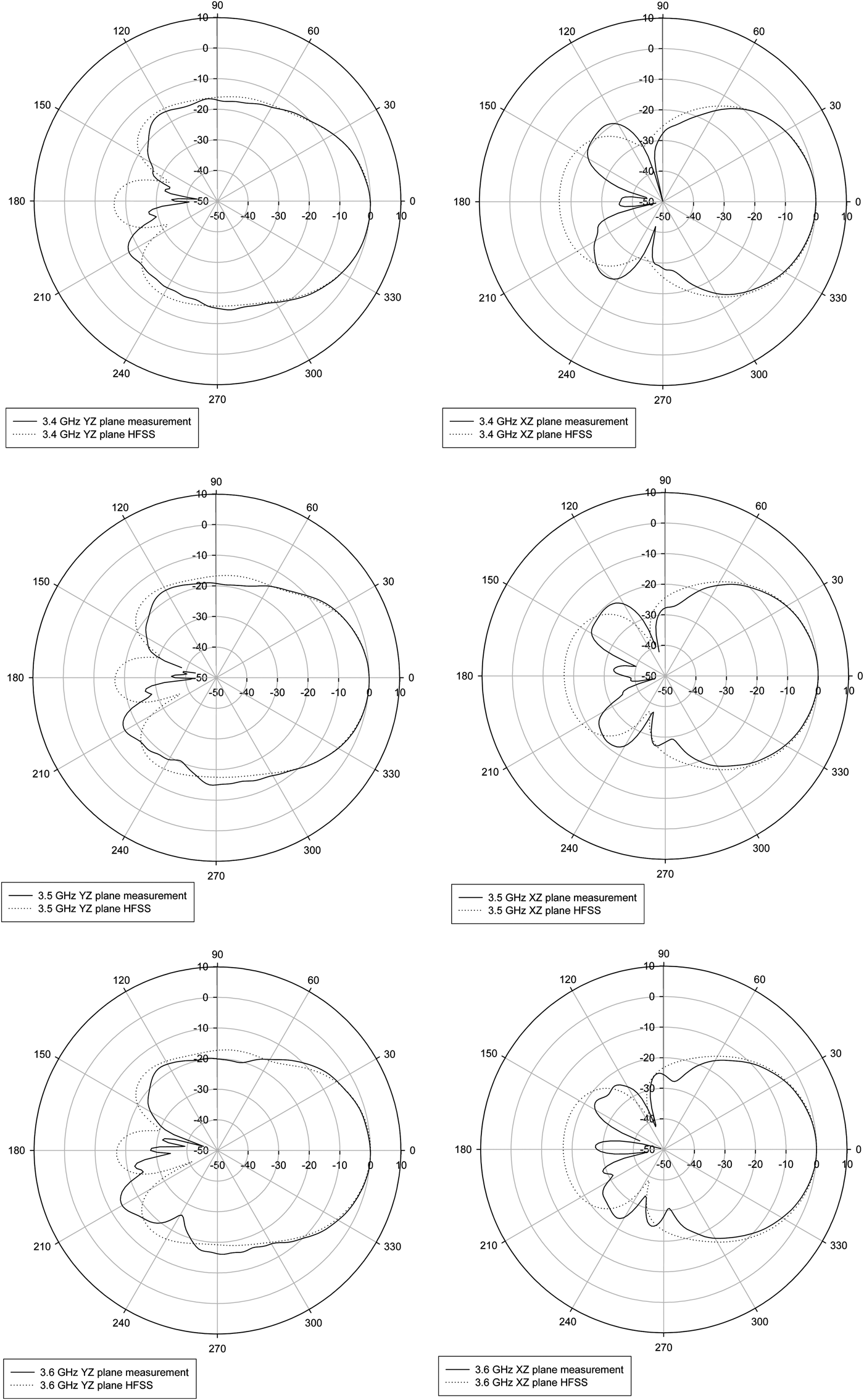
After fixing the distance of the parasitic patch at h = 15 mm for the 100 × 100 mm2 ground plane, the radiation patterns of the antenna at 3.5 GHz are taken in yz, xz, and xy planes. The coordinate system for the radiation patterns is shown in Fig. 1. Figure 9 shows the normalized radiation patterns of the patch antenna at 3.5 GHz for h = 15 mm and 27.6 × 27.4 mm2 parasitic patch size. It can be seen from Fig. 9 that measurement and HFSS simulations are in excellent agreement, the antenna has a peak gain at 3.5 GHz when the elevation angle is zero degrees, and there is not much radiation behind the ground plane.
Fig. 9. Radiation patterns of the patch antenna at 3.5 GHz, for h = 15 mm and when the parasitic patch size is 27.6 × 27.4 mm2.
B) The patch antenna with side walls (right and left)
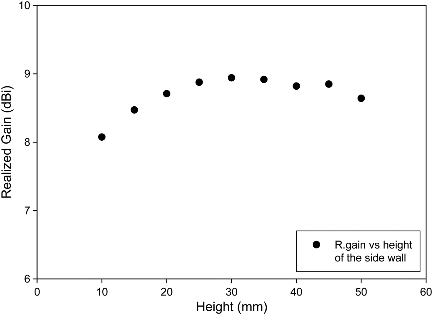
As a next step, two metallic side walls have been added to form a raised ground plane, and the effect of these walls on the S11 and the realized gain have been investigated. When the height of the side walls “d” is varied from 10 to 50 mm with 5 mm steps, the HFSS simulated realized gain varies as shown in Fig. 10. The maximum realized gain is about 9 dBi when d is 30 mm. S11 of this antenna is shown in Fig. 11. It can be seen that the antenna is well matched at 3.5 GHz in the presence of these side walls except there is a slight shift in frequency.
Fig. 10. Realized gain of the patch antenna when the height of the side walls (d) is varied.
Fig. 11. The antenna with left and right side walls, and upper dielectric layer.
C) The patch antenna with two side walls and an upper dielectric layer
In the last section the effect of the right and left side walls and an upper dielectric layer on the antenna radiation pattern have been examined. For this purpose, an upper dielectric layer has been placed as shown in Fig. 11.
This layer has been placed to protect the patch antenna and the parasitic radiator. The dimensions of the upper dielectric layer are 102 × 100 mm2 and made of FR4-type easily available material. The thickness of the FR4 upper layer is 1 mm.
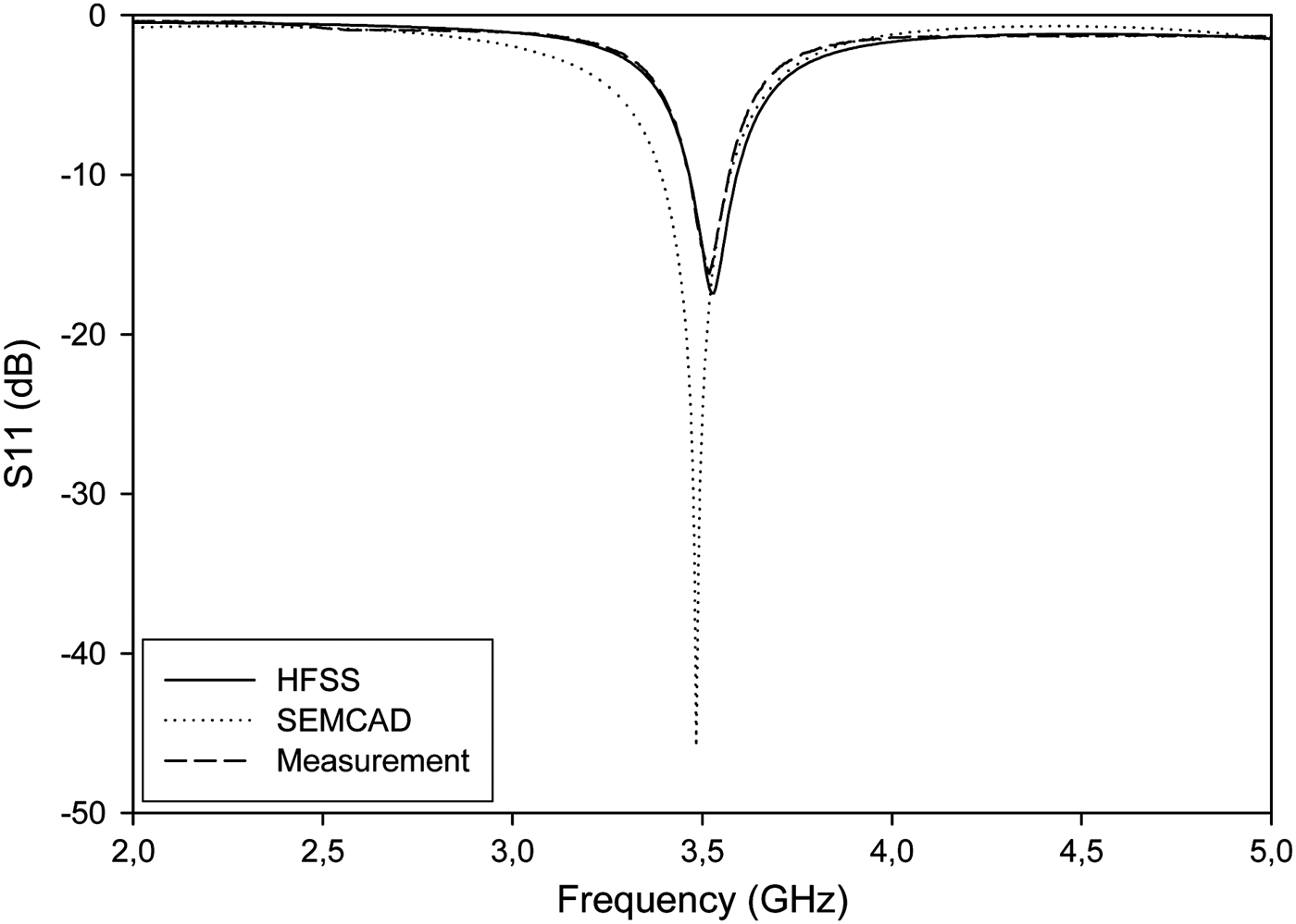
Simulated and measured S11 of the patch antenna with two side walls and an upper FR4 layer is shown in Fig. 12. The resonance frequency shifts up slightly by about 25 MHz from 3.5 to 3.525 GHz in the presence of the side walls and the upper FR4 layer. However, the antenna is still well matched at 3.5 GHz since S11 at 3.5 GHz is about −14 dB. It can be seen from Fig. 12 that S11 measurement and HFSS simulation are in excellent agreement. SEMCAD simulation shows the resonance frequency about 3.48 GHz. The slight discrepancy in simulated resonance frequencies can be due to differences in finite-difference and finite-element techniques which are employed in SEMCAD and HFSS, respectively. Antenna S11 measurements have been performed at Tübitak BİLGEM Electromagnetic and Antenna Systems Division using an Anritsu MS2037C/2 VNA.
Fig. 12. S11 of the patch antenna with two side walls and an upper FR4 layer.
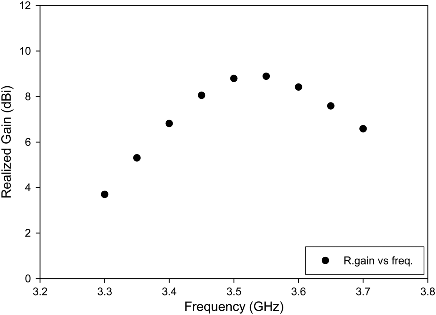
As seen in Fig. 13, the realized gain simulations for the two side walls and upper dielectric layer give the best result at 3.5 GHz. At this frequency the value of the realized gain is approximately 8.9 dBi.
Fig. 13. Realized gain versus frequency.
It can be seen from Fig. 14 that measured and HFSS simulated normalized radiation patterns are in excellent agreement. There is not much radiation behind the ground plane. Beamwidth for 3.5 GHz is about 51° in xz plane and about 47° in yz plane. Finally, the patch antenna with a parasitic patch at h = 15 mm and a parasitic patch size of 27.6 × 27.4 mm2 are selected for fabrication. Also radio-frequency (RF) ground dimensions are selected 100 × 100 mm2. S11 measurements of various designs have been added in this paper. The side-lobe levels and beamwidth information are given in Table 1. For the antenna shown in Fig. 11, surface current distributions are shown in Fig. 15 for 3.4, 3.5, and 3.6 GHz.
Fig. 14. Radiation patterns in yz and xz planes at 3.4, 3.5, and 3.6 GHz.
Fig. 15. Current distributions of the enhanced gain patch antenna at (a) 3.4 GHz, (b) 3.5 GHz, and (c) 3.6 GHz.
Table 1. Side-lobe levels and beamwidths.

III. CONCLUSION
A new and simple technique of improving the gain of a microstrip patch-type WiMAX antenna operating at 3.5 GHz using a nearly square-shaped parasitic radiator and a raised ground plane is presented in this paper. To increase the antenna gain, a parasitic radiator is placed on top of the patch antenna. The patch antenna has been built on low cost and easily available 1.6 mm thick FR4-type substrate with a relative permittivity of 4.4 and a loss tangent of 0.02. Moreover, 100 × 100 and 80 × 80 mm2 RF ground planes have been examined for this process. It was observed that the gain increase is maximum when the distance between the parasitic patch and the main patch is about 15 mm for a 100 × 100 mm2 RF ground plane, and when the parasitic patch has a size of 27.6 × 27.4 mm2. A gain improvement of about 3 dB has been obtained for this case. Additional gain improvement in the order of 1–2 dB has been achieved by adding left and right metallic side walls that are shorted to RF ground. The effect of the different heights of the two side walls on the antenna performance has been examined. The best result has been obtained at 30 mm. The behind wall has not been placed because of an undesirable effect on the radiation pattern of the antenna. Finally, an FR4 layer has been placed on top to protect the patch antenna and the parasitic radiator from impacts. The thickness of the FR4 upper dielectric layer is 1 mm. With this technique, the gain of a conventional microstrip patch antenna can be increased from 3.6 to 8.9 dBi corresponding to 5.3 dB enhancement in gain without the need of an RF amplifier.
The impedance and radiation performances of the proposed antenna were theoretically studied showing a good agreement between theoretical results and simulations. Antenna S11 measurements have been added and it is shown that HFSS simulations and measurements are in excellent agreement.
ACKNOWLEDGEMENTS
The authors thank Assist. Prof. Dr. E. Başaran and Assoc. Prof. Dr. B. Türetken at TÜBİTAK BİLGEM Antenna Test and Research Center for their help with the S11 and radiation pattern measurements.
Funda Cirik received her B.S. degree in Electronics and Communications Engineering from Kocaeli University in 2010 and received her M.Sc. degree in Electronics and Communications Engineering from Dogus University in 2014. She is currently working as a Research Assistant at Dogus University. Her main research interest is the design of high-gain antennas for wireless communications.
Bahadir Yildirim received his Ph.D. degree from Arizona State University, Tempe, USA, in 1998. He is currently an Associate Professor at Dogus University. His research interests are the design of compact antennas for mobile platforms, high-gain antennas, RF amplifiers/oscillators/VCOs for communication systems, and pulsed power systems.