INTRODUCTION
Interaction of femtosecond, ultra-short laser pulses, with solid materials is a wide area of research for more than a decade because of different potential applications (Baurle, Reference Baurle2011; Stratakis, Reference Stratakis2012; Cheng Jian et al., Reference Cheng, Chang-Sheng, Perrie, Dearden and Watkins2013; Zorba et al., Reference Zorba, Tzanetakis, Fotakis, Spanakis, Stratakis, Papazoglou and Zergioti2006). When ultra-short laser pulse acts on a solid surface, a rich diversity of physical processes is activated (Bulgakova et al., Reference Bulgakova, Burakov, Meshcheryakov, Stoian, Rosenfeld and Hertel2007). In the femtosecond timescale, this involves generation of free electrons in dielectric and semiconductor materials, absorption of laser radiation by free electrons (intrinsic for metals) and, as a result, strong non-equilibrium between the electron and lattice subsystems, violation of quasi-neutrality of the target due to electron photo-emission, possibilities of Coulomb explosion and ultra-fast melting. Electron-lattice temperature relaxation and thermal melting occur during several picoseconds to hundred picoseconds after irradiation, depending on the material properties. Due to high temperature gradients, fast cooling with resolidification, as well as plastic deformations, may happen (Bulgakova et al., Reference Bulgakova, Burakov, Meshcheryakov, Stoian, Rosenfeld and Hertel2007; Gamaly, Reference Gamaly2011). Depending on the laser fluence, excited solid state is transformed from initial state by crystalline structure transformation, solid-liquid transition, ablation, and creation of extreme pressure and temperature conditions (Batani, Reference Batani2010). Also, material modification with ultra-short laser pulses depends on laser repetition frequency (LRF), i.e., on number of accumulated laser pulses (Mannion et al., Reference Mannion, Magee, Coyne, O'Connor and Glynn2004). For low LRF irradiation, up to a few KHz, time interval between two successive pulses is sufficient for the system relaxation to be reached, so accumulation effects are not very important. In case of high LRF, from tens to hundred MHz, shorter time interval between successive laser pulses leads to heat accumulation. As a consequence, the multiple-pulse action may result in a reduction of the laser damage/ablation threshold (Gamaly, Reference Gamaly2011: Mannion et al., Reference Mannion, Magee, Coyne, O'Connor and Glynn2004), i.e., the lowest laser fluence capable to cause irreversible damage of the laser beam treated surface. Summing up, highly precise surface modification of metallic samples with or without small collateral damage and thermal effects can be achieved by femtosecond pulses. However, the accumulation effects coming from high LRF are unavoidable.
In this work, we investigate modification of thin metallic tungsten-titanium (WTi) film using femtosecond lasers. The WTi thin films have many applications in industry and technology, particularly where high melting temperature, good thermo-chemical stability, low electrical resistivity, high hardness and oxidation resistance are required (Bhagat et al., Reference Bhagat, Han and Alford2006). WTi thin film has been considered for micro-electronic application and development of gas sensors (Guidi et al., Reference Guidi, Boscarino, Comini, Faglia, Ferroni, Malagu, Martinelli, Rigato and Sberveglieri2000). Laser processing, particularly usage of ultra-short laser pulses are unavoidable in micro/nano-technology for obtaining micro/nano-scale patterns on hard thin films (Kim & Na, Reference Kim and Na2007; Yasumaru et al., Reference Yasumaru, Miyazaki and Kiuchi2003). The main objective of the present work has been to study and compare the effects of two different femtosecond laser systems, operating with two pulse widths, 40 and 160 fs, and at two frequencies, at 1 kHz (low LRF) and at 75 MHz (high LRF), on the tungsten-titanium thin film deposited on silicon wafer (WTi/Si). We investigated how different laser fluence, LRF, and accumulated number of pulses induce specific morphological changes on the WTi/Si system — from optical properties change, through laser induced periodical and bump array structures to deep craters with crystalline edge.
EXPERIMENTAL
The WTi thin film was deposited on the silicon substrate by d.c. ion sputtering of a bulk W/Ti (90/10 wt.%) target. As the substrate we use the n-type silicon (100) wafer (0.5 mm thick). The deposition process was done with the Balzers Sputtron II vacuum system. More details about substrate preparation and thin film deposition can be found in the literature (Petrović et al., Reference Petrović, Gaković, Peruško, Trtica, Radak, Panjan and Miljanić2008). The thickness of WTi film, measured by the profilometer, was 190 nm. The initial, non-irradiated WTi thin films, show polycrystalline nature with fine grain structure uniformly covering the substrate with a mean surface roughness of 5 nm. The surface of the sample was highly reflective (about 90%) for near infrared laser radiation.
Thin film modification was done by the following two laser systems: (1) The first laser used in the experiment was femtosecond Ti:Saphire laser (MIRA 900, Coherent Inc., Santa Clara, California, USA) at λ = 800 nm wavelength. The temporal pulse width and the LRF were 160 fs and 75 MHz, respectively. During the irradiation process, the laser was operated in the fundamental transverse mode (Stašić et al., Reference Stašić, Gaković, Krmpot, Pavlović, Trtica and Jelenković2009). The average power during the experiment was monitored by an Ophir pyroelectric sensor (Lake Oswego, Oregon, USA). A small part (around 1%) of the femtosecond laser light was split from the main part of the laser beam using a beam-splitter cube and directed to the fast photo-diode for real time monitoring of the femtosecond regime. The signal from the fast photo-diode was monitored by the oscilloscope. The laser beam waist ω at the lens focus was about 12.5 µm (beam radius at 1/e 2). The maximum delivered energy per pulse was 20 nJ. The intensity distribution was Gaussian and the peak pulse fluence F was calculated from the pulse energy and the beam radius (2E/(πω2)). Owing to low energy delivered by one pulse, optically noticeable morphological changes of the sample surface can be achieved with longer exposure times. (2) The second set of irradiations was done with shorter femtosecond laser pulses at low repetition rate. The laser source was a multi-pass amplified Ti:Sapphire laser at λ = 800 nm wavelength (FEMTOPOWERTM, Inc., COMPACTTM PRO). The temporal pulse width and the LRF were 40 fs and 1 KHz, respectively. The linearly polarized laser beam was lens focused on sample, mounted to a precisely moving sample holder. The laser beam waist ω at the lens focus was about 15 µm. The minimal and maximal energy per pulse (E p) used in the experiment were 0.8 µJ and 7 µJ, respectively. The laser fluence F was calculated from applied pulse energy and the beam radius. Because of higher energy per pulse in the case of irradiation by low LRF, comparing to high LRF, modifications were monitored after shorter exposure time than in the case of high LRF laser. Spots were made by 1000 successive pulses at the fixed position of the sample.
Detailed characterizations of morphological changes of the sample surface prior and after laser modifications were done by scanning electron microscopy (SEM). SEM micrographs are obtained with two instruments. One is (ZEISS Supra VP), connected to the energy dispersive analyzer (EDX, Oxford Instrument). This instrument allows quantifying compositional surface alterations with accuracy of 0.1% wt. The other SEM was the field emission scanning electron microscopy (TESCAN MIRA 3) operating with secondary electron and back-scattered electron detectors. Back-scattered electrons gave information about qualitative surface composition based on enhance material contrast of the sample — brighter regions correspond to heavier elements. Secondary electrons enhance topographic contrast contrary to material contrast of back-scattered electrons. Profilometry (Taylor-Hobson Ltd., Leicester, United Kingdom) was used to specify the geometry of the processing/ablating surface area.
RESULTS AND DISCUSSION
Morphological changes induced by femtosecond laser on WTi/Si system, show their dependence on the laser beam characteristics such as pulse duration, pulse energy, laser peak power, irradiation time (exposure)/number of accumulated pulses and laser radiation frequency (Baurle, Reference Baurle2011; Cheng Jian et al., Reference Cheng, Chang-Sheng, Perrie, Dearden and Watkins2013; Tan et al., Reference Tan, Panchatsharam and Venkatakrishnan2009; Campbell et al., Reference Campbell, Palmer and Semak2007). In this work, attention was focused on the influence of LRF on the morphological and compositional changes of WTi/Si system. Both laser systems used in the experiment produced pulses in femtosecond time domain at wavelength of about 800 nm or in terms of photon energy, of about 1.55 eV. Differences between two lasers are values of their energies per pulse, delivered to the sample surface and different time interval between two successive pulses. In the case of high LRF interval between two pulses are 13 ns while interval for low LRF of 1 KHz is 1 ms. The first laser system, at high LRF, provides pulses with nano-Joule energies, while the second laser system, at low LRF, provides pulses in micro-Joule domain. Significant time difference between successive pulses for two lasers has resulted in different response of materials to the femtosecond laser processing. Experimental results with femtosecond lasers, working in two frequency regimes, showed significant differences and are presented below.
Femtosecond Pulse Processing of WTi/Si System at High LRF
Irradiation of WTi/Si with 20 nJ pulses at high LRF, and examination by optical microscope, showed that already after minimum exposure time of 20 s modification of surface was recorded. Analyses of irradiated surfaces by optical microscope revealed that for all exposure times, from 20 s to 5 min, all created spots had crater-like forms with diameters smaller than the beam waist (Fig. 1). The main reason for small diameter of craters could be small amount of energy contained in one laser pulse, below the damage threshold of the material, and Gaussian beam profile. With increasing exposure time the craters diameters and the modified areas increased.

Fig. 1. The optical microscopy (same magnification) of WTi/Si surface before (a) and (b-e) after laser exposure times of 30 s, 1, 2, and 5 min, respectively (LRF, 75 MHz; pulse duration 160 fs; single pulse energy 20 nJ).
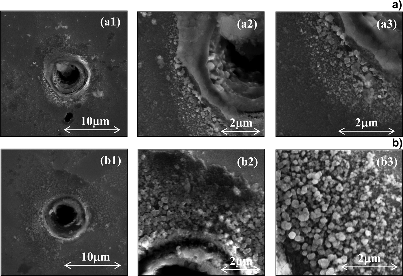
The results of the SEM analyses (Fig. 2) of the sample surface, after exposure times of 30 s and 5 min, are indicated intensive ablation of the thin film and silicone substrate from the surface of irradiated WTi/Si system. Deep craters, elevated rims and crystalline structures, inside and outside of the craters (Fig. 2) can be seen. The rims consist of compact smooth structures whereas the peripheries were composed of micro/nano-crystallites. Diameter of the nano-particles/crystallites located in the vicinity of the crater was about 200 nm and their size decreased with the distance from the rim (Fig. 2a3 and 2b3). Elevated exposure time resulted in expanding area that is covered by nano-particles. Mechanisms of crystallites formation by short and ultra-short laser ablation can be attributed to processes: direct molecule/cluster ejection after ultra-short laser pulse-material interaction, evaporation and/or collision-affected condensation in the plasma (Itina et al., Reference Itina, Gourit, Zhigilei, Noel, Hermann and Sentis2007). The elemental compositional analysis was performed by the EDX. Typical result of this analysis was presented in the Figure 3. For the case of 2 min exposure of WTi/Si surface, two spectra were recorded. Spectrum 1 corresponds to the periphery of the crater, while Spectrum 2 corresponds to its rim. Spectrum 1 has initial composition components of WTi/Si system and a peak of silicone (Fig. 3). Ration of tungsten and titanium corresponds to unmodified area and oxygen as surface contamination can also be seen. The main elements in the crater rim (Spectrum 2) were silicone and oxygen, while tungsten and titanium were not registered. Oxygen content at the rim of the crater was higher and the average enhancement comparing to the outer crater region was about 10%. This result suggests that oxygen from ambient air, during laser irradiation, made oxides with elements from the target.
Fig. 2. The effect of 20 nJ, 160 fs laser pulse on WTi/Si system. Exposure times were (a1-a3) 30 s, and (b1-b3) 5 min (LRF, 75 MHz; SEM analysis).
Fig. 3. EDX analysis: Spectrum 1 and Spectrum 2 are taken from the marked areas, after 2 min exposure time (LRF, 75 MHz; Pulse energy, 20 nJ).
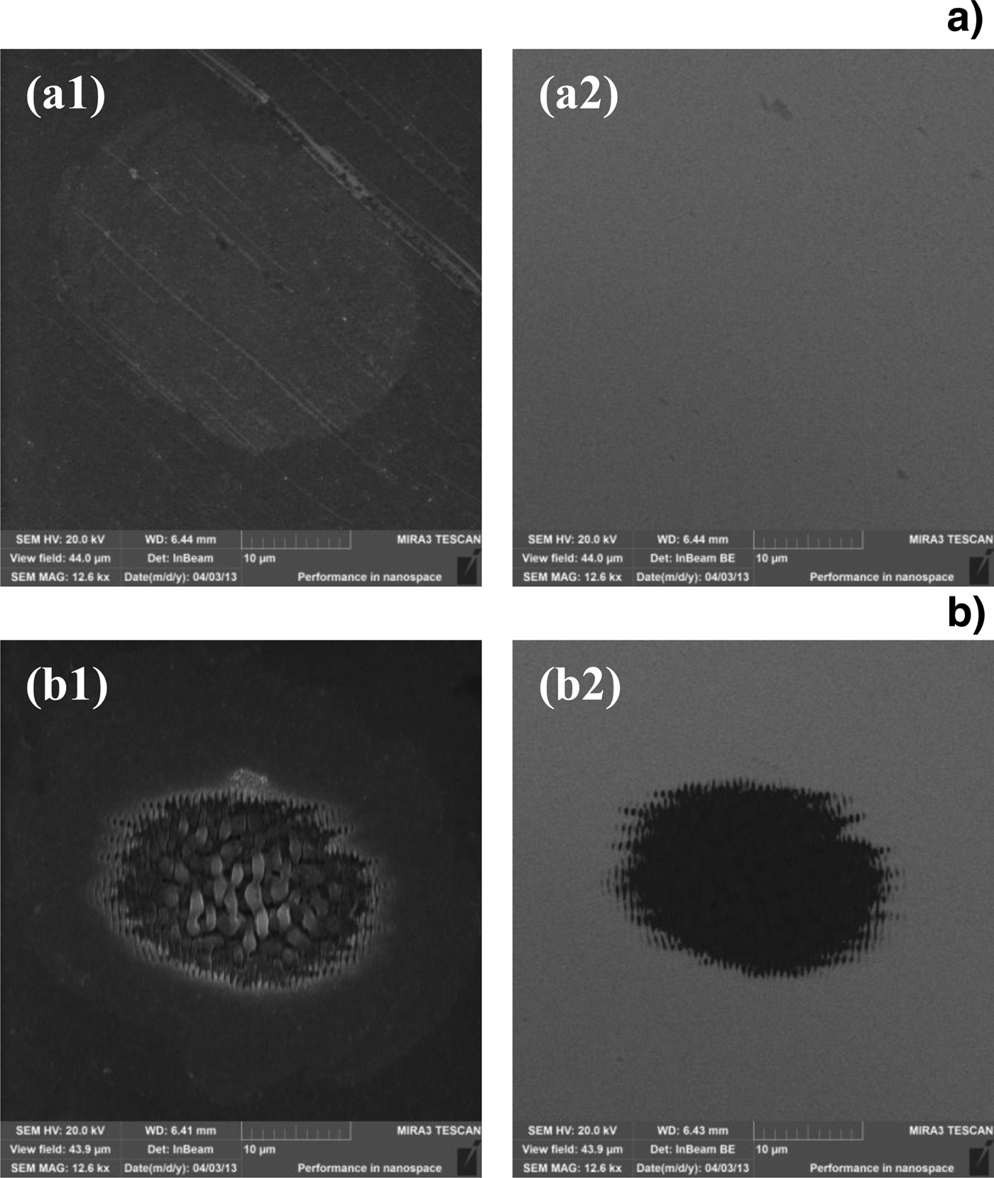
Profilometry was used in an attempt to specify deepness and geometry of the ablated areas after exposure of the surface to the high LRF radiation. This analysis was only qualitative and revealed that craters were deep with elevated rims noticeably above non-irradiated WTi/Si system surface. With the stylus profilometer the full depth of ablated areas was not achieved since depth exceeded the width of created craters (Fig. 4).
Fig. 4. Stylus profilometry of WTi/Si system after 5 min exposure time with high LRF pulses.
Femtosecond Pulse Irradiation of WTi/Si System at Low LRF
In this experiment, irradiation of the sample by the low LRF laser was done with higher pulse energies than in case of the high LRF system. Surface modification of WTi/Si target was achieved with much shorter exposure time. Accordingly, the surface modifications of the WTi/Si system were examined after 1000 laser pulses with the pulse energies ranging from 0.8 to 7.0 µJ were delivered to the same place.
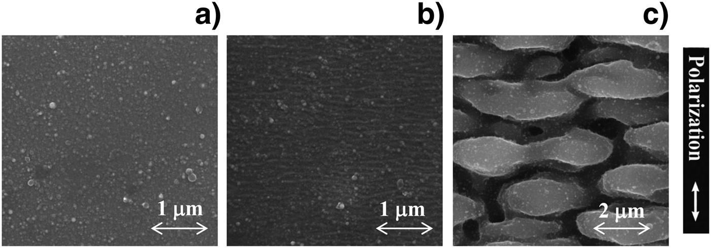
Effects of 1000 pulses at low LRF on the sample surface were recorded with two different SEM detectors (secondary electron-SE or back scattering electron-BS) (Figs. 5–7). SEM images (both SE and BS), after 1000 pulses with energy less than 2.0 µJ, did not show any surface modification. For pulse energy higher than that, surface of WTi/Si system was modified. It is shown that in the case of 2.8 µJ pulse energy, only slight morphological changes in form of LIPSSs (or ripples) were registered, without compositional changes on the WTi surface (Figs. 5.a1 and 5.a2). On the contrary, the 5 µJ pulses caused clear morphological changes with ablation of the thin WTi film from the Si substrate. Also, at the spot periphery micro-scale LIPSSs with the period close to the laser radiation can be seen (Figs. 5.b1 and 5.b2). After irradiations with higher than 2.8 µJ pulse energy, ablation with bump arrays were registered at centers of all spots. To sum up, depending on the pulse energy, SEM analysis indicates the formation of different morphological features: (1) shadow like region without thin film ablation, (2) ablated regions, (3) LIPSS, and, (4) separated bump arrays (BA) (Fig. 5 and Fig. 6).
Fig. 5. Effects of 40 fs laser pulses on the WTi/Si system. FE micrographs after 1000 pulses of low LRF radiation. Pulse energies are 2.8 µJ (a1, a2) and 5.0 µJ, (b1, b2). SE images are a1 and b1; a2 and b2 are BS images of the same area.
Fig. 6. FE-SEM micrographs of (a) as deposited WTi thin film and at centres of laser spots (Figs. 5 a1 and b1) after 1000 low LRF pulses with energy (b) 2.8 µJ and (c) 5.0 µJ, respectively.
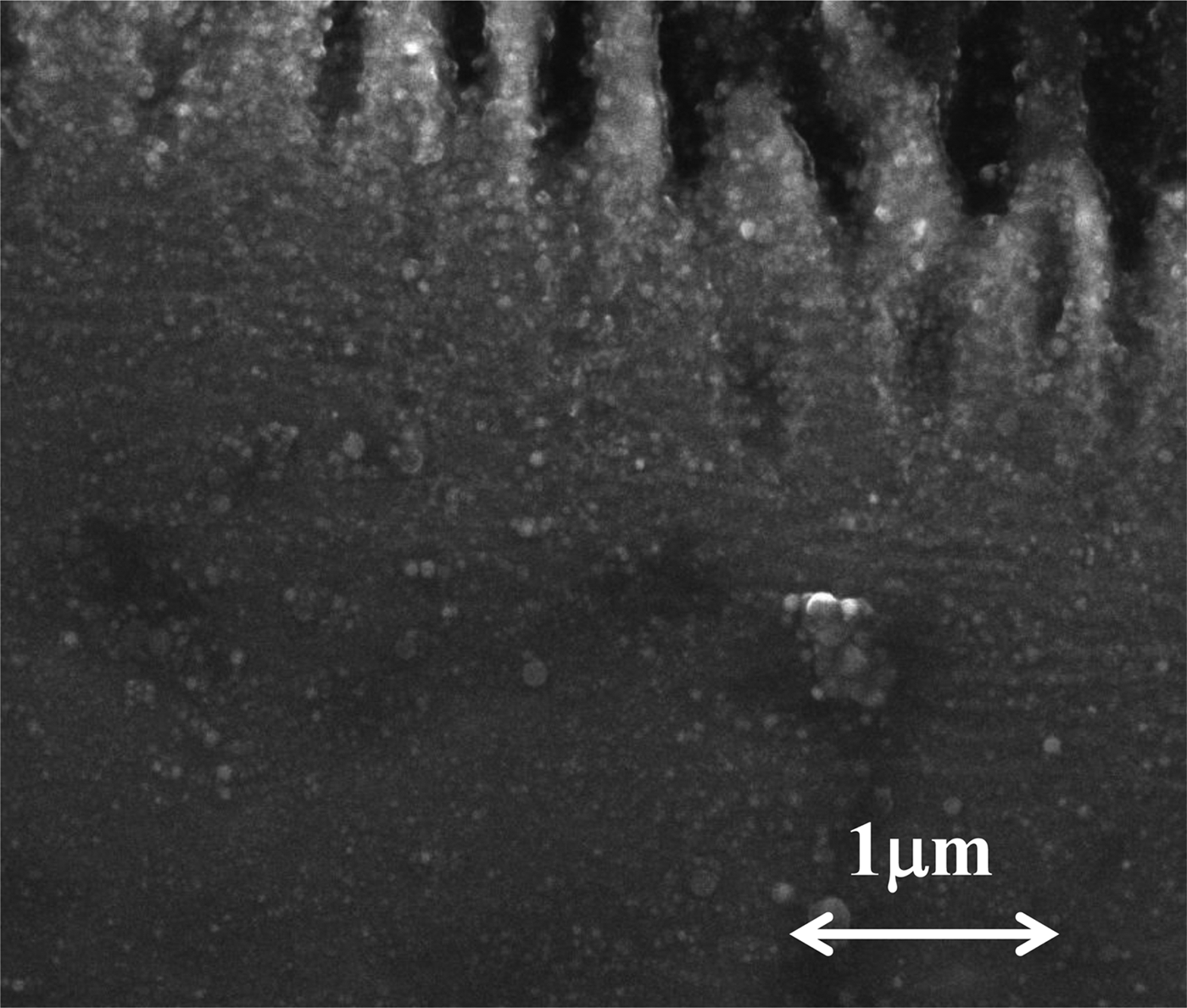
Fig. 7. FE-SEM micrographs of the spot edge after 1000 low LRF pulses with pulse energy of 5.0 µJ . Nano-scale LIPSSs parallel to the laser polarization are evident in the rectangle.
After irradiation of the relatively smooth surface of WTi thin film (Fig. 6a), with 2.8 µJ pulse energy, LIPSSs appeared over the whole spot (Fig. 6b). The created nano-scaled LIPSSs were perpendicular to the laser polarization and exhibited a spatial period of 200 nm. BAs are formed in the center of ablated area, for the pulse energy of 4 µJ and higher (Fig. 5.b and Fig. 6c), and they are mainly composed of the substrate material. Orientation of BAs was the same as formed LIPSSs and their period was approximately 2 µm. Separation of individual BAs could be result of LIPSSs
The EDX analysis, conducted in addition to the morphological examination, confirmed above statements (Table 1). On the contrary to the high LRF regime of modification of WTi/Si system, at low LRF the concentration of oxygen is reduced in the irradiated areas. The EDX analysis was performed on non-irradiated area, on LIPSS covered area on the spot edge on BA area in the spot center after 1000 successive laser pulses with pulse energy of 5.0 µJ. Formation of oxides was preferred at high LRF regime due to the pronounced accumulation effect caused by the shorter time between the two successive femtosecond pulses (13 ns) comparing to low LRF regime (1 ms).
Table 1. EDX compositional analysis of WTi/Si from three positions: non-irradiated area, LIPSS covered area on the spot edge and BA in the spot centre after action of 1000 successive laser pulses with pulse energy of 5.0 µJ
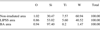
Processing option: All elements analyzed (normalized), all results in weight%.
It was reported that in case of femtosecond laser irradiation, with fluence below or close to damage threshold of investigated material, sub-wavelength periodical structures, with periods considerably smaller than laser wavelength, were observed (Her, Reference Her2010; Craford & Haugen, Reference Crawford and Haugen2007). This is confirmed in our experiment. Sub-wavelength LIPSSs, with period of about 200 nm, were created at the central area of the spot (Fig. 6.b) after 1000 successive pulses with pulse fluence of 0.39 Jcm−2 (corresponds to 2.8 µJ pulse energy). Estimated damage threshold for the WTi/Si system in the case of 1000 successive pulses was about 0.28 Jcm−2, which is close to the applied fluence.
Beside micro- and nano-scale LIPSSs oriented perpendicular to the laser polarization, we also observed nano-scale LIPSSs, with the period of about 100 nm, parallel to the laser polarization (Fig. 7). This kind of nano-scale LIPSS, registered with high magnifications during SEM analysis, appeared at the far periphery of the irradiated area. Orientation of this LIPSS may indicate that its origin is different from micro- and nano-scale LIPSSs oriented perpendicular to the laser polarization. In the literature there are suggestions what physical processes are dominant for LIPSS formation at the second and higher harmonics generation, such as field enhancement by nano-roughness, surface plasmons generation conditions, inhomogeneous deposited energy distribution, frozen capillary waves. Still, general mechanism remains an open question (Baurle, Reference Baurle2011; Her, 2011; Tsibidis et al., Reference Tsibidis, Barberoglou, Loukakos, Stratakis and Fotakis2012; Varlamova et al., Reference Varlamova, Costache, Ratzke and Reif2007; Vorobyev & Guo, Reference Vorobyev and Guo2007; Reference Vorobyev and Guo2008; Crawford & Haugen, Reference Crawford and Haugen2007; Colombier et al., Reference Colombier, Garrelie, Faure, Reynaud, Bounhalli, Audouard, Stoian and Pigeon2012; Stratakis et al., Reference Stratakis, Giorgi, Barberoglou, Dikonimos, Salernitano, Lisi and Kymakis2010; Bonse et al., Reference Bonse, Baudach, Krüger, Kautek and Lenzner2002). The reported LIPSSs with different orientation to the laser polarization, but created at once at the surface of the thin film, during the same ultra-short laser pulses radiation could be important in nano-marking/processing.
CONCLUSION
In order to investigate phenomena related to the influence of femtosecond laser pulse width and repetition frequency on the morphology of WTi/Si system we performed experiment with two laser systems, high and low LRF femtosecond laser systems. In the case of the high LRF of 75 MHz, the time between two pulses was 13 ns, while the interval for the low LRF of 1 KHz was 1 ms. As a consequence of different time interval between two successive pulses, the result was different response to the laser processing. After the high LRF irradiation for all exposure times in the experiment, the deep crater-like holes were formed with their diameters smaller than the laser beam waist. The crater rims were mainly composed of silicon and its oxide. Nanoparticles/crystalline with sizes ranging from 50 to 200 nm were generated on the spots periphery. In the low LRF regime, depending on the applied fluence, induced modifications were: (1) shadow like region without the thin film ablation, (2) ablation, (3) laser induced periodical surface structures, and (4) bump arrays. Micro- and nano-scale LIPSSs oriented perpendicular to the laser polarization as well as nano-scale LIPSSs parallel to the laser polarization were registered.
ACKNOWLEDGEMENTS
This research was supported by the Ministry of Education and Science of the Republic of Serbia, Contracts Nos. III 45016 and OI 172019. We also acknowledge the support from COST ActionMP1208.