I. INTRODUCTION
Recently, the radio frequency identification (RFID) system, operates in the ultra-high-frequency (UHF) (860–960 MHz) band to provide longer readable range and read multiple tags at speed, has gained much importance. These systems are being widely used in inventory control systems, manufacturing industries, goods flow systems, electronic toll-collection systems, etc. Generally, the RFID system uses the radio frequency (RF) signals for transferring the data to automatically identify and track tags attached to objects using a reader. Therefore, a RFID system sends a RF signal from the reader to the tag and receives a backscattered signal from the tag. In practical scenario, the RFID tags are always arbitrarily positioned and tag antennas are normally linearly polarized [Reference Nasimuddin, Chen and Qing1].
Therefore, RFID reader antennas must have circular polarized operation to ensure the reliability of UHF-RFID system. Numerous RFID antennas with circular polarization have been proposed in the literature [Reference Lu and Wang2–Reference Chen, Fu, Gong, Yan and Zhao5]. Circularly polarized (CP) radiation can be generated by exciting two orthogonal linearly polarized modes on the radiating element, with a 90° phase difference [Reference Gautam, Benjwal and Kanaujia6]. In the literature, the circular polarization in the UHF-RFID antenna was achieved by embedded asymmetric slots along the diagonal directions [Reference Nasimuddin, Chen and Qing1] and an arc-shaped strip into the square slot [Reference Lu and Wang2] of the patch antenna. In [Reference Wang, Fang, Fu and Jia3], a horizontally meandered strip and truncated corners are used to achieve circular polarization. The square patch embedded with a cross slot and an L-shaped open-end microstrip line linked to a tag-chip terminated by a shorting pin [Reference Chen, Kuo, Sim and Tsai7] and an arrowhead-shaped slot embedded in the first quadrant along the diagonal axis of a square patch [Reference Gautam, Kunwar and Kanaujia8] are also used for circular polarization. Various feeding networks can also generate circular polarization such as equal split power divider feeding [Reference Chen, Fu, Gong, Yan and Zhao5], dual offset feeding technique [Reference Chen, Sim and Kuo9], and branch line coupling along with the H-shaped slots [Reference Lai, Xie, Xie and Cen10] and the L-shaped probe-feed techniques [Reference Sim and Chi11].
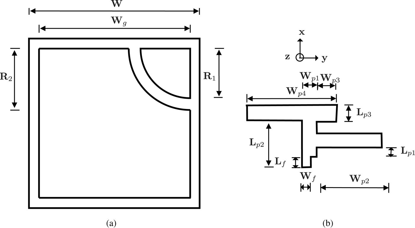
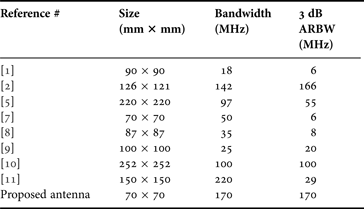
In this paper, simulation and experimental study of a CP microstrip slotted antenna has been proposed for RFID applications as shown in Fig. 1. The antenna uses a square slot antenna with a grounded arc-shaped strip to achieve the CP radiation and fed by deformed bent feeding line to obtain broad bandwidth (BW). Two near-degenerated resonant modes (TE01 and TE10 modes) with a 90° phase difference can be closely excited by the grounded arc-shaped strip on the square slot [Reference Lu and Wang2]. The recently reported antenna for RFID readers with CP operating BW at around the UHF band (902–928 MHz) are listed in Table 1. By observing these antennas, their size are greater than of the proposed one, and they have also exhibited lower impedance BW and 3 dB axial-ratio bandwidth. Notably, one antenna [Reference Sim and Chi11] offers more impedance BW as compared with the proposed antenna; however, they are achieved in the expense of smaller 3 dB axial ratio (AR) and greater size. In comparison, the proposed antenna in this investigation is simply fabricated using the low-cost FR4 substrate with a compact size with a fairly good impedance BW and axial-ratio bandwidth (ARBW). The detail of the entire design is presented in the following sections.

Fig. 1. Schematic configuration of the CP microstrip antenna for RFID applications.
Table 1. Dimensions and impedance BW and ARBW comparison of recently reported RFID antennas.

II. ANTENNA DESIGN
The proposed antenna is designed and fabricated on an epoxy FR4 substrate with a relative permittivity of ε r = 4.4 and loss tangent of 0.02. The overall dimension of the antenna is 70 × 70 × 0.8 mm3. The antenna has a simple configuration, consisting of square slot antenna with a grounded arc-shaped strip and fed by deformed bent feed-line to achieve the CP radiation. The square slot antenna with a grounded arc is etched on one side of the dielectric substrate. This insetting arc-shaped strip in the ground will disturb the surface electric field distribution on the proposed square slot antenna, a left-hand circular polarization (LHCP) performance with a wider operating BW for UHF band can be obtained. This slot antenna is evolved by cutting a square of width W g from the square of side length 70 mm. To excite two orthogonal modes with a 90° phase difference needed for CP radiation, a circular-arc strip having outer radius R 2 and inner radius R 1 is incorporated in the design. This slot antenna is fed by deformed bent feed-line formed by arranging two L p3 and one W p1 wide rectangular strips in a modified F-shaped to achieve broadband matching. To demonstrate the CP waves of the proposed antenna, the simulated surface current distributions using Ansoft “HFSS” simulator [12] at 911 MHz are plotted in Figs 2(b)–2(e), showing the direction of the distributed current at different time phases, from 0° to 135°, with an interval of 45°. The antenna is right-hand circular polarization (RHCP) when the phases are 0° and −90° for the antenna in the figure below when it radiates toward the reader, and it is LHCP when the phases are 0° and 90°. In this figure (first row), it is obvious that the current of the patch travels in the clockwise direction as increases, which results in exciting a LHCP radiation whereas the RHCP radiation can be generated by flipping the feeding structure about the y-axis (second row).

Fig. 2. Fabricated prototype of the proposed CP microstrip antenna and simulated surface current distributions at 911 MHz.
III PARAMETRIC STUDY
To understand the effects of various parameters on the proposed antenna performance, a parametric study is being employed to optimize the final design. The chosen parameters are lengths W p2 and W p4 of the deformed bent feeding line and width W g of the square slot of the antenna. The effect of the inner radius R 1 and outer radius R 2 of the arc-shaped strip on the AR is also studied.
A) Slot antenna parameters
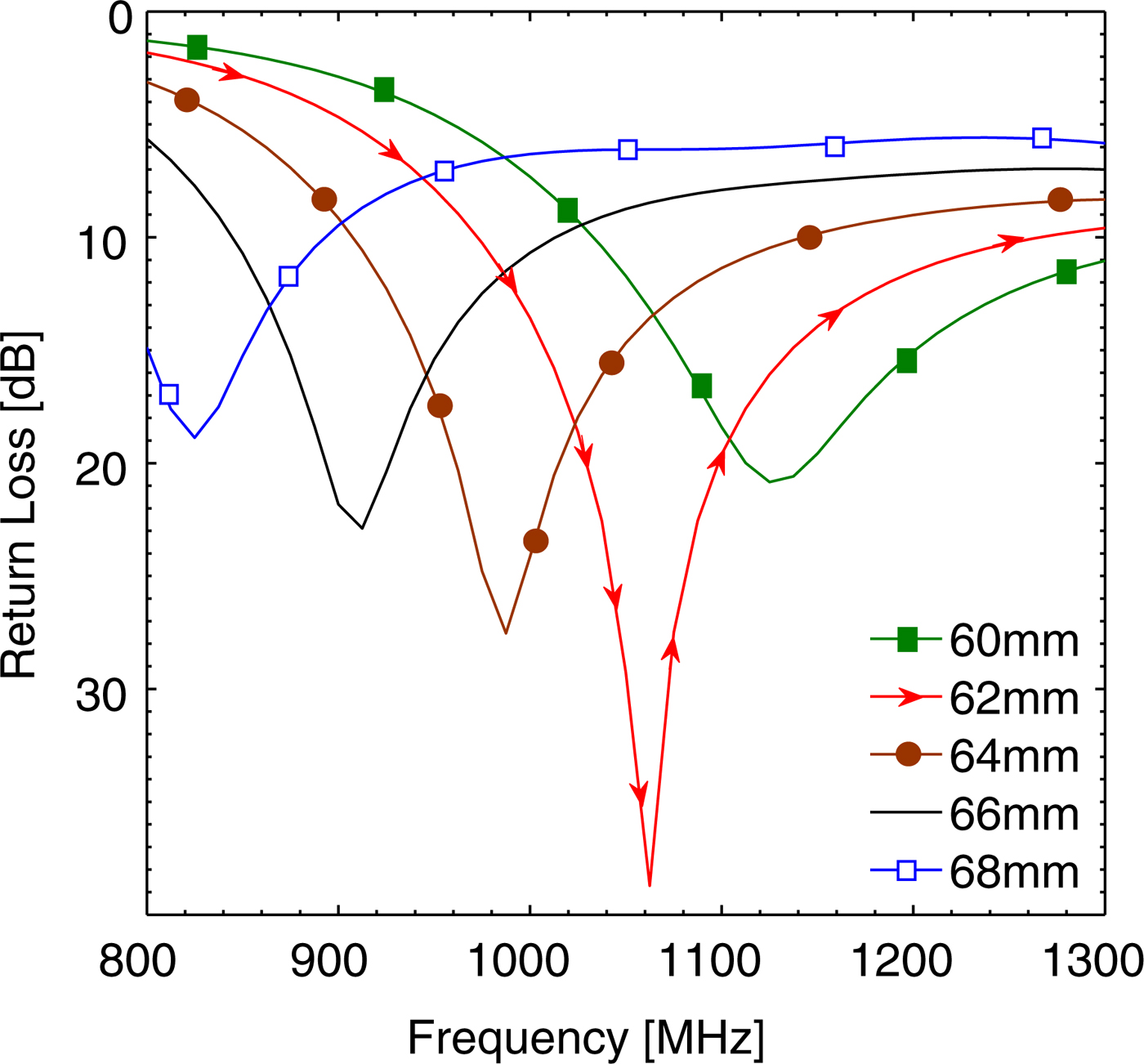
Figure 3 shows the effect of variation of the width W g of the square slot on the antenna performance. It is found that as the width W g of the slot increases, the BW remains unaltered but the resonant frequency moves toward lower side. Therefore, a width of 66 mm is taken as the optimum value for a resonance about 911 MHz.

Fig. 3. Simulated return loss against frequency for the CP microstrip antenna with various W g ; other parameters are the same as listed in Table 2. BW and ARBW = 170 MHz.
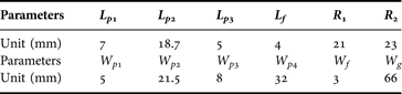
Table 2. Design parameters of the proposed CP microstrip antenna shown in Fig. 1.

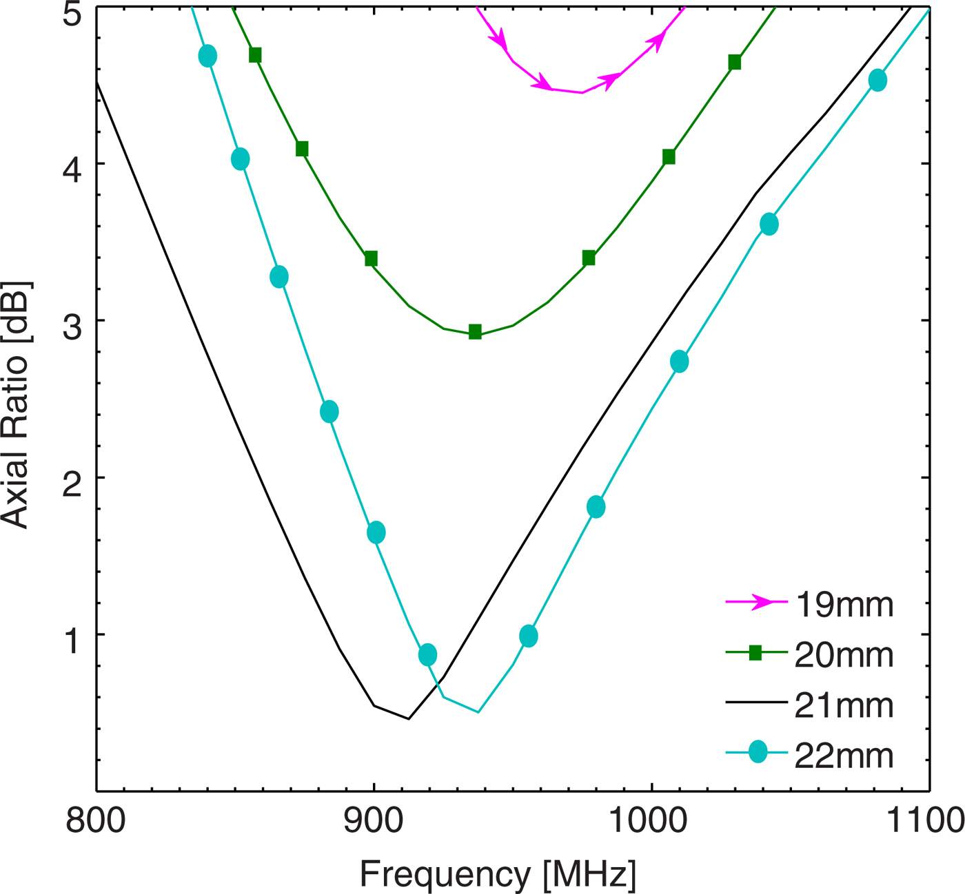
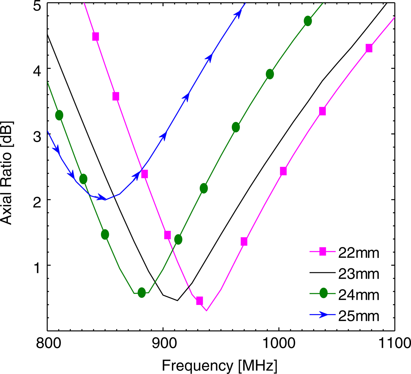
In this design, the grounded arc-shaped strip is used to generate two near-degenerated resonant modes (TE10 and TE01 modes) with 90° phase difference to form a wider CP operating BW. It can be achieved by properly adjusting the inner radius (R 1) and outer radius (R 2) of the grounded arc-shaped strip. As the arc-shaped strip generates the CP radiation, therefore, the effect of the arc-shaped strip on the AR is illustrated in Figs 4 and 5. It is observed in Fig. 4 that as the inner radius R 1 is increased from 19 to 20 mm, the quality of CP radiation starts improving with a slight shift in resonance frequency toward lower side, furthermore, the ARBW shifts toward the higher side. Thus, for a good quality of the CP radiation about 911 MHz resonance frequency, the R 1 is chosen 21 mm as the optimum. Figure 5 shows the effect of variation of outer radius R 2 from 22 to 23 mm on antenna performance. It is found that the 3 dB ARBW increases slightly with a shift in the resonance frequency toward the lower side. Furthermore, the quality of CP radiation starts decreasing. Therefore, a width of 23 mm is taken as the optimum value for a resonance about 911 MHz.

Fig. 4. Simulated AR against frequency for the CP microstrip antenna with various R 1; other parameters are the same as listed in Table 2. BW and ARBW = 170 MHz.

Fig. 5. Simulated AR against frequency for the CP microstrip antenna with various R 2; other parameters are the same as listed in Table 2. BW and ARBW = 170 MHz.
B) Feed line parameters
Figure 6 shows the effect of the width W p2 of the feed line on the return loss of the antenna. It is observed that as the length is increased from 11.5 to 31.5 mm, the operating resonant frequency shifts toward lower side with an improved impedance matching, furthermore, the impedance matching degrades. Therefore, width W p4 is chosen 25 mm as the optimum value for a resonance about 911 MHz.
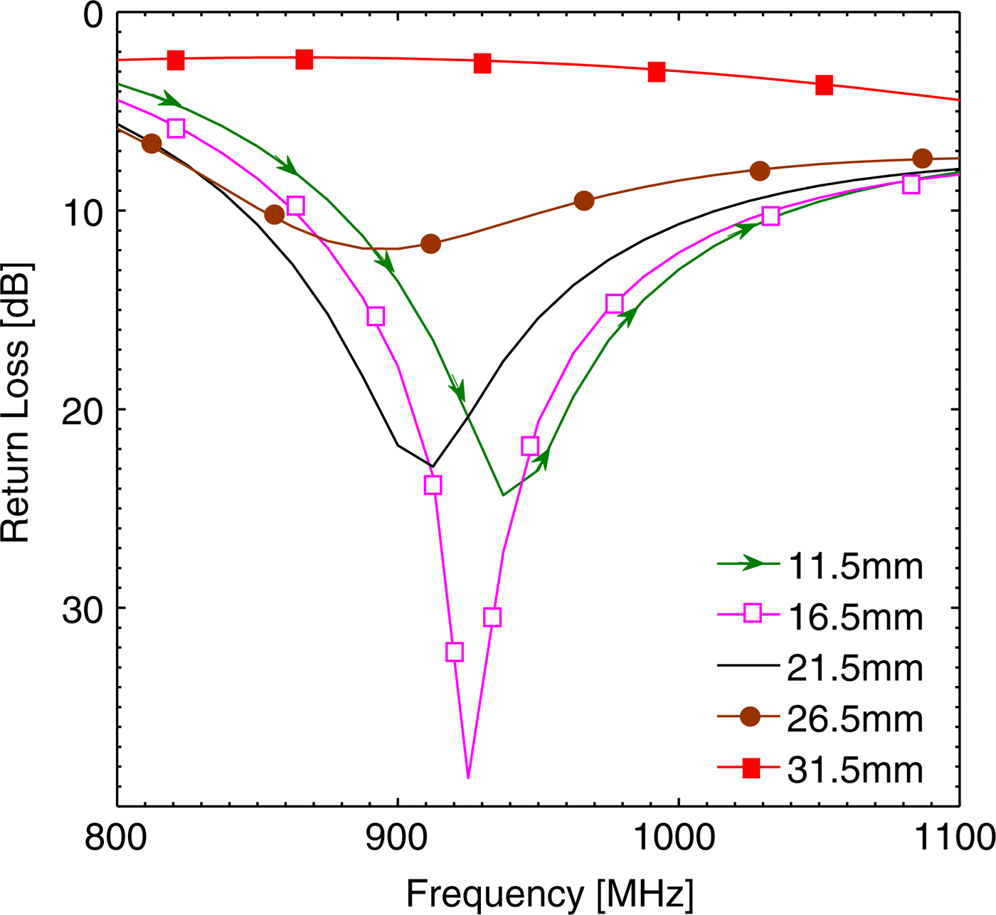
Fig. 6. Simulated return loss against frequency for the CP microstrip antenna with various W p2; other parameters are the same as listed in Table 2. BW and ARBW = 170 MHz.
The effect of the width W p4 of the feed line on the return loss is shown in Fig. 7. The simulated results show that as the length is increased from 24 to 32 mm, the operating resonant frequency shifts toward lower side with an improved impedance matching, furthermore, the impedance matching degrades. Therefore, a length of 32 mm is selected as the optimum value for a resonance about 911 MHz.
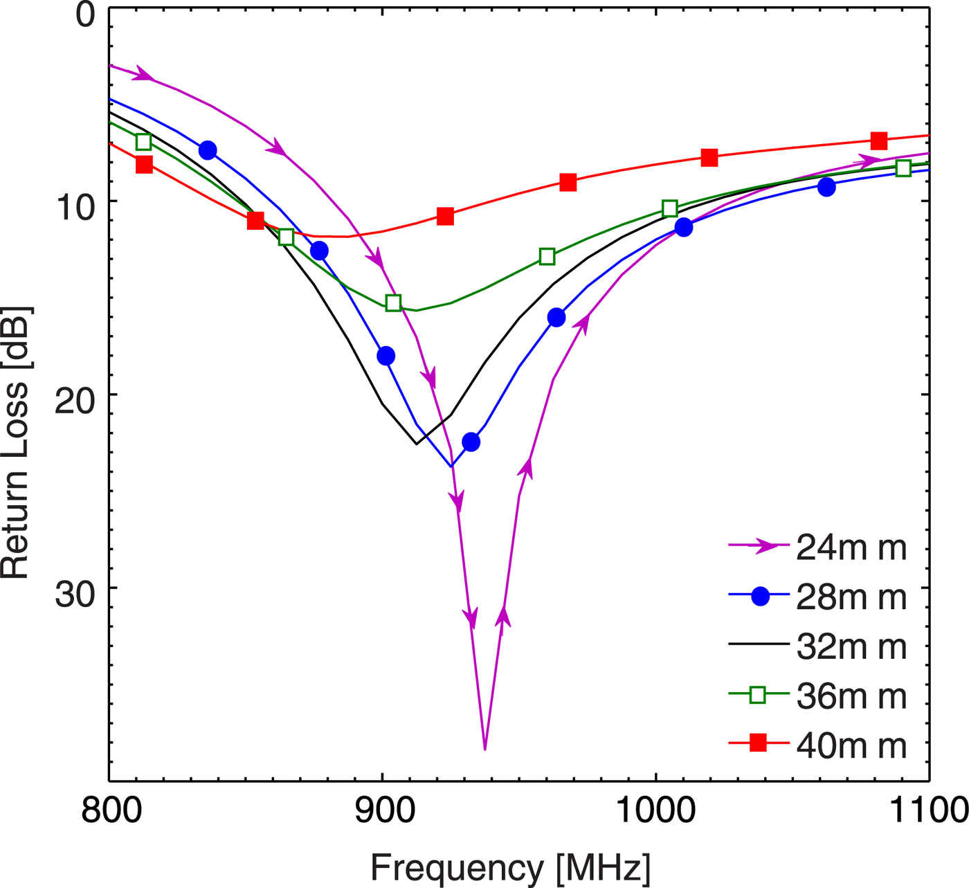
Fig. 7. Simulated return loss against frequency for the CP microstrip antenna with various W p4; other parameters are the same as listed in Table 2. BW and ARBW = 170 MHz.
IV. EXPERIMENTAL RESULTS AND DISCUSSION
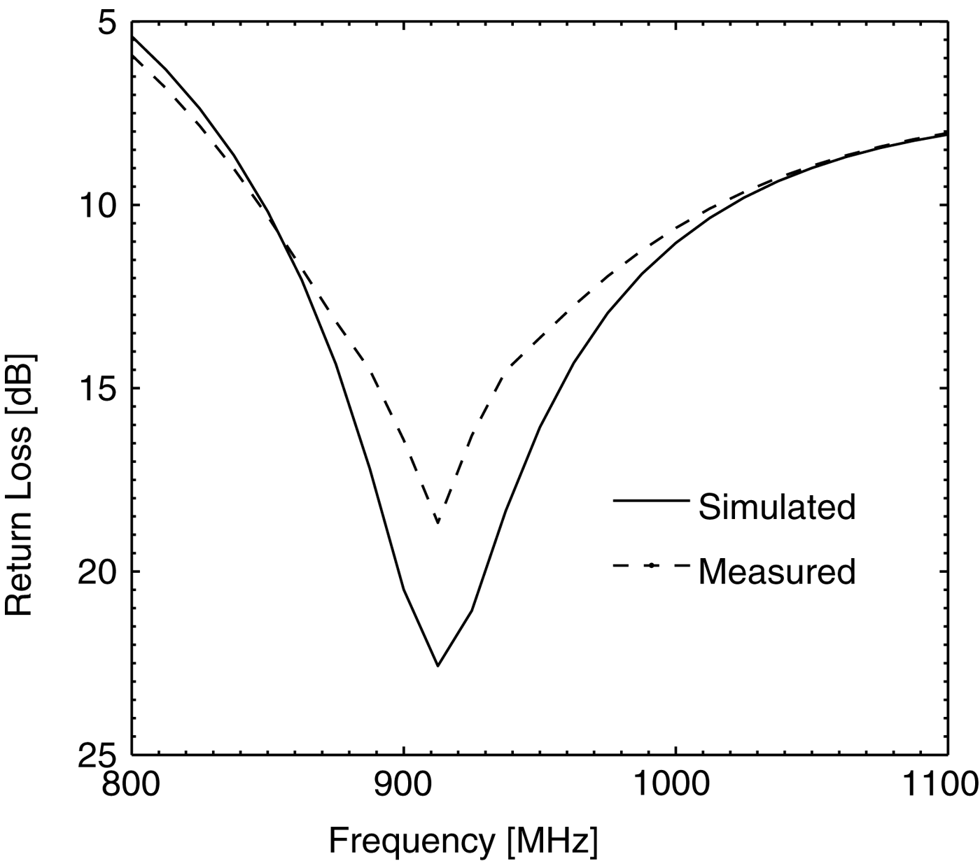
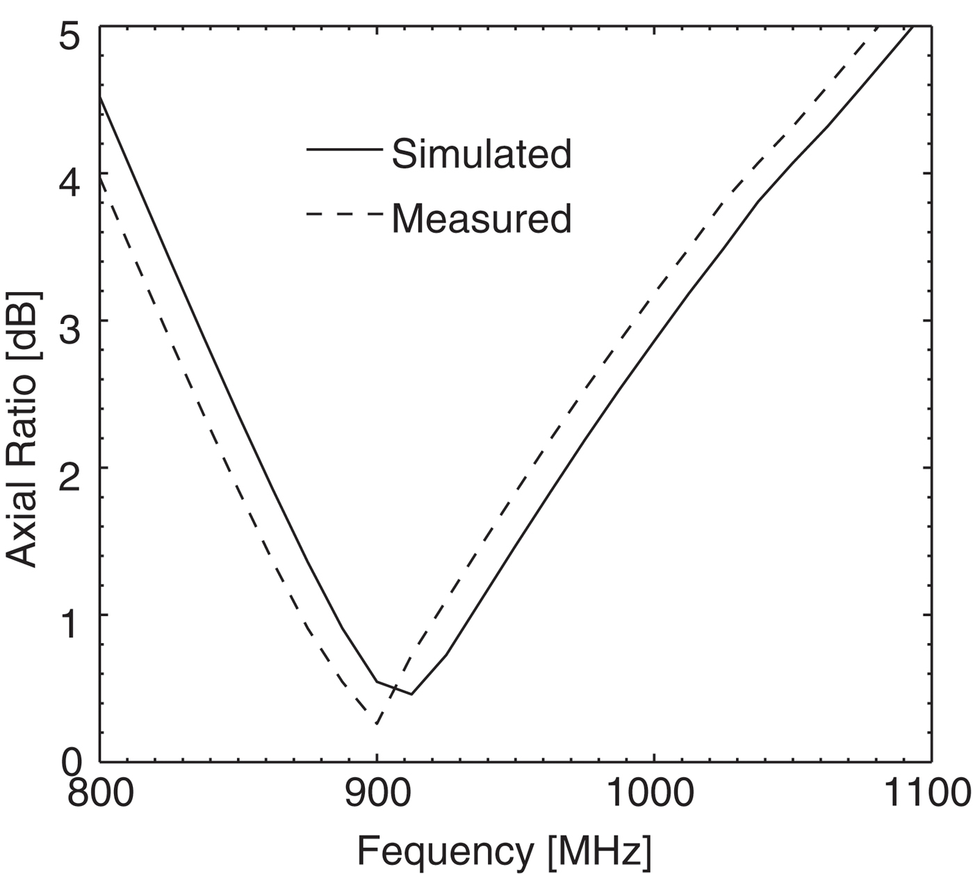
The performance of the designed antenna such as return loss, AR, and radiation patterns are measured using Agilent N5230A vector network analyzer. The measured and simulated return loss curves of the CP antenna are shown in Fig. 8. It is observed from Fig. 8 that the simulated and measured results are in good agreement. The designed antenna offers an impedance BW of 170 MHz (844–1014 MHz) which is more than earlier reported results [Reference Lu and Wang2] and evidently meets the BW requirements for the RFID systems. The measured and simulated AR at the bore-sight are compared in Fig. 9. The measured 3 dB ARBW is about 170 MHz (834–1004 MHz), and it is within the measured 10 dB return-loss BW. The simulated 3 dB AR results are in good agreement with the measured AR values.

Fig. 8. Simulated and measured return loss against frequency for the CP microstrip antenna.

Fig. 9. Measured and simulated results of the AR of the CP microstrip antenna.
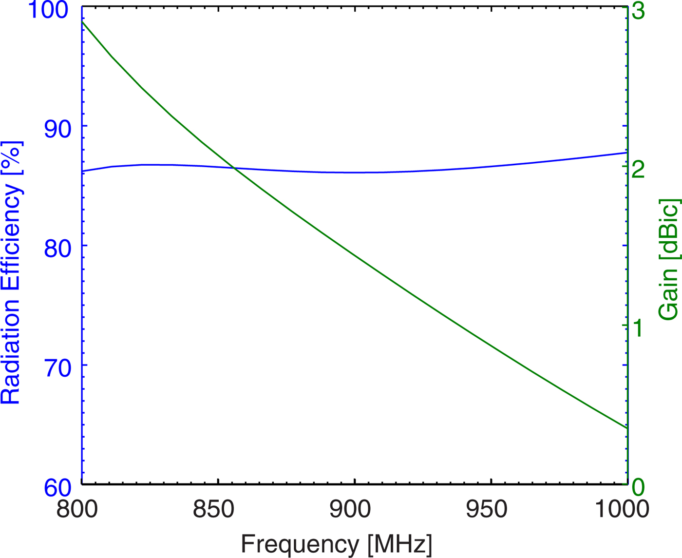
The simulated radiation efficiency and gain of the antenna are shown in Fig. 10. It is found from the figure that the antenna shows radiation efficiency of around 86% and gain varies from 2.85 to 0.45 dBic over entire operating frequency. Figures 11(a) and 11(b) show the radiation patterns of the proposed antenna. It is observed that the maximum simulated gain is 1.15 dBic at 911 MHz.

Fig. 10. Simulated radiation efficiency and gain of the CP microstrip antenna.

Fig. 11. Simulated and measured normalized: (a) Radiation patterns and (b) LHCP/RHCP radiation patterns for the CP microstrip antenna at 911 MHz.
V. CONCLUSION
A novel CP microstrip antenna for RFID applications is successfully presented and implemented. The prototype with an overall size of 70 × 70 × 0.8 mm3 achieves a 3 dB ARBW of 170.0 MHz and −10 dB impedance BW of 170.0 MHz. The proposed antenna has a smaller size and simpler design and more BW as compared with [Reference Lu and Wang2]. The proposed design is well suitable for the hand held/portable UHF-RFID reader applications.
 Neha Sharma was born in Moradabad, Uttar Pradesh, India, in 3 December 1987. She received B. Tech. degree in Electronics and Communication Engineering from IILM College of Engineering and Technology, Greater Noida (UP), India in 2011 and received his M. Tech. degree in digital signal processing from G. B. Pant Engineering College Pauri (Uttarakhand), India in 2014. His main research interests are design and optimization of circularly polarized antennas, RFID, etc.
 A K Gautam was born in NOIDA, Uttar Pradesh, India. He received the B. E. degree in Electronics & Communication Engineering from Kumaon Engineering College, Almora, India and the Ph.D. degree in Electronic Engineering from Indian Institute of Technology, Banaras Hindu University, Varanasi, India, in 1999 and 2007, respectively. He joined the Department of Electronics & Communication Engineering, G. B. Pant Engineering College, Pauri Garhwal, India, in 2000, as an Assistant Professor and he has been an Associate Professor there since 2009. Dr. Gautam is an active member of Board of study, Academic council and many other academic committees of GBPEC, Pauri. He is also member of BOS of HNB Garhwal Central University, India and Uttarakhand Technical University, Dehradun, India. He is nominated as Nodal Officer, TSP and SCSP Grants by Government of Uttarakhand and executed several projects under these grants. He has supervised 15 M. Tech. and one Ph. D. Thesis and currently supervising nine Ph.D. theses in the area of Microstrip antenna. Dr. Gautam is the author/co-author of more than 70 research papers published in the refereed international journals and conferences such as IEEE, Microwave and optical Technology Letters, Springer, etc. He is the author of the 13 books in the field of Electronics Engineering in the field of Digital Electronics, Antenna and Microwave Engineering. He is a member of IEEE (USA) and many other technical societies. He is also in reviewers panel of IEEE, Transaction on Antenna and Propagation, IEEE, Antenna and Wave Propagation Letters, IET Microwaves, Antennas & Propagation, Personal and wireless communication, Springer, International Journal of Electronics, International Journal of Microwave and Wireless Technologies, International Journal of Antenna and Propagation, etc. His main research interests are in design and Modeling of Active Microstrip Antenna, Microstrip antennas with Defected Ground Structure, Ultra wide bandwidth antennas, and reconfigurable antennas, reconfiguration antenna array, circular polarized antenna, etc.
 Binod Kumar Kanaujia currently is working as an Associate Professor in the Department of Electronics & Communication Engineering in Ambedkar Institute of Advanced Communication Technologies & Research (formerly Ambedkar Institute of Technology), Geeta Colony, Delhi. Dr. Kanaujia joined this institute as an Assistant Professor in 2008 through selection by Union Public Service Commission, New Delhi, India and served on various key portfolios, i.e. the Head of Department, In-charge Central Library, Head of Office, etc. Before joining this institute he had served in the M.J.P. Rohilkhand University, Bareilly, India as Reader in the Department of Electronics & Communication Engineering and also as Head of the Department. He has been an active member of Academic Council and Executive Council of the M.J.P. Rohilkhand University and played a vital role in academic reforms. Prior to his career in academics, Dr. Kanaujia had worked as Executive Engineer in the R&D division of M/s UPTRON India Ltd. Dr. Kanaujia had completed his B. Tech. in Electronics Engineering from KNIT Sultanpur, India in 1994. He did his M. Tech. and Ph. D. in 1998 and 2004; respectively from the Department of Electronics Engineering, Indian Institute of Technology, Banaras Hindu University, Varanasi, India. He has been awarded Junior Research Fellowship by UGC Delhi in the year 2001–2002 for his outstanding work in the electronics field. He has keen research interest in design and modeling of microstrip antenna, dielectric resonator antenna, left-handed metamaterial microstrip antenna, shorted microstrip antenna, ultra wideband antennas, reconfigurable and circular polarized antenna for wireless communication. He has been credited to publish more than 105 research papers with more than 200 citations with h-index of 10 in peer-reviewed journals and conferences. He had supervised 45 M. Tech. and three Ph. D. research scholars in the field of microwave engineering. He is a reviewer of several journals of international repute, i.e. IET Microwaves, Antennas & Propagation, IEEE Antennas and Wireless Propagation Letters, Wireless Personal Communications, Journal of Electromagnetic Wave and Application, Indian Journal of Radio and Space Physics, IETE Technical Review, International Journal of Electronics, International Journal of Engineering Science, IEEE Transactions on Antennas and Propagation, AEU-International Journal of Electronics and Communication, International Journal of Microwave and Wireless Technologies, etc. Dr. Kanaujia had successfully executed four research projects sponsored by several agencies of Government of India, i.e. DRDO, DST, AICTE, and ISRO. He is also a member of several academic and professional bodies, i.e. IEEE, Institution of Engineers (India), Indian Society for Technical Education and The Institute of Electronics and Telecommunication Engineers of India.