I. INTRODUCTION
Nowadays, cheap and reliable CMOS sub-micron processes providing devices with very high f t and f max give the opportunity to circuit designers to exploit the 9 GHz band about 60 GHz (from 57 to 66 GHz) for very high-speed wireless data communications. Because of the high absorption of the oxygen molecules around this frequency band, only short-range communications are physically feasible. A lot of research has been done and different 60 GHz receivers have been already developed using 90 nm CMOS technologies, such as OOK [Reference Kang1], sub-harmonic [Reference Kuo2], and phased array [Reference Kim3] receivers. As expected, also in this frequency band and with this technology one of the most challenging circuits is the low-noise amplifier (LNA). Beyond the requests of low-power consumption, a must for circuits thought to be used in portable devices, and wide bandwidth, essential in high-speed designs, a very low-noise figure together with very high-gain is requested to LNAs in order to improve the cleanliness of the received signal. The fulfillment of all the previous requirements can be satisfied only by a careful optimization of the transistor sizes and a precise modeling of the passive structures [Reference Hamidian, Subramanian, Shu, Malignaggi and Boeck4–Reference Hamidian, Subramanian, Shu, Malignaggi and Boeck6]. This paper presents the design of a 60 GHz four-stage fully differential LNA based on the common-source topology, using a commercial bulk 90 nm TSMC LP technology with f t and f max about 120 GHz. The amplifier has been optimized for low noise through noise matching. The rest of the paper is divided into four sections. Section II discusses the passive structures used in the design. In Section III, the design procedure is illustrated, whereas the measured results are presented and compared with the simulated values in Section IV. Section V concludes the paper with a summary and a comparison with the state of the art.
II. PASSIVE STRUCTURES
A good design of the structures used to realize on-chip inductive components is one of the keys for performing a successful mm-wave design. In this design, all the inductive elements are realized using shielded coplanar transmission lines (SCTL) [Reference Hamidian, Subramanian, Shu, Malignaggi and Boeck6]. A visual example of SCTL is given in Fig. 1.

Fig. 1. Shielded coplanar transmission line.
Such a structure has been chosen for many reasons. The grounded side walls on all the metal layers are used in order to guarantee a good electromagnetic (EM) isolation between the signal path and the other structures present on the same chip. Also, they allow satisfying, in the area close to the signal path, the technology density rules, preventing the use of metal dummy fillers that have a hardly predictable influence on the EM behavior of the circuit. Furthermore, the dense shield under the lines has been used to reduce both their losses and the influence of the low-resistive silicon substrate. The width W and the spacing S have been optimized in order to achieve high-quality factor, high inductivity and high self-resonance frequency, while the length L has been chosen in order to obtain the needed inductance value. After an optimization process, all the SCTL are designed with a width W equal to 3 µm and a spacing S of 12 µm, resulting in a characteristic impedance of 72 Ω. The design process was facilitated developing a resister-inductor-capacitor (RLC) scalable lumped model for the used structures, validated by comparison with the results of EM simulations.
III. AMPLIFIER DESIGN PROCEDURE
The common source topology is demonstrated to have better noise performance with respect to the cascode topology, especially at very high frequencies, where the mismatch between the two transistors at the middle point of a cascode amplifier is higher [Reference Malignaggi, Hamidian, Shu, Kamal and Boeck7]. Furthermore, it provides a higher output swing. Consequently, the supply voltage can be reduced to obtain lower-power consumption where a high-output power is not needed: this is the case of an LNA, which treats usually very small signals. On the other hand, a common source stage is usually not unconditionally stable.
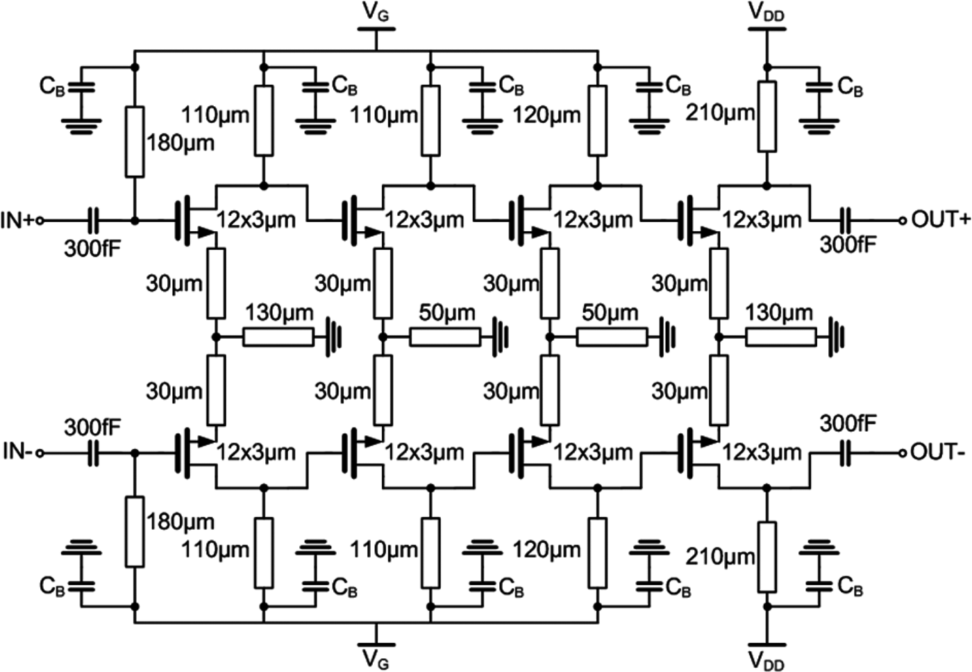
A differential structure was chosen because of all the pros given by differential circuits. A very important issue in all the high-frequency designs is the ground distribution. In fact, the ground connections between ground pads and transistors sources introduce a path that becomes very inductive at high frequencies. This problem is solved by differential configurations, where the intermediate point between the two sources of the same stage sees a virtual ground inherent in the nature of the circuit. Another noteworthy advantage of differential structures with respect to single ended ones is the common mode rejection, which gives to the differential circuits the possibility to reject a part of the common mode signal presented at their inputs. The other side of the coin is that a differential system occupies double area and consumes double power with respect to a single ended one. Taking into account all the previous considerations, a fully differential common source topology with source degeneration for better stability and source inductors for common mode rejection was chosen for the present design. The different stages have been DC-coupled, avoiding the use of DC decoupling capacitors that are the most tolerance-sensitive elements in CMOS integrated technologies. The schematic representation of the designed LNA is shown in Fig. 2.
Fig. 2. Schematic representation of the differential LNA.
The transistors and the degeneration inductors are sized in order to make possible a noise matching together with an acceptable gain, keeping at the same time the stability factor higher than the unity. Input, output, and inter-stage matching are achieved using simply a parallel SCTL, connected between the drains and the power supply. A good RF ground is obtained connecting big capacitors C B to ground after the matching inductors. Thanks to the low DC losses of the SCTL, they are used also as common-mode rejection inductances. The input and output 300 fF capacitors are used to decouple DC-wise the circuit for measurement purposes. The gate bias voltage has been chosen to guarantee the optimal noise biasing current density to all the stages, which is demonstrated to be independent on the operating frequency and the technology nodes for CMOS processes [Reference Dickson8]. The drains of the three first stages are biased together with the gates of the subsequent stages at V G = 700 mV, in order to reduce the power consumption and simplify the DC distribution, while the drain bias of the last stage are kept at 1.2 V for linearity reasons. The designed circuits are realized on chip using a 90 nm CMOS technology. Its chip micrograph is shown in Fig. 3. The chip size, pad included, is 0.38 mm2.
Fig. 3. LNA chip micrograph.
IV. MEASUREMENTS VERSUS SIMULATIONS
Large-signal, small-signal, and noise measurements have been performed on-wafer. Large-signal measurements are performed using Cascade probes with integrated balun and Rhode & Schwarz FSU67 spectrum analyzer, while small-signal measurements using GSSG Cascade probes with a differential Rhode & Schwarz ZVA67 vector network analyzer. Hot–cold noise measurements are performed utilizing the Y-factor method with a V-band calibrated Noisecom noise source and Cascade probes with integrated balun, reading the output on the Rhode & Schwarz FSU67 spectrum analyzer and following the noise figure extraction technique suggested in [Reference Abidi and LeeteCoh9]. All the measurements are carried out at the room temperature (25°C). It has to be noticed that all the results are affected by output and input pads, which have about 0.7 dB losses each [Reference Hamidian, Subramanian, Shu, Malignaggi and Boeck4]. Fig. 4 presents the comparison between simulated and measured power gain and noise figure. Owing to the good small-signal model of the transistors and to the accurate modeling of the passive components, the comparison between simulations and measurements shows a good agreement. The slight frequency shift between simulated and measured differential S21 can be mainly due to the limited accuracy of the high-frequency model of the device. The measurements show that the small-signal differential gain is almost flat in the band of interest, and achieves a peak gain of 21.3 dB at a central frequency of 57 GHz and a 3-dB bandwidth between 54.4 and 60.4 GHz. The measured differential noise figure takes values around an average value of 5.4 dB between 56 and 66 GHz. Fig. 5
Fig. 4. Small-signal power gain and noise figure: simulations versus measurements.
Fig. 5. Matching and CMRR: simulations versus measurements.
shows the matching performance, in terms of S11 and S22, and the common mode rejection ratio (CMRR) of the circuit, defined as the ratio between differential and common mode gain.
Wideband matching is achieved along with a CMRR higher than 17 dB within the 3 dB bandwidth of the amplifier. Large-signal measurements are performed to obtain the 1 dB gain compression point (P 1dB). Fig. 6 presents these measurement results at 57 GHz, performed keeping the same bias condition as the small-signal measurement. From this plot, it can be seen that the compression comes slightly earlier in measurements, due probably to some output bias issue during the measurements. The input P 1dB lays at −22 dBm input power, which means an output P 1dB of −1.7 dBm. The total power consumption is 30 mW, since 26 mA from V G = 700 mV and 10 mA from V DD = 1.2 V are drawn.
Fig. 6. P 1dB: simulations versus measurements.
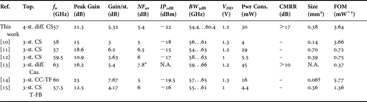
Table 1 shows the comparison between the measured performance of the presented design and the other recently published 60 GHz 90 nm CMOS LNAs ([Reference Cohen10–Reference Chang15]). It can be seen as our design is in line with the state of the art in LNA design.
Table 1. Comparison between our work and previously published 90 nm CMOS LNAs.
*Extrapolation from receiver measurements.
†Without pads.
A very well-known LNA figure of merit [Reference Song16], here reported in (1), is calculated for all the considered amplifiers and shown in Table 1. It has to be noticed that in this calculation a factor n is added for a fairer comparison, taking into account that differential topologies have double-power consumption. In fact, n is equal to 1 for single-ended circuits and to 2 for differential ones. G, F, and P DC stand for linear gain, noise factor, and power consumption, respectively.
 $$FoM = \displaystyle{G \over \lpar F - 1\rpar \lpar P_{DC} /n\rpar }$$
V. CONCLUSION
In this work, the design and the optimization of a differential four-stage 60 GHz amplifier based on a 90 nm CMOS technology is presented. For low-noise and low-power consumption, a common source topology for all the stages is chosen. The amplifier has been optimized for low-noise figure through input noise matching. In the present design, SCTL structures are used as inductive elements. Large-signal, small-signal, and noise measurements have been performed on-wafer, in order to validate the design. Thanks to the accurate modeling of all the passive and active elements, a good agreement between simulations and measurements is achieved.
ACKNOWLEDGEMENTS
The authors would like to thank GloMic GmbH for its continuous interest and support during the project. This project is financially supported by the Federal Ministry of Education and Research of Germany (BMBF) under the project frame of WiONet, Professor No. 10033322.
Andrea Malignaggi received his bachelor and master degree in Microelectronics from the University of Catania, Italy, respectively, in 2005 and 2008. After a Master of Advanced Studies in Embedded System design in ALaRI, Lugano, Switzerland, he joined the MWT group for his Ph.D. at the Berlin Institute of Technology in 2010. His main research interests are design and optimization of mm-wave LNAs and mixers in CMOS technology.
Amin Hamidian finished his studies till the bachelor degree in Electrical engineering in the University of Teheran (2006). In 2006, he joined the master program “Hardware for Wireless Communication” at the Chalmers University of Technology. He joined the MWT group in Berlin Institute of technology in 2008 for his master thesis and his Ph.D. Since 2010 he is the chip group leader in MWT Department.
Georg Boeck received the doctoral degree from Berlin Institute of Technology, Berlin, Germany, in 1984. In the same year he joined Siemens Research Labs in Munich, Germany. Since 1991, he has been the head of the Microwave Engineering Research Laboratory at Berlin Institute of Technology. He has authored or co-authored more than 230 technical papers and one book and holds several patents. He is a Fellow of the IEEE.