I. INTRODUCTION
Following the idea of Kuzmik in 2001 [Reference Kuzmik1], AlInN/GaN HEMTs for high-frequency power applications have become the new research topic in several laboratories, substituting little by little the work on AlGaN/GaN HEMTs, which are now in industrialization phase in several companies. Some publications showing very impressive power performances at microwave frequencies have been recently edited [Reference Jessen2–Reference Sarazin5], despite the fledging maturity of the processes.
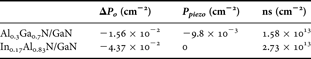
Why such interest in AlInN/GaN devices? As can be seen in Fig. 1 representing the spontaneous polarization versus the lattice constant, AlInN/GaN HEMTs have two main advantages over AlGaN/GaN HEMTs: (1) the charge induced by the spontaneous polarization is almost three times higher, allowing higher current densities. Some calculations from the equations proposed in [Reference Kuzmik6] are given in Table 1. They show that electron densities as high as 2.73 × 10¹³ can be reached in lattice matched AlInN/GaN devices. (2) As Al0.83In0.17N and GaN are lattice matched, there are no mechanical constraints in the epitaxial structures. These mechanical constraints are harmful to the reliability of the devices and are also supposed to be at the origin of trapping centers in transistors [Reference Gonschorek, Carlin, Feltin, Py and Grandjean7–Reference Neuburger9].

Fig. 1. Spontaneous polarization versus lattice constant. In AlInN/Gan devices, high spontaneous polarization is obtained without lattice mismatch between AlInN and GaN.
Table 1. Polarization and theoretical calculation of the free electron density in AlInN/GaN and AlGaN/GaN HEMTs.

In this paper we present the latest results obtained at Alcatel-Thales III–V Lab, and particularly large-signal measurement results, showing the strong potential of this new technology, and confirming the theoretical expectations [Reference Kuzmik1]. This study was done on several wafers with different processes or epitaxial growth characteristics. The impact of such differences in the processes is studied here by monitoring several electrical parameters, thanks to different characterization tools like pulsed-IV and [S]-parameters. Even if the link between physical and electrical parameters is never obvious and direct, this study gives some trends and allow us to draw some interesting conclusions, showing the advantages of this new technology as well as the points to improve.
II. EPITAXIAL GROWTH AND DEVICE PROCESSING
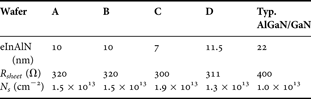
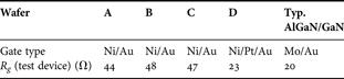
Four wafers have been characterized, named A, B, C, and D. On all these wafers, epitaxial layers were grown on SiC substrate by low pressure metal organic chemical vapour deposition (LP-MOCVD) using a 2-in. single wafer reactor. The heterostructures consist in a 1.7 µm insulating GaN buffer layer, a 1 nm thick AlN spacer layer (to enhance electron mobility [Reference Xie, Nie, Wu, Leach, Özgûr and Morkoç10]) and an undoped AlInN layer with approximately 18% of indium content (i.e. lattice matched with the GaN buffer). Different thicknesses of this layer were grown on the different wafers, as presented in Table 2. Contactless sheet resistance and sheet carrier density measurements are also reported in Table 2, for each wafer. After molybdenum-based alignment marks lift-off, ohmic contacts were formed by rapid thermal annealing of Ti/Al/Ni/Au multilayer at 900°C during 30 s under nitrogen ambient. Their average resistance was measured to be 0.15 ± 0.02 Ω mm. Argon ion implantation was used for device isolation. After electron beam lithography 250 nm Ni-based T-gates were formed by e-gun evaporation. The fourth wafer has a different gate metallization from the other ones, inducing a gate-resistance reduction by a factor 2 (cf. Table 3, the resistance values provided are measured on specific gate-metal meander line test devices). The devices were passivated with a 250 nm thick Si3N4 layer deposited by plasma enhanced chemical vapor deposition. A Ti/Pt/Au multilayer deposited by e-gun was used for interconnections. Multifinger device 3D interconnects were fabricated with plated gold bridge technology on photosensitive bisbenzocyclobutene polymer (BCB).
Table 2. Epitaxial characteristics.

Table 3. Gate metallizations and measured resistance of a gate-metal meander line test device.

The measured sheet-carrier densities n s are below theoretical expectations, presented in introduction, and do not seem correlated to the barrier-layer thicknesses on the four wafers (n s should increase with the barrier-layer thickness, as presented in [Reference Medjdoub11]). This has still not been explained, but may be due to the influence of the AlN spacer.
Despite all, it can be noted that much higher sheet-carrier densities are obtained in AlInN/GaN HEMTs than in typical AlGaN/GaN HEMTs from the laboratory, with roughly twice thinner barrier layers. Thus higher current densities are expected, as well as higher transconductance values. This last point will be discussed hereafter.
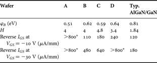
Parameters of the gate diode (i.e. the barrier height φ B, and the ideality factor η) were extracted. They are given in Table 4, as well as the reverse gate–source leakage currents at V gs = −10 and −30 V. Given the very high values of the ideality factor extracted on the AlInN/GaN HEMTs, the classical diode model is not very appropriate, and parallel resistances should be considered in order to take into account parasitic conduction modes. However, these data show the need to improve the gate processing in AlInN/GaN HEMTs.
Table 4. Gate diode parameters and current leakage.

*The measurement compliance in maximum current is reached at 800 µA/mm.
III. PULSED IV AND BREAKDOWN MEASUREMENTS
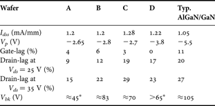
Pulsed IV and three-terminal breakdown [Reference Bahl and Del Alamo12] measurements were performed on 2 × 100 µm transistors from these four different wafers. The most important parameters extracted from these characterizations are presented in Table 5.The steady-state current I dss is expressed for V dsi = 10 V, for a quiescent bias point (V gsq = 0 V, V dsq = 0 V). V p is the pinch-off voltage of the device, measured at V ds = 5 V.
Table 5. Parameters extracted from pulsed IV measurements.

*The breakdown voltages on wafers A and D could not be well estimated due to current leakage, which alters the measurement results.
The trapping effects have also been characterized: during the pulsed measurements, the devices under test are biased at chosen quiescent points (V gsq, V dsq). As the emission of charges is very slow compared to their capture, the instantaneous current I dsi measured during pulses depends either on the quiescent voltages or on the instantaneous voltages (V gsi, V dsi). The combination of quiescent bias points used is:
(1) (V gsq = 0, V dsq = 0),
(2) (V gsq = V p, V dsq = 0),
(3) (V gsq = V p, V dsq = 25 and 35 V here).
Such IV networks measured on 4 × 75 µm transistors from wafer A are presented in Fig. 2. The gate-lag effects are quantified by comparing (1) and (2), and the drain-lag effects by comparing (2) and (3). In order to obtain a meaningful quantification of the lag effects, they are expressed in terms of potential power degradation, as detailed in [Reference Jardel13]: the achievable power is calculated, thanks to the formulation giving the theoretical output power in class A.

Fig. 2. Pulsed IV measurements of a 4 × 75 µm AlInN/GaN transistor, at different quiescent bias points: (V gsq = 0, V dsq = 0) in black, (V gsq = =Vp = −5, V dsq = 0) in dark gray, and (V gsq = −5 V, V dsq = 25 V) in light gray. Under both gate-lag- and drain-lag-related trap stress, the current keeps higher than 1 A/mm, at a knee voltage of around 5 V.
The steady-state current is higher than 1.2 A/mm in all the four wafers, whereas it is around 1 A/mm for AlGaN/GaN HEMTs processed in the laboratory. This is in accordance with the higher sheet-carrier densities in AlInN/GaN HEMTs, as presented at Table 2. The lag effects differ from wafer to wafer, but the gate-lag effects are negligible in all the wafers. The drain-lag effects induce a power dispersion estimated between 9 and 19% at V dsq = 25 V (a typical voltage for applications using 0.25 µm gate devices). The high level of current associated with the limited lag effects cause that even when the traps are stressed at such drain voltage, the current remains higher than 1 A/mm and the knee voltage as low as 5 V. Then, an estimation of the output power in class A power calculated from the theoretical formulation (P out = (1/8)I maxV max) give a result of around 6 W/mm at V ds = 25 V.
In return, the breakdown voltages are lower than in AlGaN/GaN HEMTs, for which they are around 100–110 V. This can be explained by the higher density of electrons in the channel of AlInN/GaN HEMTs, inducing higher electric field in the gate–drain area at a given bias. However, excepted for the wafer A, the measured breakdown voltages are higher than 65 V, hence allowing nominal bias voltages at 25 V or even 30 V in power applications.
IV. SMALL-SIGNAL MEASUREMENTS
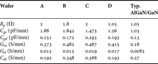
[S]-parameters have been measured at V ds = 15 V, I ds = 200 mA/mm, in order to obtain the frequency performances. They are presented in Table 6 for 8 × 75 µm devices with 0.25 µm gates. The MSG/MAG transition frequency was lower than 20 GHz on the first three wafers, preventing their use in Ku band applications. It reaches 22.5 GHz in the last one, thanks to the strong diminution of the gate resistance when a Pt diffusion barrier layer is used in the gate metallization (cf. Table 3).
Table 6. Small-signal measurements results.

Small-signal models have been extracted from these measurements in order to evaluate the correlation between the fabrication aspects and the electrical performances. Some parameters of these models are presented in Table 7. The gate resistance values extracted confirm the interest of the Ni/Pt/Au gate metallization, R g being almost divided by two in the wafer D compared to the wafers A, B, and C. This decrease of the gate resistance allows having performances comparable with classical AlGaN/GaN HEMTs processed in the lab, in terms of MSG/MAG transition frequency. In particular, the MSG/MAG transition of devices from wafer D is 7 to 4 GHz higher than the one of transistors from wafer A, B, or C. It is even 1 GHz higher than in AlGaN/GaN devices. Such improvement in the gate process is very important, allowing the use of 8 × 75 × 0.25 µm devices for power amplification at 20 GHz.
Table 7. Main equivalent small-signal model parameters.

A) Correlation between physical and electrical parameters
However, there is no clear correlation between the values of the capacitance C gs and the barrier layer thickness, which was expected to diminish with its increase. This is the case for C gd, but not in a proportional manner.
Even if the correlation between the barrier layer thickness and the intrinsic capacitances C gs and C gd remains quite unclear, there is a clear difference compared to the typical values of AlGaN/GaN HEMTs. A factor 1.45–1.8 is obtained approximately for C gs and 1.2–2.2 for C gd. The inverse phenomenon is remarkable for g m and g d, which are more or less twice lower in AlGaN/GaN HEMTs. This is totally correlated to the barrier layer thickness, which is approximately twice in AlGaN/GaN HEMTs. Calculations with first-order approximations show it very well, as detailed hereafter.
The capacitance C gs can be expressed as
where Q represents the total charge under the gate, n s the sheet carrier density, Z the total gate width, and L Geff the effective gate length.
Moreover, the drain current can be expressed as
where v sat is the saturation velocity of the electrons in the channel.
And the transconductance as
Then, it is possible, by combining equations (1)–(3), to express C gs versus the transconductance, as
Moreover,
where V p represents the pinch-off voltage, and can be expressed as:
where e AlInN represents the barrier layer thickness, and ɛ AlInN the barrier layer dielectric permittivity.
Then, (5) and (6) can be rewritten as
Equations (7) and (8) show that both g m and C gs are inversely proportional to the barrier layer thickness (the planar capacitor formulation can be recognized in equation (8)). This explains the differences of these parameters by a factor of around 2 between AlGaN/GaN HEMTs and AlInN/GaN HEMTs, the barrier layer in the latter being approximately twice thinner than in AlGaN/GaN HEMTs.
What is the impact of the g m, C gs, and C gd variations? Figure 3 shows measurements of two similar 8 × 75 × 0.25 µm transistors, one in AlInN/GaN and one in AlGaN/GaN: the marked points at 10 GHz show that the input impedances are very similar. The AlInN/GaN device shows an input reflection coefficient |Γin| = 0.81, while the value for the AlGaN/GaN device is |Γin| = 0.83. The differences in phases are due to access lines with different lengths. As a conclusion, although C gs and g m vary by a factor of 2 and ½, respectively, with respect to AlGaN/GaN HEMTs, this does not seem to have impact on the input impedance of the devices.

Fig. 3. Input impedance of two transistors with the same topology (8 × 75 × 0.25 µm), in AlInN/GaN and AlGaN/GaN. Despite the strong differences of C gs and g m, the input impedances are very similar over the (0.5–40 GHz) band. The differences in the phase were due to different access lines between the devices.
B) Frequency performances versus gate development and length
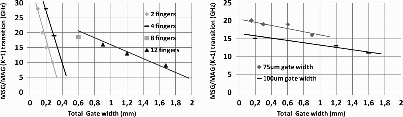
Figure 4 shows the values of the MSG/MAG transition frequency versus the total gate width of transistors from the wafer B (with Ni/Au high resistive gates) with different topologies, from 2 × 50 to 12 × 140 µm. These graphs are useful to power amplifier designers in order to help them in choosing the best topology for an application at a given frequency. It can be seen here that 8 × 75 µm devices (with a total development of 600 µm) can be used for applications at 18 GHz. The output power of such devices has to be evaluated thanks to load-pull measurements. This will be presented in a later section.

Fig. 4. MSG/MAG transition frequency of several devices with different topologies from wafer B. On the left, tendencies are traced in function of the number of gate fingers; on the right, versus the gate width. The scaling laws are well respected over a large range of gate widths.
However, these graphs also show that the transistors which would be apt for power applications at frequencies higher than 25 GHz have a relatively small total gate development (2 × 50 µm or 2 × 75 µm), hence limiting the absolute output power in amplifiers. As recapped before, the improvement of the gate resistance with Ni/Pt/Au metallizations leads to higher frequencies of operation, as approximately 5–6 GHz are gained on the MSG/MAG transition values if compared to Ni/Au gates.
Another interesting way to increase the bandwidth of these devices is to process transistors with shorter gates. Theoretically, the current gain cut-off frequency F t evolves according to an inversely proportional law with the gate length, as it can be expressed as
Figure 5 shows the evolution of F t of AlGaN/GaN and AlInN/GaN devices versus Lg−1. This graph highlights the good trend followed by F t in AlInN/GaN HEMTs, and let us suppose that reducing the gate length to 0.15 µm could lead to a further improvement of F t. Indeed, F t evolves according to the theory, i.e. the linearity between the capacitances C gs and C gd and the gate length is well respected. A theoretical line has been added in Fig. 5 that represents the values of F t calculated from the formulation of equation (9) and the values of g m, C gs, and C gd given in Table 6 for wafer D.

Fig. 5. Gain cut-off transition frequency versus the inverse of the gate length. In AlGaN/GaN devices processed in the laboratory, a saturation of f t was observed and 0.15 µm gates did not outdo 0.25 µm gates. The case of AlInN/GaN HEMTs is different, as the results fit better the theoretical law (using the formulation given at equation (9), the values of g m, C gs, and C gd of wafer D, given at Table 6, and a perfect proportionality between C gs, C gd, and the gate length).
On the contrary, AlGaN/GaN HEMTs processed in the laboratory do not show this behavior, and a saturation of F t appears when the gates are shortened below 0.25 µm, to the point that transistors with 0.15 µm gates present no advantages over those with 0.25 µm gates.
A further progress of the technology would then be to improve the frequency performances of devices will be the reduction of the gate length.
V. LOAD-PULL MEASUREMENTS
A) Cw measurements at 3.5 GHz
Measurements were performed on a 12 × 100 µm transistor from the wafer B in cw at 3.5 GHz in class A, at a quiescent drain current I ds 0 = 420 mA/mm. This wafer presents the lowest lag effects among the four wafers, and the highest breakdown voltage.
These measurements are presented in Fig. 6. A record output power of 10.8 W/mm with an associated power added efficiency (PAE) of 60% at V ds = 30 V, and a record PAE of 70% associated to an output power of 4.2 W/mm at V ds = 15 V were obtained. The linear increase of the output power versus the drain bias voltage shows the limited impact of the drain-lag on the transistors issued from this wafer. The decrease of the PAE may be explained by the fact that the output impedance set for every measurement at different drain voltages was that found for the case V ds = 15 V and was not re-tuned for other drain–source voltages.

Fig. 6. Power performances of a 12 × 100 µm transistor from the wafer B in cw, for different drain bias voltages in class A (I ds = 500 mA). The linear increase of the output power versus the drain bias voltage shows the little impact of the traps.
B) Cw measurements at 10 GHz
Load-pull measurements in cw performed on wafer A were presented in [Reference Sarazin3], and a record performance of 10.3 W/mm with 51% of PAE has been obtained at V ds = 30 V for 4 × 75 µm devices in class AB.
New measurements were carried out on 8 × 75 µm transistors from the wafer D at 10.24 GHz in cw, at I ds 0 = 300 mA/mm, and at V ds = 15, 20, 25, and 30 V (Fig. 7). For each bias voltage, the load impedance was optimized in order to maximize the output power. The maximum power obtained is 3.5 W/mm with a PAE of 51% at V ds = 15 V and 6.6 W/mm with a PAE of 39% at V ds = 30 V. The devices showed almost no ageing at V ds = 15, 20, and 25 V during the whole measurement campaign. The weak impact of the trapping effects can be attested by the limited decrease of the mean drain current in function of the input power before the gain compression, as explained in [Reference Jardel14]. Moreover, it has to be underlined that despite the fact that the technology is still under development, we noted a very high reproducibility of the measurements performed on several devices of the wafer.

Fig. 7. Power performances of an 8 × 75 µm transistor from the wafer D in cw, for different drain bias voltages (15, 20, 25, and 30 V) in class AB, (I ds = 300 mA/mm) at 10.24 GHz.
Measurements realized on wafer D has been recapitulated and plotted in Fig. 8. The results presented here are compared those of the existing bibliography published at 10 GHz, from III–V Lab and other labs since the last 4 years, to our knowledge.

Fig. 8. Inventory of published results at the frequency of 10 GHz, performances are plotted in PAE versus output power for all the labratories registered, number in brackets refers to the publication as reference.
It is interesting to notice the good results obtained, and particularly the constant increasing of performances in spite of the maturity of the technology. As for the results presented in this paper, one can notice lower performances than those published in [Reference Sarazin3]. This limitation is due to a deliberate restriction imposed on the gain compression level, in order to evaluate the devices for power amplifiers perspectives (i.e. keeping a consequent power gain at compression).
C) Cw measurements at 18 GHz
Load-pull measurements were also carried out at 18 GHz in cw on 8 × 75 µm transistors from the wafer A. Even if the max gain performances prevent the use of such devices at this frequency on this wafer, the goal was to evaluate the potentialities of the technology at high frequency. The performances obtained for the optimal load impedance for PAE are presented in Fig. 9. Indeed, it can be noted that the power gain at the maximum of PAE is equal to 6.5 dB, which needs to be improved. The reduction of the gate resistance (with new Ni/Pt/Au gate metallizations) will improve this gain, as well as the reduction of the gate length. Despite all, an output power of 34.1 dBm (2.5 W) was obtained, which corresponds to 4.2 W/mm, with a PAE of 43%. This relatively high value of PAE, as well as the negligible decrease of the mean drain current, shows indirectly the low level of drain-lag of these devices.

Fig. 9. Power performances of an 8 × 75 µm transistor from the wafer A obtained at 18 GHz in cw, V ds = 20 V, I ds = 250 mA/mm (class AB) on the optimal load impedance for PAE Z load = 12.3 + j14.1.
VI. CONCLUSION
An overview of the potentialities of the AlInN/GaN-based HEMTs processed at Alcatel-Thales III–V Lab has been presented here. Despite the fledgling maturity of the technology, the measured devices exhibit excellent power performances, even in Ku band, despite the poor gain in this case. High levels of PAE are obtained thanks to very limited trapping effects, which seem to be one of the main advantages of the AlInN/GaN compared to the AlGaN/GaN technology.
This advantage offers also the possibility to process HEMTs with higher current cut-off frequencies than AlGaN/GaN HEMTs, by developing 0.15 µm length gate devices.
Finally, AlInN/GaN HEMTs show superior performances than AlGaN/GaN HEMTs with the same technology. To be sure of their total advantage, studies on device reliability have to be conducted and degradation mechanisms to be understood. There are at the moment few data concerning these topics.
ACKNOWLEDGEMENTS
This work was supported by the EU Seventh Framework Programme FP7/2007–2011 under grant agreement no. 214610 (project MORGaN), the EU Sixth Framework Programme FP6/2002–2006 under grant agreement no. 006903 (project ULTRAGAN), and the CNES (Centre National d'Études Spatiales) under contract no. 93160.
 Olivier Jardel was born in Poitiers, France, in 1981. He received an engineering degree from Aix-Marseille I University, in 2004, and the Ph.D. degree from Limoges University in April 2008, in the common laboratory MITIC between XLIM and Alcatel-Thales III–V Lab. He is currently a research engineer at Alcatel-Thales III–V Lab, working on the development of the AlInN/GaN HEMT technology, on transistor modeling and on the design of power amplifiers.
 Guillaume Callet was born in Arles, France, in 1983. He obtained an engineering degree from ENSEA (Ecole Nationale Suprieure d'Electronique et de ses Applications) in 2008 and is currently working toward a Ph.D. degree from Limoges University, in the common laboratory between Xlim and Alcatel-Thales III–V Lab, MITIC. He works on the development of AlInN/GaN technology, particularly on the modeling of power devices.
 Jérémy Dufraisse was born in France 1985. He received the French diploma of engineer from Supelec and the master's degree in electronics from the University of Paris XI in 2009. He is currently a Ph.D. student working on developing new designs using AlGaN/GaN technology at Alcatel-Thales III–V Lab.
 Michele Piazza was born in Pordenone, Italy, in 1981. He graduated in electronic engineering at the University Of Padova (Italy) in 2008 with a thesis on reliability testing of AlGaN/GaN HEMTs grown on hybrid substrates. He is currently a research engineer at Alcatel-Thales III–V Lab and registered as Ph.D. student at X-LIM, France. He works on GaN HEMTs reliability within the Thales Microelectronics Group. His main interests are the characterization and reliability testing of Schottky diode in GaN based semiconductor devices.
 Nicolas Sarazin was born in France in 1977. He Joined the Thales Research & Technology Center in 2004 and graduated his Ph.D. degree in microwave and micro technology from the University of Lille in 2007. He is involved in AlGaN/GaN device processing and, during the last few years, has focused on AlInN based high electron mobility transistors.
 Eric Chartier received the M.Sc degree in physics from Ecole Superieure de Physique et Chimie de PARIS (ESPCI), Paris, France, in 1979. Since 1981, he has been at Thales Research and Technology Laboratory and has worked for developing transistor on amorphous then III–V semiconductors. His research interest includes microwaves measurements of transistors and MMICs.
 Mourad Oualli was born in France in 1982. He was graduated from the Ecole Polytechnique and the Ecole Supérieure d'Electricité (Supélec) in 2007. He then joined the Alcatel-Thales III–V Lab as a research engineer in the development of the AlGaN/GaN and AlInN/GaN HEMT technologies. He especially contributes to the improvement of reliability aspects by studying parasitic effects.
 Raphaël Aubry was born in France in 1973. He received the material engineering degree from ECAM Rennes in 1999, the physics master research degree from Rennes University in 2000 and Ph.D. degree from Lille University in 2004. His Ph.D. work subject was on the thermal management of the power microwave devices. He joined the THALES research center and has been working on the development of the power AlGaN/GaN HEMT technology for radar and space applications. He is currently at Alcatel-Thales III–V lab, a joint research group on III–V opto-microwave devices and power semiconductors, in charge of technology and thermal management on component based on Gallium Nitride material.
 Tibault Reveyrand was born in Paris, France. He received a Ph.D. degree from Université de Limoges, Limoges, France, in 2002. From 2002 to 2004, he was post-doctoral scientist with the Centre National d'Etudes Spatiales (CNES) (French Space Agency). In 2005, he became a contractual engineer with the Centre National de la Recherche Scientifique (CNRS), XLIM, Limoges, France. His main research interests include the characterization and modeling of RF and microwave nonlinear components.
 Jean-Claude Jacquet received the engineering degree from the Ecole Supérieure d'Optique, Orsay, France, in 1990. He subsequently joined the Central Research Laboratory of Thales, as a research staff member, where he was involved with spintronic devices. He focused his efforts on the giant magnetoresistive effect and found a new physical effect called the magnetorefractive effect. Since 1999, he has been involved with GaInP HBT and GaN HEMT microwave power devices. He is currently in charge of thermal management and of the physical modeling aspects on GaN HEMT at Alcatel-Thales III–V Lab.
 Marie-Antoinette Di-Forte Poisson obtained her Ph.D. in 1978 and joined the Central Research Laboratory of Thomson-CSF. She has been involved in the MOVPE growth, characterization and device applications of a variety of III–V compounds. Her past achievements include: the growth of high power 94 GHz InP Gunn diodes, the first realization of a linear array of a thousand pin photodiodes at 1.72 µm for the SPOT IV satellite, 980 nm high power laser diodes, GaInP/GaAs based HBT epitaxial structures for high power S band and X band amplifiers. Currently, Dr Di-Forte Poisson manages the team responsible for the “Epitaxial Growth of Wide Band-gap Materials”. She is a program committee member of the MO-VPE EUROPEAN WORSHOP and the MOVPE international conference.
 Erwan Morvan graduated in material physics and semiconductor devices at National Institute for Applied Science (INSA) in Lyon (France). He was a Ph.D. student at National Center for Microelectronics in Barcelona (CNM) from 1995 to 1999. He worked in the field of device and technology simulation. He developed an ion implantation simulator for Silicon Carbide (SiC) crystal. He obtained the Ph.D. degree in electronics from INSA Lyon in 1999. In 2000, he joined the Corporate Laboratory of Thomson CSF (LCR), now called Thales Research and Technology (TRT). He was involved in SiC MESFET design, technology, and characterization as a research engineer from 2000 to 2003. He is now involved in AlGaN/GaN and AlInN/GaN device technology research and development.
 Stéphane Piotrowicz was born in France 1971. He received a Ph.D. degree in electronics from the University of Lille in 1999. He joined the Thales Research Center and worked on the design of hybrid and MMIC power amplifiers on the InGaP/GaAs HBT technology for radar and space applications. He currently works on the development of AlGaN/GaN technology at Alcatel-Thales III–V Lab. He is in charge of hybrid and MMIC demonstrators for T/R modules as power switches, power amplifiers and low noise amplifiers.
 Sylvain Delage obtained his Ph.D. from University Paris VII in 1985 for his work carried out at CNET-Meylan on the demonstration of monolithic Si/CoSi2/Si metal base transistor grown by molecular beam epitaxy. Afterwards he was for 2 years with IBM T.J. Watson Research Center as research staff member, where he did participate to the first demonstration of Si/SiGe HBT, which later on has been developed and manufactured worldwide by major semiconductor companies.