


Introduction
With the advancement in contemporary wireless mobile communication systems, high efficiency broadband radio-frequency (RF) power amplifiers become of great importance to amplify and transmit high data-rate modulated signals efficiently. Conventional harmonically tuned power amplifiers, like class-F [Reference Hayati, Zarghami and Grebennikov1] and inverse class-F [Reference Saad, Fager, Nemati, Cao, Zirath and Anderson2], have been extensively and successfully used to realize efficient amplification techniques for narrowband signals. The narrowband nature of these power amplifiers is referred to the harmonic load resonators incorporated with the matching networks used in their construction [Reference Hayati, Zarghami and Grebennikov1]. Recently, continuous modes of operation for such types of amplifiers have been developed to achieve both broad bandwidth and efficient operation. These techniques include class-J [Reference Cripps, Tasker, Clarke, Lees and Benedikt3], continuous class-F [Reference Carrubba, Clarke, Akmal, Lees, Benedikt, Tasker and Cripps4], and continuous inverse class-F [Reference Carrubba, Clarke, Akmal, Yusoff, Lees, Benedikt, Cripps and Tasker5] power amplifiers. In the latter modes, a larger range of harmonic impedances presented to the active device is allowed, leading to wider bandwidth and more flexible design space for the circuit [Reference Chen and Peroulis6].
In the class-J power amplifier, the drain current is assumed to have a half-sinusoidal shape while the drain voltage signal is approximated by the fundamental and second harmonics with additional phase shift of π/4 between the fundamental components of the two waveforms [Reference Moon, Kim and Kim7]. This is achieved by making the fundamental harmonic impedance complex and the second harmonic impedance purely reactive at the current-generator plane of the RF power field effect transistor (FET) [Reference Wright, Lees, Benedikt, Tasker and Cripps8]. An empirical parameter is also introduced to set the drain voltage waveform in different forms with the overall efficiency kept equivalent to that of the class-B power amplifier [Reference Cripps, Tasker, Clarke, Lees and Benedikt3]. The third harmonic drain voltage component is assumed to be short-circuited by the output capacitance of the transistor, and control is restricted to the first and second harmonics. The price paid for the bandwidth improvement in the class-J power amplifier is an increase in the peak value of the RF drain voltage due to second harmonic tuning. The latter condition adds additional constraints on the power transistor's stress and breakdown voltage, requesting devices with higher drain breakdown voltages such as the GaN RF power HEMTs [Reference King and Brazil9].
Some recent studies showed that the efficiency of the class-J power amplifier is practically affected by the third harmonic impedance and can be further increased when tuning the third-harmonic component of the drain voltage in addition to the second harmonic [Reference Tuffy, Zhu and Brazil10, Reference Mimis, Morris and McGeehan11]. However, a more in-depth analysis is needed to evaluate the operation of the class-J power amplifier when contributing the third harmonic component. In this paper, a modified operation for the class-J power amplifier is described by evaluating the optimum drain voltage waveform coefficients for the first three harmonic components with both the maximally-flat and the maximum-efficiency waveforms. Based on this analysis, the equations of the desired harmonic load impedances, output RF power, and drain efficiency are formulated to show the performance improvement of the suggested mode (class-J23) over the conventional class-J power amplifier. The analysis has been verified through both ADS computer simulation and practical circuit implementation.
Theory of conventional class-J power amplifier
As stated above, the current waveform in class-J power amplifier has half-sinusoidal shape. If the power FET is assumed to be biased in a class-B mode, then the drain current is approximated by [Reference Tuffy, Guan, Zhu and Brazil12]:

where I max is the drain peak current and θ = ω 0t, with ω 0 representing the fundamental RF frequency.
The optimum theoretical drain voltage waveform with second harmonic peaking has been found to be [Reference Colantonio, Giannini, Leuzzi and Limiti13]:

where VDD is the drain bias voltage.
If a certain phase-shift angle, φ, is introduced between the drain voltage and current signals, then the above equation can be re-written as:

When φ is set to π/4 to avoid second harmonic impedance with negative real part and to make the load network realizable, the above equation can be expressed as:

By developing an empirical shaping parameter, α, the above equation can be re-written as:

The condition vD(θ) ≥ 0 is necessary to avoid driving the HEMT into the knee region which may cause severe distortion in the drain current signal. It can be shown that the peak value of the drain voltage, vD (max) = 2.9 VDD.
A simplified circuit model for the RF power HEMT with the main intrinsic and parasitic components is presented in Fig. 1, although more accurate nonlinear models are available in the literature [Reference King and Brazil9]. In this diagram, the drain impedance at three plane levels are indicated which are the drain impedance at the current generator plane Zd (Plane A), the load impedance at the intrinsic plane of the bare chip model Z′L (Plane B), and the actual load impedance at the extrinsic package plane ZL (Plane C). The nonlinear intrinsic drain to gate feedback capacitance Cgd is embedded with Cds using the well-known Miller effect. On the other hand, Cpd is the drain package capacitance and the parasitic inductance Ld stands for the drain pad and bond wires. The drain-to-source resistance Rds is relatively high and can be ignored in the analysis.

Fig. 1. Simplified circuit model for the GaN HEMT.
The first, second, and third harmonic impedances at the current generator plane are given by [Reference Wright, Lees, Benedikt, Tasker and Cripps8]:


where R opt is the optimum intrinsic load-line resistance for the traditional class-B operation and is given by [Reference Tuffy, Guan, Zhu and Brazil12]:

with Vk representing the knee voltage of the HEMT device.
Drain voltage with second and third harmonic tuning
As presented in the design theory of the class-J power amplifier, only the fundamental and second harmonic components of the drain voltage waveform are tuned, while the third harmonic component is assumed to be zero. In the following section, the optimum drain voltage waveform is evaluated when both the second and third harmonic components are taken into account.
The drain voltage waveform that is composed of the first three harmonic components can be written as:

where VDD is the drain DC bias voltage, Vd 1 is the amplitude of the fundamental drain voltage component, Vd 2 is the amplitude of the second harmonic drain voltage component, Vd 3 is the amplitude of the third harmonic drain voltage component, and θ = ω 0t.
Equation (10) can be re-written in the form:

where γV 1 = Vd 1/VDD, γV 2 = Vd 2/VDD, and γV 3 = Vd 3/VDD are known as the voltage waveform factors.
The waveform factors are to be evaluated in order to produce a drain voltage signal with maximally flat bottom [Reference Raab14] or with maximum fundamental component [Reference Raab15], where the waveform in this case contains both odd and even harmonic components. In both shapes, the drain voltage waveform should satisfy the constraint vD(θ) ≥ 0 so that severe distortion is avoided in the I–V knee region of the FET output characteristics.
The waveform factors in (11) for the maximally-flat signal can be found by successive differentiation of the drain voltage vD with respect to θ at the critical points and equating the result to zero [Reference Kazimierczuk16]. On the other hand, in order to obtain maximum drain efficiency, the drain voltage fundamental component has to be maximized. The waveform factors in this case are not easy to be determined analytically as those of the maximally flat waveform. A technique based on Fejer-Riesz's theorem of non-negative trigonometric polynomials together with the method of Lagrange multipliers can be employed to evaluate the waveform factors after converting the problem into an optimization one for maximizing γV 1 [Reference Juhas and Novak17,Reference Juhas and Novak18]. The evaluated factors for the two cases are summarized in Table 1.
Table 1. Evaluated drain voltage waveform factors

The normalized drain voltage waveforms for the two cases are sketched in Fig. 2. It can be shown that vD (max) = 3.2VDD for the maximally flat waveform and vD (max) = 3.7384 VDD for the maximum efficiency case by substituting for θ = 0 in (11) with the corresponding values of the waveform factors, revealing an increase in the peak drain voltage in the latter case due to maximization of the fundamental harmonic component.

Fig. 2. Drain voltage waveform for the modified class-J mode.
Modified operation of the class-J power amplifier
In this section, the necessary relations for finding the harmonic load impedances at the current-generator plane, output power, and drain efficiency of the proposed mode of class-J power amplifier (also may be called class-J23) are formulated based on the drain voltage and current waveforms pointed to in the previous sections. The drain voltage waveform composed of the first three harmonics can be written as:

where φ is an additional phase angle between the voltage and current waveforms contributed to the conventional 180° phase shift to avoid second harmonic impedance with negative resistance.
In a similar analysis to that clarified in the class-J mode above, if φ = π/4, then (12) can be expanded to:

This equation can also be re-written in another form after developing a similar shaping parameter, α, to make the reactive parts of the harmonic components adjustable:

where −1 ≤ α ≤ 1.
The drain voltage waveform is sketched in Fig. 3 for different values of α. It can be seen that α affects both the amplitude and phase of the drain voltage signal.

Fig. 3. Drain voltage waveform patterns for the modified class-J PA with α as a parameter.
Based on the latter equation, the harmonic components of the drain RF voltage are given by:


If the effect of the knee voltage of the HEMT is considered, then VDD is replaced by (VDD − Vk) in the above three equations. The drain current signal is defined as given in (1) and therefore the drain harmonic impedances at the current generator reference plane are evaluated from dividing the harmonic drain voltage components by their equivalent harmonic current components:

So, we have:


where R opt is given by (9) and can be tolerated to adjust the peak drain current I max in real power devices as well as to maximize the output RF power.
Although the value of third harmonic impedance is theoretically infinite due to zero third harmonic drain current, but in reality it can be of some finite value when there is a third harmonic drain current component resulting from a conduction angle >180°.
The output RF power is given by:

This equation can be formulated as

The DC input power is given by the product of drain DC voltage and current components:

The drain DC to RF efficiency is therefore found through dividing (22) by (24):

The second term in (25) represents the improvement in the theoretical drain efficiency of the modified class-J mode over that of the conventional class-J PA. It can be shown that the theoretical efficiency for the case of maximally flat waveform is equal to 83.3%, and that of maximum efficiency case reaches to about 89.8% by substituting the corresponding values of γV 1 from Table 1 in (25). Both of these figures exceed the theoretical value of the conventional class-J power amplifier due to the inclusion of the third harmonic component, with a net result of raising the fundamental voltage component. This will, however, increase the peak value of the drain voltage waveform to about 3.73VDD as illustrated in the previous section.
The drain voltage waveforms presented in Fig. 3 seem, for the first glance, similar (but not identical) to the voltage patterns obtained in the continuous class-F mode power amplifier. However, the exact drain voltage signal in continuous class-F mode, when de-factorized, contains four harmonic components that have different coefficients from those obtained in (14) with amplifier's maximum theoretical efficiency of 90.7% [Reference Tuffy, Guan, Zhu and Brazil12]. The contribution of a fourth harmonic load impedance requires devices with higher gain-bandwidth product and lower output capacitances so as not to short-circuit the fourth harmonic voltage component unless approximation is carried out by neglecting this impedance. Besides, we have introduced voltage waveform factors to control the amplitude and shape of the drain voltage signal which adds additional flexibility to reduce the signal peak amplitude at the expense of some expected loss in efficiency. Additionally, for more generalized analysis with current conduction angles other than 180°, there will be a third harmonic current component and therefore the third harmonic impedances will vary considerably since the third harmonic voltage component of the modified class-J mode is entirely different from that of the continuous class-F mode and includes both real and imaginary parts as predicted in (17).
A general comparison between the conventional and modified class-J power amplifier modes is summarized in Table 2.
Table 2. Theoretical performance comparison between conventional and modified class-J modes

Evaluation of the extrinsic harmonic impedances
In this section, explicit-form relations for the required harmonic load impedances at the drain of the device package are derived in terms of the internal model and parasitic components of the HEMT as well as the shaping parameter α. These equations are useful in estimating the actual load impedances that can, otherwise, be obtained through the harmonic load-pull test or by nonlinear embedding techniques to transform the impedances from the current generator plane into the package plane [Reference Raffo, Scappaviva and Vannini19–Reference Saxena, Rawat and Roblin21]. In order to investigate the effect of the intrinsic and extrinsic elements of the power transistor on harmonic load impedances, a real power GaN HEMT device from Wolfspeed is selected. The large signal CAD models for the packaged transistor, CGH40010F, together with its bare die CGH60015D have been used to estimate the parasitic components of the transistor. A simplified packaged model for the HEMT is presented in Fig. 4.

Fig. 4. An optimized model for the CGH40010F Packaged HEMT.
At higher microwave frequencies, additional FET parasitic elements such as the source lead inductance and resistance can be inserted for more accurate analysis. On the other hand, the intrinsic output capacitance Cds, shown in Fig. 1, is estimated from a technique adopted in [Reference Ali, Al-Muifraje and Saeed22] and is equal to 1.1 pF, where it actually includes both the gate-to-drain Miller capacitance and the drain-to-source capacitance as stated previously. Although this capacitance is usually voltage dependent and is a nonlinear element, it can be assumed linear in GaN HEMT devices with satisfactory results to simplify the analysis [Reference Mimis, Morris, Bensmida and McGeehan23, Reference Wang, Yang and Liu24].
For a drain bias voltage of 28 V, knee voltage of 4 V, and drain peak current of 1.6 A, the optimum load-line resistance is estimated from (9) to be 30 Ω. However, the value of R opt can be adjusted to control drain efficiency, output RF power, and the peak value of the drain current waveform. The theoretical drain harmonic impedances at the current generator reference plane of the power HEMT are evaluated from (19)–(21), respectively.
The effect of the parasitic elements of the drain can be investigated by referring to Fig. 1. If Rds is ignored and the drain intrinsic capacitance Cds and drain package capacitance Cpd are combined together in one equivalent capacitance, C out, then C out = Cds + Cpd. Using linear embedding technique, it can be shown that the real and imaginary parts of the fundamental harmonic load impedance ZL 1 are given by:


where ${R}^{\prime}_{{\rm opt}}$ is given by:

Similarly, the second harmonic load impedance ZL 2 is given by:

The combination of the third harmonic load impedance, ZL 3, with the inductive reactance of the drain parasitic inductance, Ld, should resonate with C out at the third harmonic frequency to present an infinite impedance at the intrinsic drain of the power HEMT, and therefore:

Figure 5 shows the effect of C out and Ld in shifting the harmonic load impedances as compared with the ideal drain harmonic impedances at the current generator plane. The output capacitance is set to 1.5 pF and the drain inductance is equal to 0.55 nH as indicated in Fig. 4.

Fig. 5. Normalized harmonic load impedances at the current generator and package planes.
Investigation of the power amplifier operation
A computerized test setup has been used to study the behavior of the proposed class-J power amplifier mode for different loading conditions as depicted in Fig. 6. In this test circuit, the CGH60015D bare-chip nonlinear CAD HEMT model, embedded with the package parasitic elements, is excited by a 50 Ω signal source. This device is biased with gate-to-source voltage of −3 V, and drain-to-source voltage of 28 V through suitable RF chokes and bypass capacitors. The circuit is terminated with the harmonic load impedances formulated in (26), (27), (29), and (30) at the first three harmonic frequencies. The voltage waveform factors are taken for the maximum efficiency case, while α is varied as a parameter. This simulation setup is implemented with the aid of the ADS microwave CAD program of Keysight.
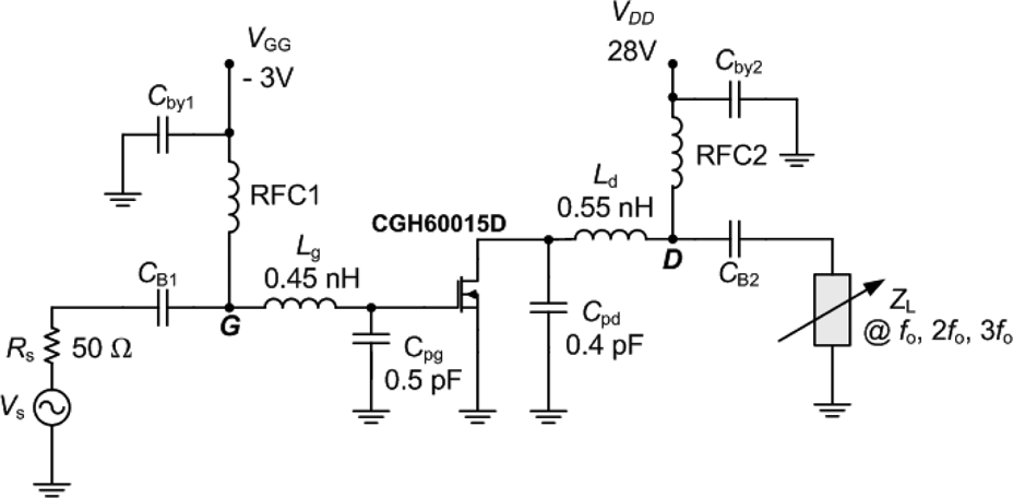
Fig. 6. Simulation setup for examining the behavior of the modified class-J PA mode.
A comparison between the drain voltage and current waveforms for the class-J and modified class-J modes is presented in Fig. 7 for a shaping parameter α = 1 and at an operating frequency of 900 MHz. In this simulation, the input driving power level is set to 29 dBm. This sketch shows clearly the increase in the peak drain voltage of the modified mode and narrower overlapping with the drain current signal. On the other hand, the drain current waveforms for both modes are close to each other, approaching to a half-sinusoidal shape. A comparison between the fundamental components of the drain voltage for the two modes of operation versus input drive power is presented in Fig. 8(a), showing a significant increase in the case of the modified mode. On the other hand, the fundamental drain current components are almost close to each other as shown in Fig. 8(b).

Fig. 7. Drain voltage and current waveforms for the class-J (a) and modified class-J (b) modes for α = 1.

Fig. 8. Fundamental drain voltage (a) and current (b) components versus input power for the class-J and modified class-J modes when α = 1.
The simulated drain efficiencies of the two modes versus drive power are sketched in Fig. 9. It is apparent that the maximum efficiency for the enhanced class-J power amplifier is more than 85% at 29 dBm input signal power, and it equals to 76% for the class-J mode at the same input power level. It is also shown from the sketch that the drain efficiency with maximally-flat voltage waveform for the modified mode lies in-between the responses of the two modes mentioned above.

Fig. 9. Simulated drain efficiency versus input power for class-J and modified class-J modes.
In Fig. 10, the simulated drain voltage and current waveforms of the modified class-J mode are sketched for α = 0 and α = −1 at 900 MHz. The shape of each drain voltage waveform in Fig. 10 resembles the corresponding theoretical pattern in Fig. 3.

Fig. 10. Drain current and voltage signals for two values of α. (a) α = 0, (b) α = −1 .
Design of a GSM power amplifier circuit
In order to confirm the proposed power amplifier mode, a typical 10 W RF power amplifier circuit has been designed based on the commercial GaN HEMT CGH40010F of Wolfspeed to operate within the GSM band from 850 to 950 MHz. Although the selected bandwidth is moderate, it is adequate to verify the theory presented thus far. The optimum load impedances at the first three harmonics are evaluated for specific frequencies in the desired band with appropriate selected values of the shaping parameter, α.
It is well known that complex impedances are only realizable when they change in clockwise direction on the Smith chart with the increase in frequency. However, for a given value of α, it can be seen from (29) that the required second harmonic load impedance is varying in anti-clockwise direction against frequency. On the other hand, the extrinsic second harmonic load impedance can be made changing in clockwise direction by decreasing α in a prescribed range as it is clear from Fig. 5. So, the range of change in the parameter α can be selected in such a way to overcome the anti-clockwise rotation of the second-harmonic load impedance with frequency [Reference Mimis, Morris, Bensmida and McGeehan23]. Based on this approach, the range for α variation has been selected from 0.8 to 0.4 with an increase in frequency from 850 to 950 MHz. Actually, the range over which α is adjusted is proportional to the operating bandwidth of the circuit, and the individual values of the shaping parameter are taken to avoid very high peak drain voltages that may drive the device near the breakdown region as predicted in (14) and Fig. 3.
For a step size in frequency of Δf, the number of evaluated frequencies in the band of interest is given from:

In this relation, f L and f H are the low and high frequency edges of the band. When f L = 850 MHz, f H = 950 MHz, and Δf = 10 MHz, then n = 10. The decrement in α for a corresponding increment in frequency is calculated from:

where α max = 0.8 and α min = 0.4.
Starting from f L = 850 MHz and α max = 0.8, and proceeding with fi +1 = fi + Δf, αi +1 = αi − Δα until f H = 950 MHz and α min = 0.4, the harmonic load impedances can be estimated from (26), (27), (29), and (30) with a load-line resistance of 30 Ω and are sketched in Fig. 11.

Fig. 11. Estimated harmonic load impedances for the frequency range 850–950 MHz.
The load network can therefore be designed to predict the harmonic load impedances presented in Fig. 11 across the desired frequency band. There are several topologies used to synthesize the output matching networks for harmonically-tuned RF power amplifiers [Reference Giannini and Scucchia25–Reference Liu, Zhang, Cheng, Li and Zhang27]. In this design, a three-section low-pass impedance matching network is synthesized analytically at the center frequency and then optimized with ADS to fit the desired impedances across the entire band. The topology of the load network is presented in Fig. 12, where the transmission line electric lengths and characteristic impedances are evaluated using a technique adopted in [Reference Ali, Al-Muifraje and Saeed22] to present ZL 1 = 23.5 + j20.25 Ω, ZL 2 = −j104.15 Ω, and ZL 3 = j30 Ω for α = 0.6 at 900 MHz.

Fig. 12. Initial design of the harmonic load network at 900 MHz.
The load network has then been optimized to predict the calculated harmonic load impedances across the entire frequency band. All the transmission lines were converted to microstrip lines based on Rogers RO4350B substrate with thickness of 1.527 mm (60 mil), dielectric constant of 3.66 and loss tangent of 0.0031 at 1 GHz. Figure 13 presents the schematic of the optimized load network while its impedance response is depicted on the Smith chart in Fig. 14. The harmonic load impedances in this sketch are almost close to the calculated values presented in Fig. 11 for the frequency band of interest. This implies that the optimized load network well fits the target theoretical harmonic load impedances.

Fig. 13. Circuit schematic of the optimized microstrip-line load network.

Fig. 14. Simulated impedances versus frequency for the optimized load network.
In order to increase the stability factor of the circuit and prevent parasitic oscillations, a stabilizing circuit consisting of a series microstrip line and a parallel RC network has been inserted at the input of the GaN HEMT. With the output matching network connected to the drain of the packaged transistor and the stabilizing circuit existing at the input port, the power amplifier circuit was simulated to evaluate the large signal input impedance across the desired frequency band at an input driving level of 29 dBm. An input matching circuit, using two-section ladder structure, was thereafter designed for conjugate matching to increase the power gain of the amplifier. The schematic of the final power amplifier circuit is shown in Fig. 15.

Fig. 15. Schematic diagram of the designed power amplifier circuit.
Circuit simulation and implementation
The power amplifier circuit has been simulated by means of the harmonic balance simulator embedded with ADS software. In Fig. 16, the drain voltage and current waveforms at the current generator reference plane of the GaN HEMT are displayed at the lower band edge, center of the band, and upper band edge, respectively. These waveforms are consistent with those presented in Fig. 3 where α is set to 0.8 at 850 MHz, 0.6 at 900 MHz, and 0.4 at 950 MHz. The drain current has an approximate half-sinusoidal shape at the three mentioned frequencies.

Fig. 16. Simulated drain voltage and current waveforms for different frequencies. (a) f=850 MHz, (b) f=900 MHz, (c) f=950 MHz.
A prototype model for the modified class-J power amplifier circuit was constructed to verify the proposed mode of operation. A printed circuit board was manufactured using Rogers RO4350B substrate with dimensions of 15 cm × 9 cm. This board was fixed tightly on a suitable aluminum heat sink using small-size screws which served also as pads between the upper and lower grounds. The RF transistor was mounted on the heat sink by means of two screws after cutting a slot on the board. The RF chocks were wounded manually using three turns of size 20 AWG wires. The RF performance of each lumped component was tested by means of the Anritsu MS4642A VNA and using suitable fixture before soldering it into the printed board. A photograph for the assembled power amplifier is depicted in Fig. 17(a). The practical test setup for measuring the performance of the power amplifier consists of a TTi TGR-1040 synthesized RF signal generator followed by a driver power amplifier module (MPA-0950 from RF Bay) to raise the signal power level at the input of the amplifier under test. A 25 W, 30 dB attenuator was connected to the output of the amplifier to attenuate the amplified RF signal before applying it to the ED PSA-3000 spectrum analyzer. The measurement setup is shown in Fig. 17(b).

Fig. 17. Photographs for the constructed power amplifier (a) and the test-setup (b).
The small signal S-parameters of the circuit are simulated and measured versus frequency in Fig. 18. It can be seen that the measured small signal gain S 21 is lower than the simulated gain by about 2.5 dB across the band of interest with an average value of 16.5 dB. Both the simulated and measured input and output return losses, S 11 and S 22, are lower than −10 dB revealing acceptable matching over the specified frequency range. The reverse gain, S 12, is shown to be better than −30 dB, thereby providing acceptable isolation between the output and input ports.

Fig. 18. Simulated and measured small signal S-parameters versus frequency.
The simulated and measured large signal performance characteristics of the power amplifier against the desired frequency range are presented in Fig. 19 for an input driving signal level of 29 dBm. No tuning process was carried out for the matching stubs to improve the practical response of the circuit. The simulated drain efficiency is changing between 82.5 and 83.5%, showing a significant improvement over the conventional class-J mode. However, the measured drain efficiency varies between 68 and 80% for different sample frequencies in the band. The mean value of the measured efficiency for the circuit is almost lower than the simulated result, but in certain frequencies it exceeds the 78.5% limit of the conventional class-J power amplifier. This sketch shows that the simulated large signal gain varies between 12 and 12.5 dB while the measured gain changes from 10.41 to 11.25 dB across the mentioned frequency range. The simulated output power is about 41 dBm at 850 MHz and drops to 40.5 dBm at 950 MHz while the measured output RF output power changes between 39.41 and 40.25 dBm. This difference between the simulated and measured response is referred to the additional parasitics and imperfections resulted from the implementation process and also to the deviation between the transistor CAD model and the actual behavior of the physical device. Additionally, there may be some reflected power from the power amplifier under test into the driver amplifier which makes the latter not working in its perfectly matched conditions.

Fig. 19. Simulated and measured performance characteristics versus frequency.
When comparing the small signal gain presented in Fig. 18 and the saturated large signal gain in Fig. 19, a considerable difference is noted because in the latter case the amplifier is heavily driven into the nonlinear region with input power of 29 dBm. This is necessary to generate the required harmonic component levels that shape the drain voltage signal properly for maximized efficiency. In Fig. 20, the simulated and measured second harmonic levels are presented against frequency. The measured response shows a second harmonic distortion lower than −30 dBc across the entire band as a result of the low pass nature of the load network.

Fig. 20. Simulated and measured second harmonic level versus frequency.
A comparison in performance parameters of the designed modified class-J power amplifier with some other recent works on the class-J continuous mode power amplifier is summarized in Table 3, revealing improved drain efficiency, η D.
Table 3. Comparison with other recent works on class-J PAs

Conclusion
A design approach to enhance the efficiency of class-J RF power amplifiers has been proposed and verified. This approach involves the incorporation of a third harmonic component to the drain voltage signal of the RF power device. The optimum theoretical drain voltage harmonic component amplitudes have been derived and the resulting relations for output RF power and maximum drain efficiency of the circuit were evaluated. Furthermore, simplified relations have been given to estimate the required harmonic load impedances at the package plane of the transistor. In order to validate the proposed mode of operation, a typical 10 W RF power amplifier circuit using a commercial GaN power HEMT has been designed, simulated, and fabricated for operation within the GSM mobile communication band from 850 to 950 MHz. The experimental results showed that drain efficiency between 68 and 80% was obtained across this band, which revealed an improved efficiency performance. Although theoretical formulas were used to expect the optimum harmonic load impedances based on a CAD device model, empirical load-pull measurement or nonlinear embedding technique can also be used to determine these impedances more accurately. Also, a more generalized analysis can be conducted when the conduction angle of the drain current signal is taken into consideration where the odd harmonics of the current waveform are no longer zero.
Acknowledgements
The authors thank Ryan Baker, of Wolfspeed, for providing them with the ADS CAD models of the GaN HEMT used in the simulation of the circuits presented in this article. They are also very indebted to the technical engineering staff at the electronic manufacturing center, industrial research and development office for fabricating the printed circuit board and assembling the prototype power amplifier model. The intensive discussions with Dr. Andrei Grebennikov of Sumitomo Electric Europe are highly appreciated by the authors.
 Firas M. Ali received the B.Sc. and M.Sc. degrees in electrical engineering from the University of Baghdad in 1994 and 1997, respectively. He worked as senior lecturer at the Polytechnic Higher Institute of Yefren, Libya from 1999 to 2011. He has been appointed as a teaching staff member at the Department of Electrical Engineering, University of Technology, Iraq since 2011. He is currently pursuing the Ph.D. degree in electronics and communication engineering at the University of Technology. His main research interest is in RF power amplifier design.
 Mahmuod H. Al-Muifraje received his B.Sc. degree in electrical engineering from the University of Technology, Iraq in 1975 and obtained the M.Sc. and Ph.D. degrees in electrical engineering from Brunel University, UK in 1979 and 1983, respectively. He worked in several Iraqi academic institutions from 1983 to 2012. In 2012, he joined the department of electrical engineering at the University of Technology as an Associate Professor. His main research interests include computer-aided design, pattern recognition, and microcomputer architecture.
 Thamir R. Saeed completed his B.Sc., M.Sc., and Ph.D. degrees in electrical engineering from the military engineering college in 1987, 1994, and 2003, respectively. He is currently a Full Professor at the Department of Electrical Engineering, University of Technology, Iraq. His research interests are digital signal processing, digital electronics and FPGA, radar signal processing, wireless sensor networks, and pattern recognition.


