I. INTRODUCTION
In recent years, the massive expansion of wireless applications and the progress of integrated radio technologies have triggered a strong interest for millimeter-wave frequencies. The large available bandwidths in these frequency bands allow the emergence of high-data rate short- and long-range wireless communications for, e.g. wireless networks, high-definition video transmission or point-to-point communications. Millimeter-wave frequencies offer also high-resolution and low-interference performance for radar and imaging applications in security, automotive, and industrial domains. The small size of millimeter-wave circuits and antennas enables a high integration density of full radio systems through cost-efficient packaging solutions. Nevertheless, large-aperture high-gain antennas are required to compensate for the high propagation losses associated to millimeter-wave frequencies and several antenna configurations can be considered to this aim [Reference Boriskin and Sauleau1]. Phased-array antennas [Reference Shin, Ku, Inac, Ou and Rebeiz2–Reference Marnat4] are a low profile and compact solution with high integration and full beamforming abilities, but they suffer from power losses in the feeding network and power consumption of active circuits (phase shifters, amplifiers); besides, they are expensive and complex to design. Waveguide-fed antennas like slotted waveguide arrays [Reference Xu, Chen and Qing5–Reference Li and Dou7] and grid arrays [Reference Zhang8–Reference Chen, Zhang, Bisognin, Titz, Ferrero and Luxey10] are low profile but suffer from frequency-dependent performances. Reflector-type antennas [Reference Hosseini, Kabiri and Flaviis11] are also a possible solution, such as reflectarrays [Reference Pozar, Targonski and Syrigos12–Reference Xia, Wu, Wang, Yu and Hong14] which are low-profile and power-efficient but have limited bandwidth and feed blockage issues.
Lenses exhibit similar radiation performances as reflectors [Reference Thornton and Huang15–Reference Al-Nuaimi, Hong and Zhang18] but do not suffer from feed blockage and allows the integration of the focal source with the RF-integrated circuits. Many lens topologies are available such as three-dimensional dielectric lenses [Reference Pasqualini and Maci19–Reference Bisognin21] which have a very high aperture efficiency and large gain bandwidth to the detriment of bulkiness, weight, and cost. Three-dimensional printing techniques offer ways to reduce cost and weight of dielectric lenses but are still limited in low-loss materials and accuracy for high millimeter-wave frequencies [Reference Yi, Qu, Ng, Chan and Bai20]. Planar lenses, such as metallic-ring Fresnel-zone plate lenses [Reference Xu, Chen and Qing22, Reference Chan, Ng and Qu23], are likewise interesting in terms of low-profile integration and cost but are characterized by a very low aperture efficiency. Other types of Fresnel lenses have interesting aperture efficiencies like the grooved Fresnel-zone lens [Reference Reid and Smith24, Reference Black and Wiltse25] or the dielectric phase-correcting Fresnel lens [Reference Hristov and Herben26, Reference Zhang27], but require complex and expensive fabrication process. Finally, discrete lenses [Reference Kaouach, Dussopt, Lantéri, Koleck and Sauleau28–Reference Dussopt30] have been proven to be attractive at millimeter-wave frequencies by demonstrating good radiation performances, large bandwidth, high aperture efficiency, beam steering capabilities and can be manufactured with low-cost processes. As all quasi-optically-fed antennas, a significant focal distance is needed to ensure optimal radiation performances, but it usually remains acceptable at millimeter-wave frequencies [Reference Kaouach, Dussopt, Lantéri, Koleck and Sauleau28].
A novel antenna architecture based on discrete-lens topology adapted for highly integrated millimeter-wave transceiver modules is presented in this paper. This work originates from our previous work where a V-band packaged transceiver with integrated focal sources was associated to a discrete lens [Reference Zevallos Luna, Dussopt and Siligaris31]. An aperture efficiency of 18% at 60 GHz and a 3 dB gain bandwidth of 12.5% (56.5–64 GHz) were obtained. However, this architecture featured an important drawback as the discrete lens and the transceiver module (with integrated focal source) came as two separate parts which needed to be mounted and aligned carefully during the system assembly.
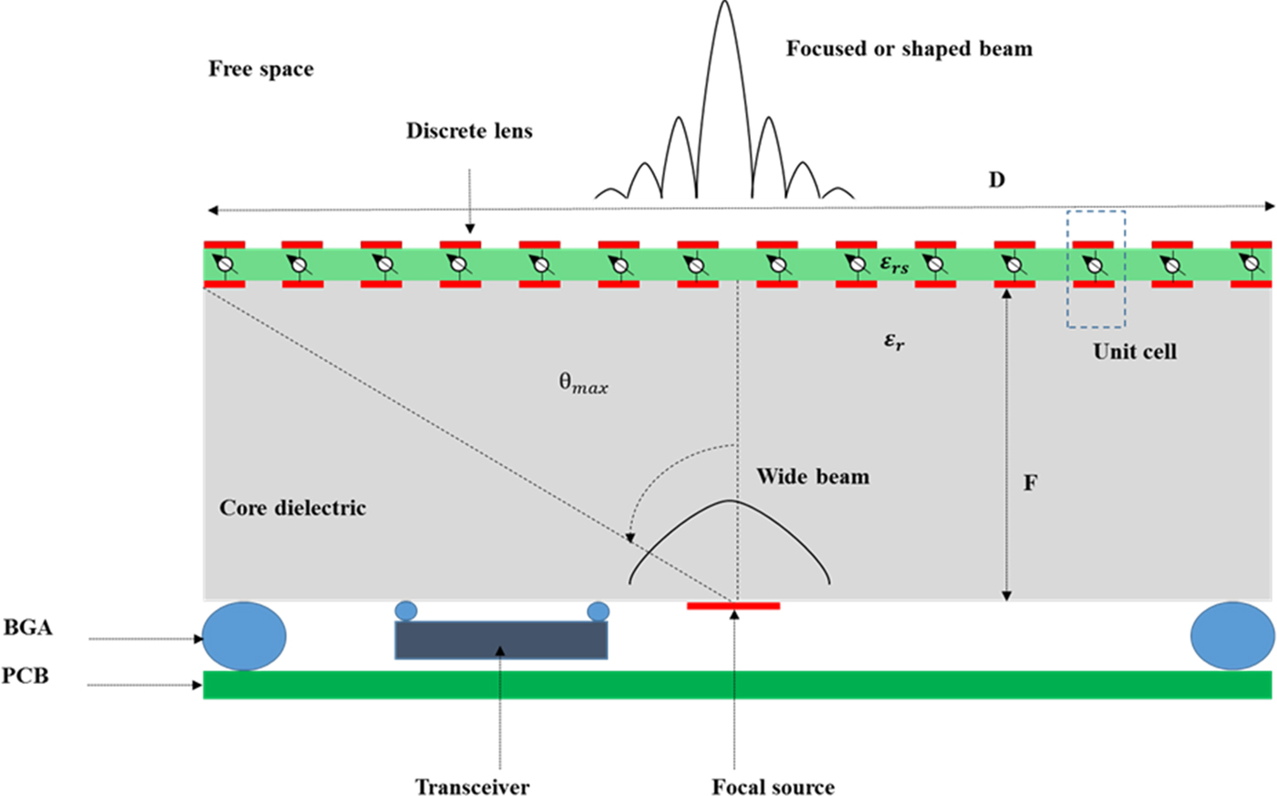
In this work, this issue is solved by mounting the discrete lens and the focal source on two opposite faces of a thick core dielectric layer, so that the transceiver module and the discrete-lens antenna can be manufactured as a single component using standard planar technologies (Fig. 1). This novel architecture exhibits a good mechanical robustness and compactness. Unlike classical architectures where they come as separate parts, the lens and the focal source can be accurately assembled at the manufacturing stage and the system assembly line is relieved from any constraint linked to the antenna. This architecture is particularly relevant at millimeter-wave frequencies beyond 60 GHz where the total thickness of the module is reduced to a few millimeters. Since the lens is now fed through a core dielectric layer, the impact on the design of the discrete lens antenna is investigated in this work. Excellent radiation performances are preserved as shown through the design of two discrete lenses based on two different unit-cell configurations, namely rotated-patch and via-less unit cells.

Fig. 1. Integration scheme of a millimeter-wave module in BGA organic technology with a transceiver integrated circuit and a substrate-integrated discrete lens antenna.
In the following, a 60 GHz waveguide-fed planar focal source radiating in the core dielectric substrate is designed in Section II. In Section III, the design of rotated-patch and via-less unit cells is presented; these unit cells enable 1-bit and 3-bit phase shift in transmission, respectively. Next, two discrete lenses are designed and optimized in Section IV-A through an in-house code and full-wave simulations; these lenses are prototyped and characterized experimentally in Section IV-B. Finally, conclusions of this work are drawn in Section V.
II. FOCAL SOURCE DESIGN
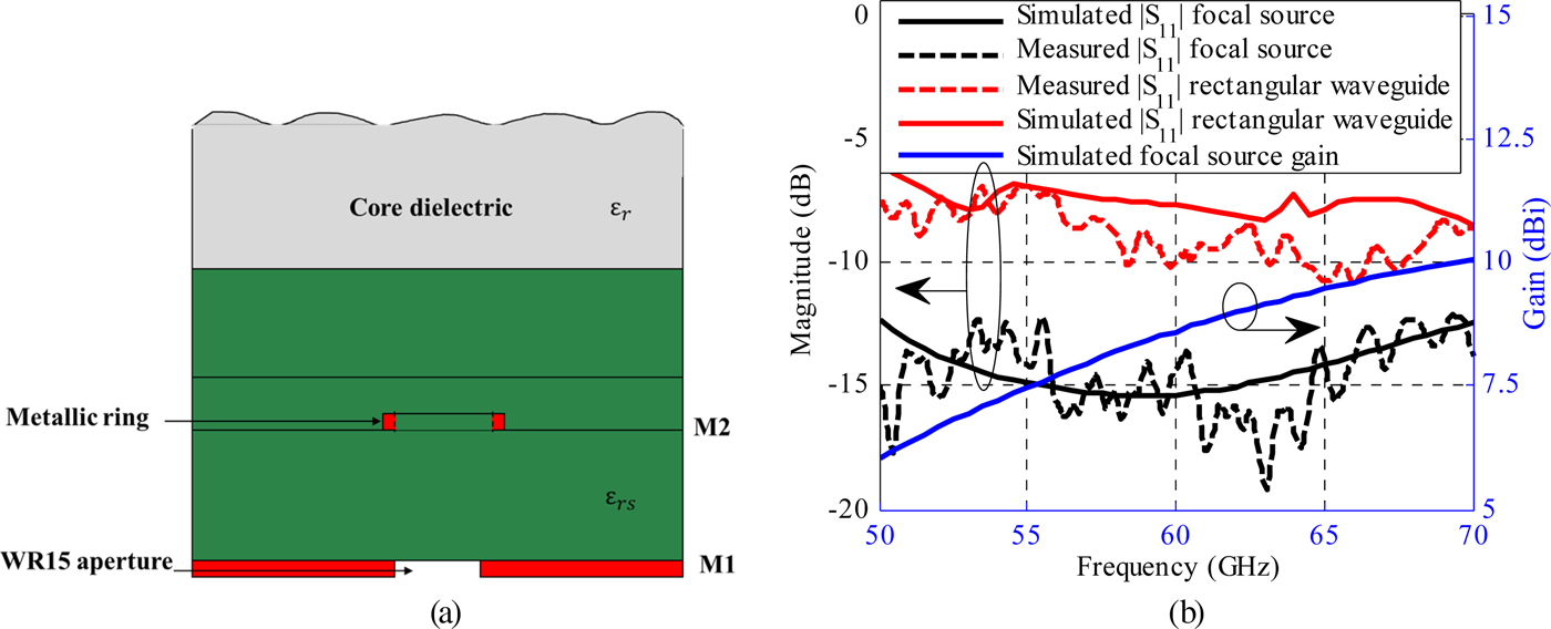
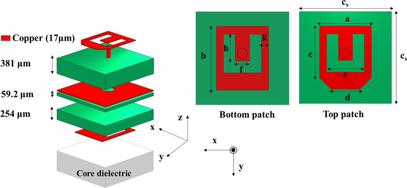
For cost-effectiveness, the same material stack is used to fabricate both the focal source and the discrete lens (Fig. 2). It is composed of three 17 µm thickness copper layers, and two Astra MT77 Isola (εrs = 3, tanδ s = 0.0017) dielectric layers of 254 and 381 µm thickness bonded by a 59.2 µm thickness prepreg layer of the same material. The dielectric constant and loss tangent of Astra MT77 are specified by the manufacturer at 10 GHz, but have shown to be quite constant up to at least 60 GHz [Reference Dussopt30]. The focal source is designed on layers M1 and M2 only (Fig. 2(a)) while the unit cells presented in the next section use the three metal layers (Fig. 2(b)).
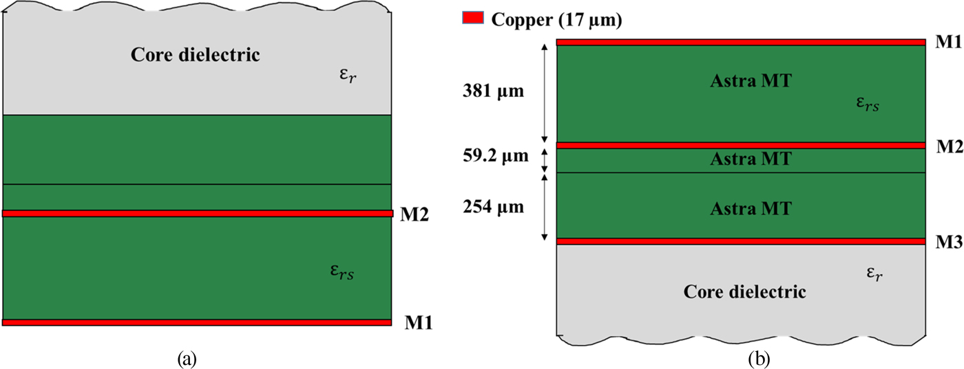
Fig. 2. Material stack, (a) focal source, (b) discrete-lens.
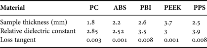
A thick plastic substrate is used between the focal source and the discrete lens as the core dielectric. Since the dielectric characteristics of most plastic materials are not available at millimeter-wave frequencies, five materials have been characterized in V-band. The characterization procedure is presented in Appendix A and the extracted properties are presented in Table 1 at 60 GHz. The PEEK material is selected for the antenna fabrication because it has low losses and its permittivity is closer to the dielectric substrate used for the unit cells (εr = 3; tanδ < 0.002).
Table 1. Plastic samples thickness and experimental extracted dielectric properties at 60 GHz.

While the final objective is to interface the focal source with a transceiver chip through a planar transmission line as represented in Fig. 1, a waveguide feed was selected here to ease the experimental tests of the discrete lens and validate the antenna concept.
As a straight transition between the WR15 waveguide and the core dielectric involves about 0.9 dB reflection losses (S 11 ~ −7.3 dB) as shown in Fig. 3(b), a planar focal source is designed for a wideband impedance matching and a wide beamwidth to illuminate the discrete lens. The radiating element is composed of two metallic layers. The bottom metallic layer (M1) is a WR15-size aperture and the top one is a half-wavelength square metallic ring on M2 coupled to the TE10 mode of the waveguide (Fig. 3(a)). The substrate thickness (381 µm) was selected for an adequate coupling to the waveguide aperture and the ring size (1.5/1.7 mm inner/outer edge length) was optimized to resonate close to 60 GHz and achieve a low reflection loss across the 50–70 GHz band. As for the unit-cells simulation, the focal source is assumed to radiate in a semi-infinite dielectric medium of relative permittivity ε r = 3 representing the core dielectric layer of the structure. The simulated and measured reflection coefficient exhibit a −10 dB impedance bandwidth larger than 50–70 GHz (Fig. 3(b)). The simulated maximum gain of the focal source is 8.6 dBi at 60 GHz; note that this gain value assumes an infinite dielectric medium and therefore cannot be measured experimentally.

Fig. 3. Cross-section of the focal source geometry (a). Simulated and measured reflection coefficient and simulated focal source gain (b).
The E and H plane radiation patterns of the focal source are presented in Figs 4(a) and 4(b) at 60 GHz, respectively. A 8.6 dBi gain and a beamwidth of 49 and 118° in H and E planes, respectively, are obtained.

Fig. 4. Simulated focal source radiation patterns at 60 GHz in (a) H plane and (b) E plane.
III. UNIT-CELL DESIGN
Discrete-lens unit cells have a typical size of 0.5–0.7 free-space wavelength in order to support only fundamental Floquet modes (these modes have no cut-off frequency) and avoid higher order modes for normal or low incidence angles [Reference Kaouach, Dussopt, Lantéri, Koleck and Sauleau28]. The lens investigated here is mounted on a thick dielectric substrate and requires to reduce the unit-cell dimensions [Reference Bhattacharyya32] according to equation (1).
 $$\displaystyle{{C_{s}} \over {\lambda _0}} \le \displaystyle{1 \over {\sqrt {\varepsilon _r} (1 + \sin (\theta _{max}))}},$$
where C s is the unit-cell size for which only fundamental Floquet modes can exist, εr is the relative dielectric constant, λ 0 the free-space wavelength, and θ max the highest incident angle impinging the unit cells (at the edge of the lens). The core dielectric substrate between the focal source and the discrete lens is a plastic-type material with a relative permittivity of 3. The nature and the dielectric characteristics of the actual material used for the antennas investigated here will be discussed in Section III. θ max is related to the diameter of the discrete lens (D) and the focal distance (F) through equation (2).
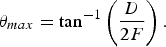 $$\theta _{max} = {\rm ta}{\rm n}^{ - 1}\left( {\displaystyle{D \over {2F}}} \right).$$
Figure 5 shows the maximum incident angle θ max and the unit-cell size C s as a function of the focal ratio F/D using (1) and (2). The focal ratio F/D is usually chosen as a trade-off between the antenna height and the optimal illumination of the lens to achieve the highest aperture efficiency. For typical focal sources like patch antennas, horns and open waveguides, the focal ratio is in the range of 0.4–0.6 [Reference Kaouach, Dussopt, Lantéri, Koleck and Sauleau28]. In the following, a focal ratio of 0.4 is selected, corresponding to a maximum incidence angle of 52° and a maximum cell size of 0.32λ 0.
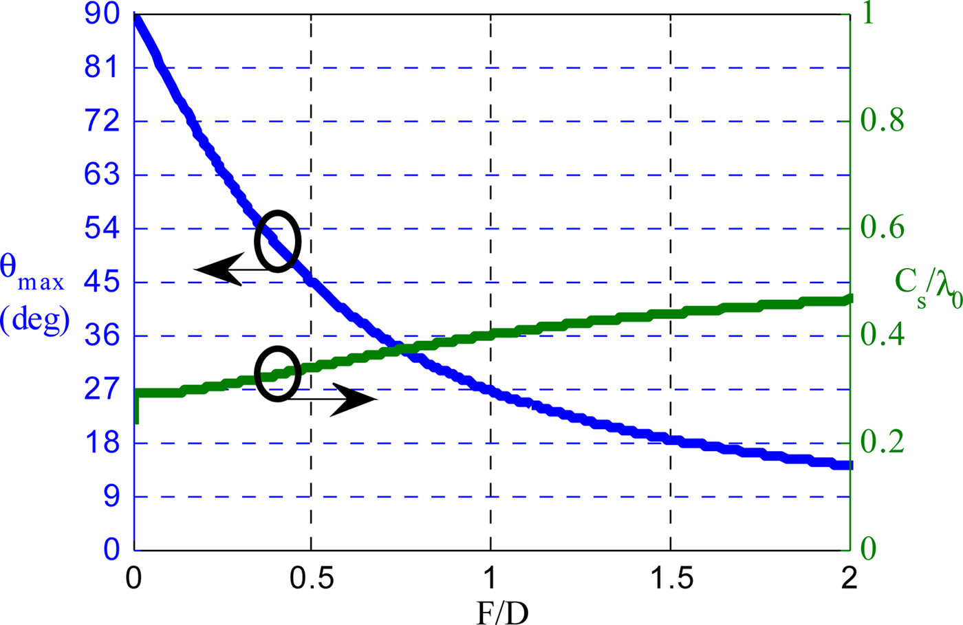
Fig. 5. Maximum incidence angle and unit-cell size as a function of focal ratio for εr = 3.
As mentioned in the introduction, two kinds of unit cells, namely rotated-patch and via-less unit cells, are investigated and presented in the following Sections III-A and III-B.
A) Rotated-patch unit cell
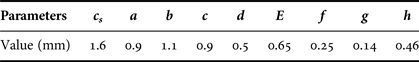
This first unit-cell geometry is presented in Fig. 6. It is made of two linearly polarized U-slot patch antennas printed on the top and bottom layers, and interconnected by a 100 µm diameter via. The intermediate metallic layer acts as a common ground plane for the two patch antennas. A 300 µm diameter aperture is etched in the ground plane around the via connection. The unit-cell geometrical dimensions have been chosen according to the manufacturing design rules and are summarized in Table 2. The cell size is smaller than a third of a wavelength with 1.6 mm × 1.6 mm (0.328λ 0 × 0.328λ 0 at 61.5 GHz). With a rotation of the upper patch around the central via by 180°, a 180° phase shift is obtained for the radiated signal. This scheme enables the design of 1-bit linearly polarized discrete lenses using 0 and 180° unit cells. Its advantages are the compactness of the unit-cell and the similar S-parameters and radiation performances of both phase states. Other patch rotation angles would allow a finer phase resolution but would lead to a circularly polarized discrete lens using the sequential-rotation principle. Such schemes have been demonstrated in previous works [Reference Kaouach, Dussopt, Lantéri, Koleck and Sauleau28, Reference Zevallos Luna, Dussopt and Siligaris31].

Fig. 6. Linearly polarized rotated-patch unit-cell geometry (dimensions given in Table 2).
Table 2. Linearly polarized rotated-patch unit-cell dimensions.

The unit-cell simulation is performed with Ansys-HFSS using periodic boundary conditions and Floquet ports. The core dielectric below the bottom patch antenna is assumed to be semi-infinite. The S-parameters of 0 and 180° unit cells under normal incidence are presented in Figs 7(a) and 7(b). A reflection coefficient lower than −10 dB is obtained over a bandwidth of 23% (54.5–68.5 GHz) and a 1 dB transmission bandwidth of 30% (51.5–70 GHz). The unit-cell insertion losses are very low with 0.26 dB at 60 GHz. Simulations under oblique incidences up to 52° showed stable responses.
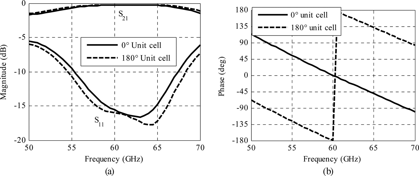
Fig. 7. Linearly polarized rotated-patch S parameters of 0 and 180° unit cell. (a) Transmission and reflection magnitude, and (b) transmission phase.
The unit-cell radiation patterns are also simulated with Ansys-HFSS by replacing the top (free space side) or the bottom (dielectric core side) Floquet port by a radiation boundary condition in order to obtain the top or bottom patches radiation patterns, respectively. The radiation patterns at 60 GHz in E and H planes of the 0° unit-cell bottom and top patch antennas are shown in Figs 8(a) and 8(b) (180° unit cell has identical radiation patterns). The radiation gain and 3 dB beamwidth of the bottom patch antenna are 5.6 dBi and 80 × 80°, respectively. In contrast, the top patch antenna radiates in air so that its electrical area is three times smaller (the relative dielectric constant of the core dielectric substrate equals to 3); accordingly, its gain is reduced to 0.9 dBi and beamwidth enlarged to 125 × 125°. The cross-polarization levels are below −45 dB over all angles in both E and H planes.
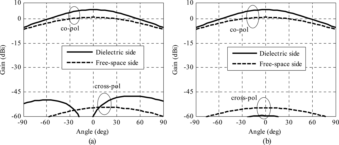
Fig. 8. Top (free-space side) and bottom (dielectric side) linearly polarized rotated-patch unit-cell simulated radiation patterns at 60 GHz. (a) H plane, and (b) E plane.
B) Via-less unit cell
In order to avoid via connections, which can be bulky at millimeter-wave frequencies, via-less unit cells have been designed on the same substrate stack presented in Fig. 2(b). In contrast to coupled-resonators designs where metal layers are separated by about quarter-wavelength distances, the thin substrates (0.12λ g) here limit the achievable transmission phase range.
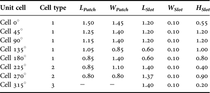
Three types of unit cells have been designed to provide eight-phase states while keeping a good transmission magnitude over the 57–66 GHz bandwidth. The design of such unit cells is more difficult than with the rotated-patch scheme since each unit cell has to be optimized individually for the specific transmission phases. The unit-cell geometries are presented in Fig. 9 and Table 3. The cell size is identical to the rotated-patch design (1.6 mm × 1.6 mm).

Fig. 9. Linearly polarized via-less 3-bit unit-cells geometry (dimensions given in Table 3).
Table 3. Via-less 3-bit unit-cells dimensions (in mm).

The type-1 unit cells provide the 0, 45, 90, 135, 180° phase states and are composed of identical top and bottom rectangular patch antennas coupled through an H coupling slot in the intermediate metallic layer (M2). Type-2 unit cells provide the 225, 270° phase shifts. For this cell type, the H coupling slot is replaced by a double slot. The 315° phase state is obtained with the type-3 unit cell only composed of an array of five slots in the middle layer (M2). The eight-phase states are obtained with the unit-cells dimensions reported in Table 3.
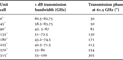
The eight unit cells defined in Table 3 are simulated using Ansys-HFSS software with periodic conditions and Floquet ports under normal incidence. Oblique incidences up to 52° were also considered and did not affect significantly the unit-cell performances. The transmission magnitude and phase are presented in Figs 10(a) and 10(b) and summarized in Table 4.
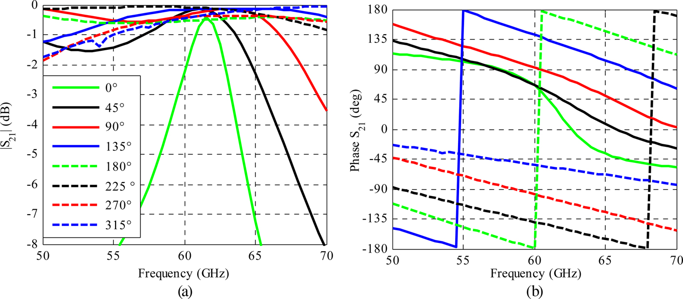
Fig. 10. Via-less 3-bit unit-cells transmission coefficient: (a) magnitude and (b) phase.
Table 4. Via-less 3-bit unit-cells transmission characteristics.

The eight unit cells demonstrate a wide (>30%) 1 dB transmission bandwidth except for the 0° (3.6%) and the 45° (12%) unit cells. This may be due to the fact that to achieve these two phase states with the type 1 unit cell, the top and bottom patches are large resulting to a resonant behavior close to the lens operating frequency. The eight unit-cells insertion losses are between 0.1 and 0.5 dB. It is also important to notice that the actual transmission phase of the unit cells is not uniformly distributed. These two issues are addressed in the lens design by selecting an optimal phase distribution maximizing the phase shift range covered by the unit cells and minimizing the number of 0 and 45° unit cells. Thanks to the careful selection, it will be demonstrated in the lens design that the phase error losses remain quite low.
IV. DISCRETE LENS DESIGN AND CHARACTERIZATION
A) Discrete lens design
Using the unit cells and the focal source presented above, the focal distance and the lens phase distribution were optimized using an in-house code. Based on our previous works [Reference Kaouach, Dussopt, Lantéri, Koleck and Sauleau28], the code was modified to take into account the dielectric substrate between the focal source and the discrete lens. This is done using a general expression of the Friis equation to calculate the transmission between the focal source and each unit cell of the lens. The wave received by the i-th cell is expressed as:
 $$a_1(i) = \sqrt {P_1} H_{fs}(\theta _i,\varphi _i)H_{Rx(i)}(\theta _i,\varphi _i)\displaystyle{{\lambda _g} \over {4\pi d(i)}}e^{ - \displaystyle{{2j\pi d(i)} \over {\lambda _0/\sqrt {\varepsilon _{r(1 - j\;{\rm tan}(\delta ))}}}}} {\rm \;,} $$
where a 1(i) is the incident wave received by the i-th cell, P 1 is the focal source input power, H fs and H Rx(i) are the radiation patterns of the focal source and the i-th unit cell, respectively. d(i) is the distance between the i-th unit cell and the focal source.  ${\lambda _g} = \lambda _0/\sqrt {\varepsilon _r}$ is the guided wavelength.
To clearly evaluate the performances of the lenses designed in the proposed antenna architecture, four 32 mm diameter circular lenses using unit cells of size 1.6 mm × 1.6 mm (0.32λ 0 × 0.32λ 0 at 60 GHz) are compared using our in-house simulation code:
a. Lens ‘a’ is an ideal discrete lens composed of lossless and reflection-free unit cells (the equations defining these unit cells are presented in the appendix). The focal source is an ideal 10 dBi gain (cos4θ) antenna. The phase compensation for this lens is perfect, which means that all the radiated waves are perfectly constructive.
b. Lens ‘b’ is composed of 3-bit via-less unit cells and illuminated with the focal source presented in Section III. The PEEK material characterized in Section III-B is used as core substrate between the focal source and the lens.
c. Lens ‘c’ is composed of 1-bit rotated-patch unit cells lens illuminated with the focal source presented in Section III. The PEEK material characterized in Section III-B is used as core substrate between the focal source and the lens.
d. Lens ‘d’ is composed of 1-bit rotated-patch unit cells without the core dielectric between the focal source and the discrete lens in this case. This lens is illuminated with a 10 dBi horn antenna. This lens is similar to the linearly polarized lens presented in [Reference Kaouach, Dussopt, Lantéri, Koleck and Sauleau28], but it has the same size as the three lenses involved in this comparison.
The four lenses were simulated using the in-house code for different focal ratios. The power efficiency (the ratio of the total lens radiated power to the net power accepter by the feeder) and the aperture efficiency at 60 GHz as a function of the focal ratio are shown in Figs 11(a) and 11(b), respectively. It is important to notice that the phase distributions maximizing the aperture efficiency is calculated at each focal distance in these graphs.
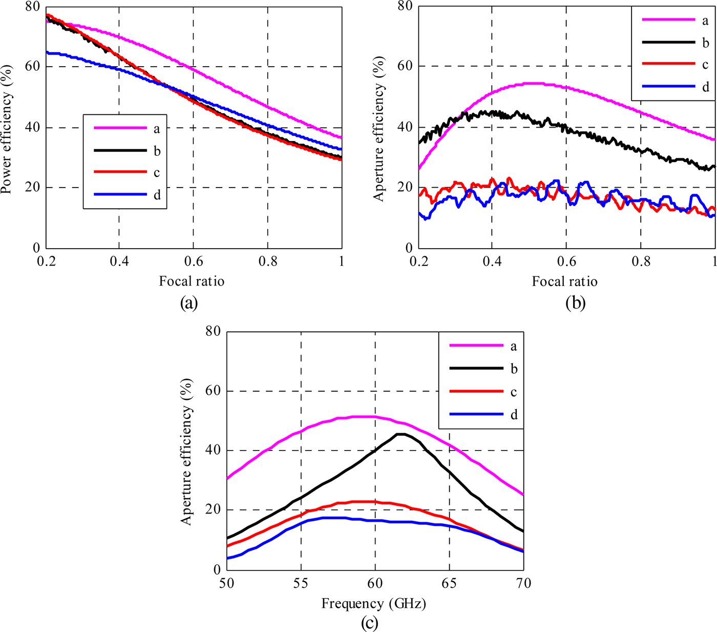
Fig. 11. In-house code simulation of the four lenses ‘a’, ‘b’, ‘c’, and ‘d’; (a) power efficiency at 60 GHz; (b) aperture efficiency versus focal ratio at 60 GHz; (c) aperture efficiency versus frequency for F/D = 0.4.
Nevertheless, the difference with other lenses remains below 10%, which indicates that the unit-cell losses of lenses ‘b’ and ‘c’ are very low.
Fig. 11(b) shows that the optimal focal ratio for ‘b’ and ‘c’ lenses is 0.4, while it is about 0.5 for lenses ‘a’ and ‘d’ which both are illuminated by a 10-dBi antenna of smaller beamwidth as compared with the planar focal source presented in Section III and chosen to reduce the thickness of the overall antenna. It can also be noted that the presence of the core dielectric layer does not affect significantly the aperture efficiency of the antenna since lenses ‘c’ and ‘d’ have very similar aperture efficiencies. Comparing lenses ‘b’ and ‘c’, we can attribute the 20% difference in aperture efficiency to the 3-bit and 1-bit phase quantization, respectively.
The aperture efficiency as a function of the frequency is given for a focal ratio of 0.4 in Fig. 11(c).
The half-maximum aperture-efficiency bandwidth of lenses ‘a’, ‘b’, ‘c’, and ‘d’ are 33, 20, 26, and 26%, respectively. The larger bandwidth of lens ‘a’ is expected as it is based on ideal unit cells of infinite transmission bandwidth and therefore the lens bandwidth is only limited by electrical path differences between the source and each unit cell. The lower bandwidth of lens ‘b’ can be explained by the lower bandwidth of via-less unit cells, in particular 0 and 45° unit cells as noted in Section II-B, even if a phase distribution containing the minimum number of these unit cells has been chosen. Lenses ‘c’ and ‘d’ are using the same unit cells and exhibit the same bandwidth, despite their different propagation medium between the focal source and the lens. This highlights that the core dielectric layer does not degrade significantly the lens bandwidth and the proposed architecture can be used for wideband applications.
In the following, lenses ‘b’ and ‘c’, based on via-less and rotated-patch unit cells, respectively, and using the core dielectric substrate are further investigated by comparing their performances using the in-house code and the full-wave simulations. The optimal focal ratio chosen for the two lenses is 0.4. The phase distributions corresponding to a maximum aperture efficiency for each discrete lens are shown in Figs 12(a) and 12(b) along with a view of the top layer.

Fig. 12. Discrete lens phase distribution (left) and top layer layout (right). (a) One-bit rotated-patch design (lens ‘c’), (b) 3-bit via-less design (lens ‘b’).
B) Simulation and experimental results
The fabricated prototype of lenses ‘c’ is shown in Fig. 13. The antennas have an effective diameter of 32 mm and a total thickness of 13.2 mm. The substrates and the ground planes were extended by 4 mm on each side in order to ease the assembly so that the total dimensions of the prototypes are 40 mm × 40 mm × 13.2 mm.
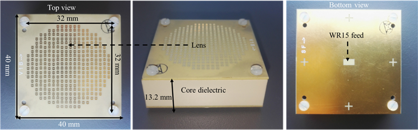
Fig. 13. Photos of the lens ‘c’ prototype.
The simulated and measured radiation patterns of lenses ‘b’ and ‘c’ are presented in Figs 14 and 15, respectively. Simulations are performed both using our in-house code and a full-wave Finite-Element Method simulator (Ansys HFSS). The radiation patterns are measured in an anechoic chamber in a standard far-field set-up. The rotated-patch discrete lens exhibits 17.6 dBi of measured gain at 60 GHz against 18.6 dBi in full-wave simulation, which corresponds to 14% aperture efficiency. The measured side-lobe levels are −20 dB in the H plane and −14 dB in the E plane. The measured cross-polarization levels in the broadside direction are below −30 dB. Thanks to the 3-bit phase quantization, the via-less discrete lens demonstrates a higher gain of 20.4 dBi in measurements at 61.5 GHz against 22.1 dBi in full-wave simulations, which corresponds to 26% aperture efficiency. The measured side-lobe levels are also lower (−23 dB in H plane and −18 dB in E plane). The measured cross-polarization levels in broadside direction are below −40 dB.
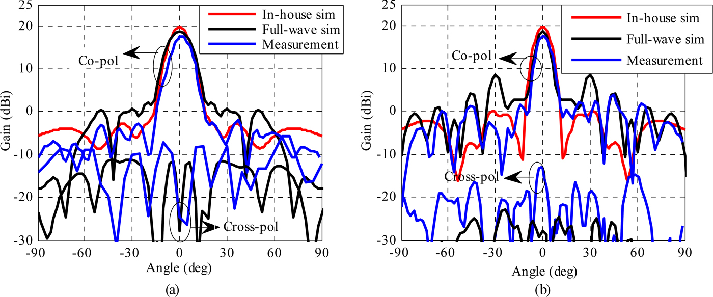
Fig. 14. Linearly polarized 1-bit rotated-patch discrete lens simulated radiation pattern at 60 GHz; (a) H plane, (b) E plane.
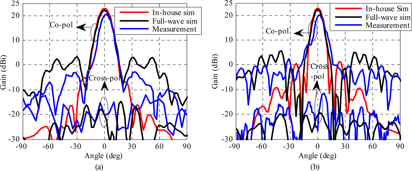
Fig. 15. Linearly polarized 3-bit via-less discrete lens simulated radiation pattern at 61.5 GHz; (a) H plane, (b) E plane.
A good agreement between simulated and measured radiation patterns is obtained at broadside angles with similar gain values and 3 dB beamwidths. For angles beyond 30° from the broadside direction, significant differences are noticed on the side-lobe levels between the full-wave simulations and the in-house code simulations; these differences are mostly attributed to spillover radiations that are not taken into account in the in-house code and represents 35% (−1.9 dB) of the power radiated by the focal source. In contrast to discrete lenses fed through air, the thick dielectric layer between the focal source and the discrete lens introduces a dielectric–air interface at the edges which generates some residual reflection and refraction of the spillover radiation toward angles larger than 30°. Figures 16(a) and 16(b) showing the electric field distribution in and around the antenna suggest that these effects are small, although they cannot be easily quantified. Figure 16(c) shows the phase of the E field at 61.5 GHz in the horizontal plane at half a wavelength above lens ‘c’ (as an example) where a quasi-constant phase is observed on most of the aperture.

Fig. 16. Electric field distribution at 61.5 GHz for lens ‘c’: (a) magnitude in E plane and (b) H plane; (c) phase in an horizontal (XY) plane half-wavelength above the discrete lens.
Other causes of discrepancy between simulations and measurements include the assumptions of normal incidence and perfect periodicity in unit-cells simulations, the limited accuracy of full-wave simulations for antennas of such large electrical size due to limited computer resources and simulation time, and fabrication tolerances, in particular with possible air gaps on both sides of the core dielectric substrate.
The simulated and measured reflection coefficient of the rotated patch and via-less discrete lenses exhibit a good agreement (Fig. 17(a)). The measured reflection coefficients are below −10 dB over the 50–68 GHz band and are similar to the one of the focal source alone ‘without lens’ observed in Fig. 3(b).
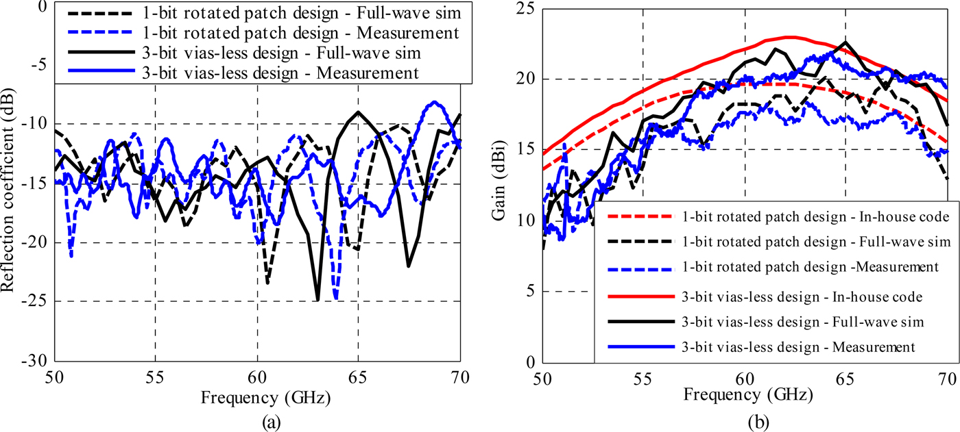
Fig. 17. One-bit rotated-patch and 3-bit via-less discrete-lenses frequency responses. (a) Reflection coefficient, (b) gain.
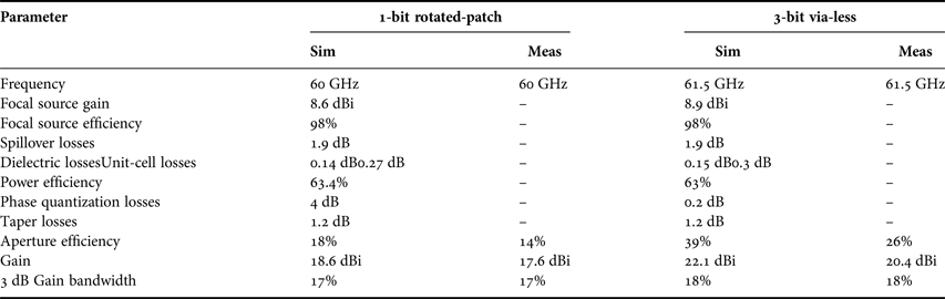
The gain-frequency response of both lenses is presented in Fig. 17(b). A good agreement (~1 dB difference) between full-wave simulations and measurements is observed for both antenna prototypes, while the in-house code slightly overestimates gain levels. Over the 57–66 GHz band, the errors between the two simulations amount to 2.4 dB maximum, as well as between full-wave simulation and measurement. The 3 dB measured fractional-gain bandwidths are 17 and 18% for the rotated-patch and the via-less lenses, respectively. For the former lens, the bandwidth is quite close to the result (19%) reported earlier from the in-house code simulation, while it is slightly lower for the latter lens (26% in the in-house code simulation). These bandwidth values are significantly lower than those simulated for the unit cells in Section II, which shows that the bandwidth of these antennas is primarily limited by the chosen focal ratio. Nevertheless, these performances in terms of bandwidth and gain are expected to be suitable for many short-range wireless applications. Scaling the structure to larger apertures should allow to reach higher gain values provided an appropriate focal source is designed to illuminate the aperture efficiently, which usually requires a larger focal distance and therefore a thicker core dielectric layer. The power budget presented further indicates that the core dielectric layer losses are low and its thickness could be significantly increased before strongly degrading the overall efficiency; for instance, 1 dB of dielectric losses at 60 GHz is estimated to correspond to a dielectric thickness of about 86 mm and a lens of about 250 mm diameter (with F/D ~ 0.35) and 39 dBi gain (~30% aperture efficiency).
The power budget of both lenses is presented in Table 5. It is clear that the main difference between them is the phase quantization error (4 dB for the 1-bit lens against 0.2 dB for the 3-bit lens). The low-phase quantization losses of the 3-bit lens (0.2 dB) shows that a unit cell offering a finer phase quantization would only slightly improve the antenna efficiency at the risk of a more complex design. Except from phase quantization, the main losses are associated to the spill-over radiation and illumination taper, which are mostly dependent on the focal source. These losses are comparable to classical discrete lenses (without core substrate) with the same focal distances and fed by horn antennas [Reference Kaouach, Dussopt, Lantéri, Koleck and Sauleau28]. The addition of the core substrate does not affect the power budget as the added dielectric losses are very low (0.15 dB) and makes this topology suitable for highly integrated and efficient millimeter-wave antennas. As discussed in Section III, the unit-cell losses are low (~0.3 dB) for both unit cells and comparable to those of similar structures designed in air in this frequency band.
Table 5. Power budget of the 1-bit rotated-patch and 3-bit via-less discrete lenses.

VI. CONCLUSION
A new topology of low-cost high-gain integrated antenna compatible with millimeter-wave transceivers integration is introduced. It consists in a planar discrete lens and a planar focal source printed on both sides of a core dielectric substrate. Two linearly polarized discrete lenses based on the proposed architecture have been designed using rotated-patch and via-less unit cells. The design rules and performance of each antenna element are discussed and attractive experimental radiation performances are presented in V-band with 14–26% aperture efficiency and 17–18% 3 dB fractional-gain bandwidth for 1-bit and 3-bit designs, respectively. It is shown that the core substrate does not degrade significantly the radiation performances but improves compactness (0.4 focal ratio, 13.2 mm thickness), eases alignment and positioning of elements constituting the antenna, and is compatible with standard planar technologies and pave the way to cost-effective, efficient, and robust discrete lens at higher frequencies in a standard and monolithic planar technology.
APPENDIX A
A.1 Core Dielectric Characterization
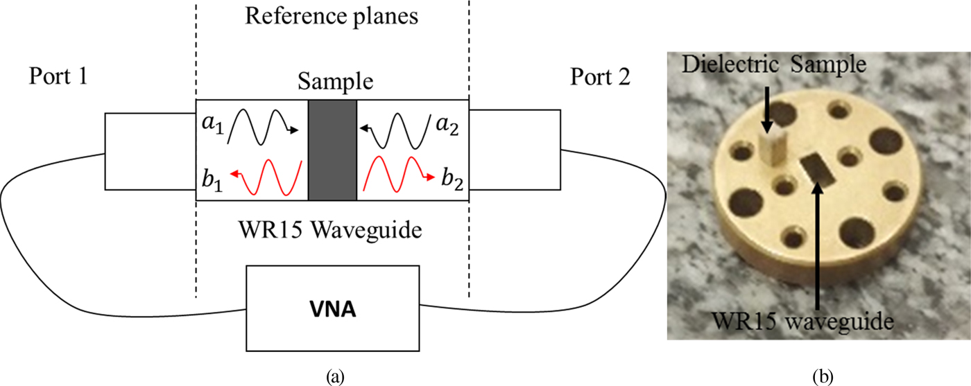
Five materials have been characterized in V-band: polycarbonate (PC), acrylonitrile butadiene styrene (ABS), polybenzimidazole (PBI), polyether ether ketone (PEEK), and polyphenylene sulphide (PPS). Material samples were machined to fit in a standard WR15 rectangular waveguide (3.76 mm × 1.88 mm section) with different thicknesses ranging from 0.5 to 1.5 λ g. Two-port S-parameter measurements were performed using a standard vector network analyzer and a short-open-load-thru calibration at the interface plane of the sample holder (Fig. 18). Multiple samples have been measured for each material to mitigate the uncertainties on samples dimensions and positioning in the holder [Reference Chen, Ong, Neo, Varadan and Varadan33].

Fig. 18. Plastic material (a) characterization setup and (b) WR15 sample holder.
The measurements were fitted to full-wave electromagnetic simulations in order to extract the dielectric characteristics of each material, which are assumed to be constant over the V-band. As shown in Figs 19(a) to 19(d), a good agreement in both magnitude and phase is obtained between measurements and simulations.

Fig. 19. Simulated (solid line) and experimental (dashed lines) S parameters of the dielectric material samples: reflection coefficient (a) magnitude and (c) phase; transmission coefficient (b) magnitude and (d) phase.
A.2 Ideal Unit Cells Model
The ideal unit cells used in the in-house code is a rectangular aperture on infinite ground plane with normalized radiation pattern equations defined as follow [Reference Balanis34]:
 $$H_\theta (\theta, \varphi ) = \displaystyle{{\cos (\theta )\cos (\varphi )(\sin (X))(\sin (Y))} \over {XY}}\;,$$
 $$H_\varphi (\theta, \varphi ) = \displaystyle{{{\rm sin}(\varphi )(\sin (X))(\sin (Y))} \over {XY}}\;,$$
where:
 $$X = \displaystyle{{\pi a} \over {\lambda _g}}\sin (\theta ){\rm cos}(\varphi ),\rpar$$
 $$Y = \displaystyle{{\pi b} \over {\lambda _g}}\sin (\theta ){\rm sin}(\varphi ).$$
And H is the normalized antenna radiation pattern, the guided wavelength, and a and b the length and width of the aperture. The directivity D 0 of the λ g aperture is defined as
 $$D_0 = \displaystyle{{4\pi ab} \over {\lambda _g^2}}.$$
For the presented case (a = b = 1.6 mm, εr = 3, tanδ = 0.001), D 0 is equal to 5.9 dBi.
 Kossaila Medrar received the B.S. degree in Electrical Engineering from the Ecole Nationale Supérieure De Technologie of Algiers, Algeria, and M.S. degree in Electronical Engineering for Communication Systems from the University of Bretagne Occidentale, France in 2013 and 2015, respectively. He is currently working toward the Ph.D. degree in Optical and Radiofrequency Engineering at CEA-LETI, France and University of Grenoble Alpes, France. His research interests include antenna arrays, frequency selective surfaces, quasi-optical antennas, and high gain antennas at millimeter wave frequencies.
 Loic Marnat received his M.S. and Ph.D. degrees in Electrical Engineering at the Institut National des Sciences Appliqués (INSA) de Rennes, France, in 2006 and 2009, respectively. He started as a Lecturer and Research Fellow at the INSA de Rennes in 2010. From 2010 to 2013, he was a postdoctoral fellow at the King Abdullah University of Science and Technology (KAUST) in Saudi Arabia. Since 2014, he has been a research engineer and project leader in integrated antenna systems at CEA-LETI in France. His research interests are in highly integrated antenna systems and advanced packaging technique for efficient and reconfigurable front-ends.
 Laurent Dussopt received the Ph.D. degree in Electrical Engineering from the University of Nice-Sophia Antipolis, France, in 2000, and the “Habilitation à Diriger des Recherches” degree from the University of Grenoble, France, in 2008. From 2000 to 2002, he was a Research Fellow with the University of Michigan. Since 2003, he has been with CEA-LETI, as a Research Engineer and Project Leader on advanced antenna systems for millimeter-wave wireless communications at microwave and frequencies. He was elevated to the grade of research director of CEA in 2015. Since 2016, he is a project leader on THz imaging systems in the Optics and Photonics division of CEA-LETI. Dr. Dussopt has published more than 200 scientific papers in international journals and conferences, eight book chapters and several patents; he contributes to the technical program committees of several international conferences and the IEEE MTT-20 Technical Committee on wireless communications.