I. INTRODUCTION
The substrate-integrated waveguide (SIW) technology combines the advantages of the conventional metallic waveguide and the planar circuit. Thus, they have a high-quality factor, low insertion loss, high integration ability, and low fabrication cost. Hence, it is considered as an important technology to design a high-performance circuit [Reference Castellano1–Reference Tseng and Chu6]. The basic geometry of the SIW circuit consists of a network of metallic cylinders that are embedded in a dielectric substrate layer. These cylinders constitute a lateral discrete metallic as in the case of conventional waveguide.
The analytical study of SIW circuits is solved by empirical formulas of effective physical dimensions [Reference Tseng and Chu6–Reference Deslandes and Wu8]. All these formulas are restricted in the simple structures and canonical forms such as the waveguide transition. In the case of arbitrary configurations, these expressions are invalid. Hence, the use of a rigorous numerical method is necessary. Several methods are proposed in the literature, which can accurately predict the electromagnetic behavior of SIW devices such as the frequency domain finite differences method, the finite-elements method (FEM) [Reference Ettorre, Sauleau and Le Coq9, Reference Ettorre, Neto, Gerini and Maci10], the moments of method [Reference Valerio, Casaletti, Seljan, Ettorre and Sauleau11–Reference Arnieri and Amendola13], and semi-analytical method based on the Green Function [Reference Amendola, Arnieri and Boccia12]. The memory usage and the computational time requirements of these methods do not allow the investigation of a wide range of applications which have large size or complex geometry or high number of metallic via-holes.
In this paper, we propose a new approach using the iterative method for a rigorous study of the SIW structures. The iterative method is based on the wave concept [Reference Hrizi and Sboui14–Reference Sboui, Gharsallah, Gharbi and Baudrand16]. The iterative method is already improved for modeling the planar circuits, and it is validated in the multi-layer structures and in periodic problems [Reference Hrizi and Sboui14]. This method does not require the treatment of boundary conditions on the truncated computational domains. The relation of field-current is converted to a relation of incidental-reflected waves. The reflexion operator of the waves has an amplitude less than the unit. Therefore, the convergence of this method is guaranteed. The principle of the iterative method is based on the recurrent relation of the transverse incident-reflected waves between the spatial and the spectral domains. The spatial domain is used to satisfy the boundary conditions on the circuit plane. This domain is modeled by a spatial operator, noted S Ω. The spectral domain is used to calculate the propagation in the medium (air or dielectric). This domain is modeled by a modal operator, noted Γ. We can better understand the iterative method in [Reference Sboui, Gharsallah, Baudrand and Gharbi17–Reference Guclu, Campione and Capolino19].
The iterative method is adapted to homogenous planar circuit using the transverse waves (at discontinuity interfaces). Therefore, this method is unable to study the SIW devices, which have a network of metallic via-holes embedded in the dielectric layer. In fact, the transverse waves did not permit to take into account the boundary condition of vertical metallic via-hole. In this paper, we develop a new formulation of the iterative method for the analysis SIW circuits, using the concept of the longitudinal waves, which are parallel to the metallic via-holes.
The basic idea consists in analyzing the SIW circuits as two-dimensional (2D)-periodic structure with defects. In the spectral domain; we assume that the structure is 2D-periodic without defects using the Floquet–Bloch transformation. Therefore, we limit the study to a single cell. Then, in the spatial domain, the boundary conditions, and the continuity equation are satisfied at each cell. The new approach is described in both spectral and spatial domains. We note that in this work we study the case when all metallic via-holes have the same diameter and their height is equal to the thickness of the substrate.
The first section presents the theoretical development of the SIW structures using the modal approach and the Floquet–Bloch Theorem. The second section presents the formulation of the problem using concept of longitudinal waves. We determined the expressions of the electric field and current, and the diffraction matrix [S]. In the third part, the computational complexity of the present approach is discussed. Finally, to valid this approach, two different structures are analyzed. The first is a substrate-integrated cavity and the second is a substrate-integrated waveguide quasi-elliptic filter for V-band. Transmission and the reflection coefficients are compared with measurements data and with HFSS software (the FEM method) simulations; then we evaluate the performance of the new method by comparing the error and the computation CPU time with HFSS simulations.
II. THEORY
The basic schematic of the SIW circuit, presented in Fig. 1 is composed by a dielectric substrate placed between two parallel metal planes (top and bottom), and it contains rows or a network of metallic via-holes.

Fig. 1. SIW geometry.
Considering the planar architecture of the SIW structure, there are two groups of modes: transverse magnetic (TM) with the components (E z , Hx , and H y ) and transverse electric (TE) with the components (H z , Ex , and E y ); (where (E x , Ey, Ez ) and (H x , Hy , and H z ) are, respectively, the components of the electric and magnetic fields). Additionally, the lateral metallic walls (discrete) formed by the metallic via-holes network stop the propagation of modes having the current lines which are perpendicular to the metallic via-holes (E x , Ey ). Thereafter, only TM modes satisfy the boundary conditions [Reference Castellano1, Reference Xu and Wu7], and then the electric fields admit only the one component E z . Consequently, the boundary conditions on the top and bottom metal planes are automatically guarantees and we analyze the boundaries conditions related to the metallic via holes.
A) Spatial operator
In the propagation medium (dielectric layer), the metallic via-hole is directed along the z-direction. We define the incident A z and reflected B z waves as a linear combination of electric field E z and the current density vector J z , (1).
 $$\left\{ {\matrix{ {{A_z} = \displaystyle{1 \over {2\sqrt {{z_0}}}} \left( {{E_z} + {z_0}{J_z}} \right),} \cr {{B_z} = \displaystyle{1 \over {2\sqrt {{z_0}}}} \left( {{E_z} - {z_0}{J_z}} \right),} \cr}} \right.$$
where z 0 is the characteristic impedance of the medium.
The discretization process for a SIW cavity example is illustrated in Fig. 2, we distingue the three sub-domains: sources cells, metallic via-hole cell, and without-metallic-via-hole cell, where H δ are their projections matrices, are defined as follows:
 $$\eqalign{{\left[ {{H_\delta}} \right]_{{N_x},{N_y}}} & = \left\{ {\matrix{ 1 & {\hbox{on the sub-domain }\! "\delta\," } \cr {\rm 0} & {{\rm elsewhere}} \cr}} \right.;\quad \cr \delta & = \left\{ {\matrix{ s & {\hbox{ for the source sub-domain,}} \cr v & {\hbox{for the metallic via-hole sub-domain,}} \cr {nv} & {\hbox {for the without-via-hole sub-domain,}} \cr}} \right.} $$
where N x is the number of cells according to the x-direction, and N y is the number of cells according to the y-direction.

Fig. 2. Discretization of the spatial domain of a substrate-integrated cavity.
The boundary conditions for each point of the structure are presented by a spatial coefficient.
The spatial operator Ω is used to calculate the reflected waves from the incident waves in the spatial domain, as in (2). Its calculation requires the application of the appropriate boundary conditions.
 $${A_z}\left( {i,j} \right) = \left[ {\Omega \left( {i,j} \right)} \right]{\rm} {B_z}\left( {i,j} \right) + {A_0},$$
where (i, j) are the coordinates of the cell (in the total structure) according to the x-direction and y-direction and A 0 is the excitation defined on the source domain. The boundary conditions in the all sub-domains are is defined in the following equations (3)
 $$\left\{ {\matrix{ {\hbox{On the sub-domain}} & {{H_v}{\rm :} \left\{ {\matrix{ {{E_z} = 0,} \cr {{J_z} \ne 0,} \cr}} \right.} \cr {\hbox{On the sub-domain}} & {{H_{nv}}{\rm :} \left\{ {\matrix{ {{E_z} \ne 0,} \cr {{J_z} = 0,} \cr}} \right.} \cr {\hbox{On the sub-domain}} & {{H_s}{\rm :} \left\{ {\matrix{ {{E_z} = {E_0},} \cr {{J_z} = {J_0} = \displaystyle{{{E_0}} \over {{z_0}}},} \cr}} \right.} \cr}} \right.$$
where E 0 is the excitation source of the circuit.
The use of (1) and (3), allows one to establish the relationship between the incidents and reflected waves, as in (4).
 $$\left\{ {\matrix{ {{H_v} \Rightarrow A_z^{k + 1} = - B_z^k ,} \hfill \cr {{H_{nv}} \Rightarrow A_z^{k + 1} = B_z^k ,} \hfill \cr {{H_s} \Rightarrow A_z^{k + 1} = 0 \cdot B_z^{k + 1} + {A_0},} \cr } } \right. $$
where “k” is the iteration number.
The general expression for the spatial operator Ω is given by (5):
 $$\Omega = 0.{H_s} + {H_{nv}} - {H_v}.$$
B) Spectral study
The medium is modeled by a spectral operator, which permit to take into account of the scattering behavior. This operator permits to calculate the reflected waves from the incident waves in the spectral domain, as in (6), [Reference Hrizi and Sboui14].
 $$\left[ {\tilde B} \right] = \left[ \Gamma \right] \cdot \left[ {\tilde A} \right].$$
The connection between the spatial domain and the spectral domain is ensured by a fast transformation in mode using the bi-dimensional fast Fourier transform 2D-FFT and its inverse transform.
 $$\left \vert {\matrix{ {\tilde A} \cr {\tilde B} \cr}} \right \vert = FMT\left \vert {\matrix{ A \cr B \cr}} \right \vert. $$
In order to solve the scattering problem, we assume that the structure is 2D-periodic. We consider a bi-periodic array in SIW structure, as depicted in Fig. 3(a). The dimensions of the structure according to O x and O y are D x and D y . The periods according to O x and O y are d x and d y . The effective domain of the metal in the basic cell is d 0, as illustrated in Fig. 3(b). The height of the dielectric layer is h.

Fig. 3. The cross-section of the bi-periodic SIW schema in case of square metallic via-hole (a) and the configuration of the basic cell (b).
The spectral impedance is obtained from the Helmholtz equation is given by (7), where Δ T is the transverse Laplace operator
 $$\left( {{\Delta _T} + {k^2}} \right){E_z} = j\omega \mu {J_z}, $$
where E is the electric field and
 $J = H \times \vec n$
is the current density vector, and
$J = H \times \vec n$
is the current density vector, and
 $\vec n$
is the normal vector.
$\vec n$
is the normal vector.
We consider the modal basis functions given by (8), deduced from the Floquet–Bloch theorem as in [Reference Hamdi, Aguili and Baudrand18–Reference Islam, Zedler and Eleftheriades20].
 $$\eqalign{\left \vert {f{}_{pq,mn}} \right\rangle & = {a_{pq,mn}}.\exp \left( {j\left( {{\alpha _p}x + {\beta _q}y} \right)} \right) \cr & \quad \times\exp \left( {j\left( {\displaystyle{{2\pi m} \over {{d_x}}}x + \displaystyle{{2\pi n} \over {{d_y}}}y} \right)} \right) = {f_{pq}}{f_{mn}},} $$
where
 ${\alpha _p} = 2\pi p/{D_x}$
,
${\alpha _p} = 2\pi p/{D_x}$
,
 ${\beta _q} = 2\pi q/{D_y}$
are the Floquet–Bloch states, and
${\beta _q} = 2\pi q/{D_y}$
are the Floquet–Bloch states, and
 ${a_{pq,mn}} = \left\langle {{f{}_{pq,mn}}} \mathrel{\left\vert {\vphantom {{f{}_{pq,mn}} {f{}_{pq,mn}}}} \right.} {{f{}_{pq,mn}}} \right\rangle $
are the amplitude of the mode f
pq,mn
.
${a_{pq,mn}} = \left\langle {{f{}_{pq,mn}}} \mathrel{\left\vert {\vphantom {{f{}_{pq,mn}} {f{}_{pq,mn}}}} \right.} {{f{}_{pq,mn}}} \right\rangle $
are the amplitude of the mode f
pq,mn
.
The electric field vector and the current density, using the global modal basis functions (Floquet–Bloch states), are given by (9)
 $$\eqalign{E & = \sum\limits_{pq} {\left \vert {{f_{pq}}} \right\rangle {{\tilde E}_{pq}}\left\langle {{f_{pq}}} \right \vert}\, \;{\rm and\;} \; J = \sum\limits_{pq} {\left \vert {{f_{pq}}} \right\rangle {{\tilde J}_{pq}}\left\langle {{f_{pq}}} \right \vert},} $$
The structure is centered at the origin of the coordinate system (the basic cell is located in the center of the structure). So
 $ - {N_x}/2 \le p \le {N_x}/2 - 1$
and
$ - {N_x}/2 \le p \le {N_x}/2 - 1$
and
 $ - {N_y}/2 \le q \le {N_y}/2 - 1.$
We can write the operator Δ T in the modal basis f pq,mn as in (7).
 $${\Delta _T}f{}_{pq,mn} = - {\left( {{\alpha _p} + \displaystyle{{2\pi m} \over {{d_x}}}{\rm}} \right)^2} - {\left( {{\beta _q} + \displaystyle{{2\pi n} \over {{d_y}}}} \right)^{\rm 2}}{\rm} {\rm.} $$
The current density is equal to zero in the dielectric area. Thus electric field vector and the current density on metal sub-domain are given by (11):
 $${E_{pq}} = \left\langle {{{{\tilde E}_{pq}}}} \mathrel{\left \vert {\vphantom {{{{\tilde E}_{pq}}} {{h_m}}}} \right.} {{{h_m}}} \right\rangle ;\quad {\rm} {J_{pq}} = \left\langle {{{{\tilde J}_{pq}}}} \mathrel{\left \vert {\vphantom {{{{\tilde J}_{pq}}} {{h_m}}}} \right.} {{{h_m}}} \right\rangle, $$
where h m is the effective domain of the metal sub-domain in the basic cell, as illustrated by Fig. 3(b), given by:
 $${h_m} = \left\{ {\matrix{ {\matrix{ 1 & {{\rm si} \left( {x,y} \right) \in \left[ { - \displaystyle{{{{\rm d}_{\rm 0}}} \over {\rm 2}},\displaystyle{{{d_0}} \over 2}} \right] \times {\rm} \left[ { - \displaystyle{{{{\rm d}_{\rm 0}}} \over {\rm 2}},\displaystyle{{{d_0}} \over 2}} \right]} \cr 0 & {{\rm elsewhere}{\rm.}} \cr} {\rm,}} \hfill \cr {{\rm}} \hfill \cr}} \right.$$
The spectral impedance z pq connects the components J pq and E pq as in (12):
 $${E_{pq}} = z{}_{pq} \cdot {J_{pq}}.$$
We can write the impedance operator using the modal base
 $\left\langle {{f_{pq}}} \right\vert$
as in (13).
$\left\langle {{f_{pq}}} \right\vert$
as in (13).
 $$z = \sum\limits_{p,q} {\left \vert {{f_{pq}}} \right\rangle {z_{pq}}\left\langle {{f_{pq}}} \right \vert} {\rm} {\rm.} $$
To take into account the configuration of the basic cell we can decompose the impedance operator on the local modal base:
 $\left\langle {{f_{pq}}{f_{mn}}} \right\vert$
, as in (14).
$\left\langle {{f_{pq}}{f_{mn}}} \right\vert$
, as in (14).
 $${z_{pq}} = \sum\limits_{m,n} {\left \vert {{f_{pq}}{f_{mn}}} \right\rangle {z_{pq,mn}}\left\langle {{f_{pq}}{f_{mn}}} \right \vert} {\rm} {\rm.} $$
Coupling (7–10–12–14); the impedance operator z pq is given by (15).
 $${z_{pq}} = \sum\limits_{m,n} {\left\langle {{{H_m}}} \mathrel{\left \vert {\vphantom {{{H_m}} {{f_{pq}}{f_{mn}}}}} \right.} {{{f_{pq}}{f_{mn}}}} \right\rangle} {\rm} j\omega \mu \displaystyle{1 \over {{k^2} - \alpha _{p,m}^2 - \beta _{q,n}^2}} \left\langle {{{f_{pq}}{f_{mn}}}} \mathrel{\left \vert {\vphantom {{{f_{pq}}{f_{mn}}} {{H_m}}}} \right.} {{{H_m}}} \right\rangle, $$
where
 ${\alpha _{p,m}} = {\alpha _p} + (2\pi m/{d_x})$
and
${\alpha _{p,m}} = {\alpha _p} + (2\pi m/{d_x})$
and
 ${\beta _{q,n}} = {\beta _q} + (2\pi n/{d_y}){\rm } {\rm.} $
The final expression of the spectral impedance is given by (16)
${\beta _{q,n}} = {\beta _q} + (2\pi n/{d_y}){\rm } {\rm.} $
The final expression of the spectral impedance is given by (16)
 $${z_{pq}} = \sum\limits_{mn} {j\omega \mu \displaystyle{{{{\left \vert {\left\langle {{H_m}{f_{pq}}{f_{mn}}} \right\rangle} \right \vert} ^2}} \over {{k^2} - \alpha _{p,m}^2 - \beta _{q,n}^2}}} {\rm,} $$
where
 ${H_m} = (1/\sqrt s ){h_m}$
and S is the cross-section of metallic via-hole
${H_m} = (1/\sqrt s ){h_m}$
and S is the cross-section of metallic via-hole
The propagation constant is given by the following expression:
 ${\gamma_{pq}} = \sqrt {( {{k^2} - \alpha_{p,m}^2 - \beta_{q,n}^2})}$
In the case of shorted-circuited structure with a ground plane at a height h, the spectral operator Γ
pq
is given by (17).
${\gamma_{pq}} = \sqrt {( {{k^2} - \alpha_{p,m}^2 - \beta_{q,n}^2})}$
In the case of shorted-circuited structure with a ground plane at a height h, the spectral operator Γ
pq
is given by (17).
 $${\Gamma _{pq}} = \displaystyle{{{z_0} - {z_{pq}}\coth \big( {{\gamma _{pq}}h} \big)} \over {{z_0} + {z_{pq}}\coth \big ( {{\gamma _{pq}}h} \big)}}{\rm} {\rm.} $$
After the convergence value-iteration of the iterative process, the output parameters are extracted. The distribution of the electric field and the current is given by (18).
 $$\eqalign{& {E_z}\left( {i,j} \right) = \sqrt {{Z_0}} \left( {{A_z}\left( {i,j} \right) + {B_z}\left( {i,j} \right)} \right){\rm ;} \cr & {\rm} {J_z}\left( {i,j} \right) = \displaystyle{1 \over {\sqrt {{Z_0}}}} \left( {{A_z}\left( {i,j} \right) - {B_z}\left( {i,j} \right)} \right).} $$
The matrix S of the studied structure is given by (19).
 $$\left[ S \right] = \displaystyle{{\left[ {{I_d}} \right] - {z_0}\left[ Y \right]} \over {\left[ {{I_d}} \right] - {z_0}\left[ Y \right]}},$$
where I d is the identity matrix and Y is the admittance matrix of circuit.
III. APPLICATIONS
The developed approach is used to study tow SIW circuits (for both loss and lossless cases). The first is a substrate-integrated cavity and the second is a quasi-elliptic filter in the V-band.
A) Integrated substrate cavity
The structure presented in Fig. 4 is a single substrate-integrated cavity first presented in [Reference Amendola, Arnieri and Boccia12], the lateral walls are realized by rows of metallic via-holes. The used substrate is Arlon 25FR (tm) with dielectric constant of 3.58 and thickness of 0.787 mm. The total structure dimensions are 15.17 × 24 mm2. The metallic via-holes have the same diameter d 0 = 0.2 mm and with a period p = 2 mm.

Fig. 4. SIW cavity.
To verify the stability of the proposed approach, we have performed a study of the convergence behavior of iterations and of the number of modal bases (m,n). Figure 5 illustrate the convergence curves value- iterations of the reflection and transmission coefficients taken at a frequency equal to 10 GHz. The convergence is reached around 200 iterations (with a ripple rate of 10−3).

Fig. 5. Convergence curves value-iterations of S-parameters (Frequency = 10 GHz; Number of iterations = 250 iterations).
On the other hand, the developed approach is based on the superposition of infinite series of modes. Considering, the limitation of the computational resources which increase considerably with this number, it is necessary to stop this series at a finite number of modes (M,N). In this part, we studied the convergence as function of the number of modes (M,N). The curves in Fig. 6(a) present the reflexion coefficient (S11) for different numbers (M,N).

Fig. 6. (a) Reflection coefficient for different number of the modes (M,N). (b) Convergence curve of the resonance frequency depending of the number of modes (M,N).
Figure 6(b) represents the convergence curve of the resonant frequency of the cavity versus (M,N). The convergence value-modes achieved around 30 modes. Therefore, it is unnecessary to take a number of modes higher than 30.
The convergence value-iterations and value-modes show that the proposed method is numerically stable.
Using the same example of the SIW cavity, depicted in the Fig. 4, we study the effect of the diameter of the metallic via-hole on the frequency response. Figure 7(a) depicts the reflection coefficient of different values of the diameter d 0. Figure 7(b) presents the behavior of the resonance frequency depending on the diameter of metallic via-hole. The increase of the diameter has effect to decrease the resonance frequency of the cavity.

Fig. 7. (a) Effect of the diameter of the metallic via-hole. (b) Resonance frequency versus the via-hole diameter.
The results obtained are compared with both measurements that are available in [Reference Amendola, Arnieri and Boccia12] and with data obtained by the FEM (commercial software HFSS). Figures 8(a) and 8(b) display the transmission and reflection coefficients for the frequency range 8–10 GHz. A satisfactory agreement is observed. This allows validating the accuracy of the present method. Moreover, the HFSS software present a frequency shift of 55 MHz, this shift is close to zero for our method.

Fig. 8. (a) Reflection coefficient S11 versus frequency. (b) Transmission coefficient S21 versus frequency.
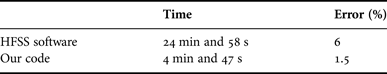
All simulations are carried out using a CPU Intel (R) Core (TM) i5 CPU 650@3.20 GHz with a RAM equal to 6 GB. The error and the computation CPU time are recorded in Table 1. The proposed method has the most precise results and the average error does not exceed 2%. Also, the proposed method allows a reduction of the computing time of more than 80%. In fact, the HFSS software becomes very slow if we introduce the metallic via-holes.
Table 1. Computation performance comparison of the proposed method and the FEM method for the SIW cavity example.

B) Quasi-elliptic V-band filter
The structure showed in Fig. 9 is a quasi-elliptic filter [Reference Zelenchuk and Fusco21].This circuit is used in high-speed wireless system, in the V-band, with 9 GHz bandwidth. In [Reference Guglielmi, Jarry, Kerherver, Roquebrun and Schmitt22], the multi-mode cavity filter techniques are used to design this circuit. The via-holes have the dimension of d 0 = 0.25 mm and spaced of 0.4 mm and the other dimensions of the filter are:
 $$\eqalign{{b_1} & = 2.55\;{\rm mm},{b_2} = 1.56\,{\rm mm},\;{b_3} = 6.32\,{\rm mm},\;{b_4} = 1.71\,{\rm mm}, \cr & \quad {b_5} = 2.11\,{\rm mm},\;{b_6} = 6.71\,{\rm mm,}\;{b_7} = 2.25\,{\rm mm}, \cr {a_1} & = 1.84\,{\rm mm},\;{a_2} = 1.84\,{\rm mm},\;{a_3} = 1.65\,{\rm mm},\;{a_4} = 2.5\,{\rm mm}, \cr & \quad {a_5} = 1.12\,{\rm mm},\;{\varepsilon _r} = 2.1,\;h = 0.2\,{\rm mm}{\rm.}} $$

Fig. 9. Top view of the SIW quasi-elliptic filter.
Figures 10(a) and 10(b) present the reflection and transmission coefficients obtained by both the proposed method and by the commercial software HFSS, and compared with the measurement data available in [Reference Zelenchuk and Fusco21]. A satisfactory agreement is observed.

Fig. 10. (a) Reflection coefficient of the SIW quasi-elliptic filter. (b) Transmission coefficient of the SIW quasi-elliptic filter.
IV. CONCLUSION
This paper presents a new formulation of iterative method used to analyze single-layer SIW circuit. The convergence study allows saving the CPU time and the memory space without sacrificing accuracy. The obtained results are validated by the commercial software HFSS simulations and measurements data available in the literature which prove the accuracy of the method. The proposed method is recommended for the efficient analysis of SIW structures having big sizes.
ACKNOWLEDGEMENTS
This work was supported by the Laboratory of Physics of soft matter and electromagnetic modeling, Faculty of Sciences of Tunis, Campus University 2092; Tunis, Tunisia. The authors are also truly grateful to the unanimous reviewers and Associate Editor for their critical comments and suggestions to improve the quality of the manuscript.
 Ben Romdhan Hajri Jamel received the Master degrees in Electronic Systems from the Faculté des sciences de Tunis in 2011. Currently, he is working toward his Ph.D. His research interests are the numerical method for electromagnetic modeling.
 Hrizi Hafedh is a Doctorate of Electronic. Since 2011 he has been with Institut Supérieur d'Informatique et des Techniques de Communication Hammam Sousse. His current research interests include the modeling of microwave circuits.
 Sboui Noureddine is a Professor of Electrical Engineering. Since 2002 he has been with the Faculté des Sciences de Tunis. His current research interest includes the areas of numerical methods, electromagnetic field problems, and advanced microwave circuits and components.