


I. INTRODUCTION
RF MEMS switches are a topic of active research since the early 1990s. They show some very attractive properties like low insertion loss, negligible DC-power consumption, and very high linearity, which make them a promising candidate to replace conventional technologies like PIN diodes or field effect transistor (FET) transistors in certain applications or to enable completely new devices and functionalities.
Some outstanding examples out of a large number of research institutes and companies, which are dedicated to developing RF MEMS switching concepts and products, are Radant [1], MEMtronics [2], Raytheon [Reference Pillans3], MIT Lincoln Labs [Reference Muldavin, Bozler, Rabe, Wyatt and Keast4], Advantest [5], OMRON [Reference Seki6], XCOMwireless [7], WiSpry [8], TDK-EPC [9], LETI [Reference Robert10], and NXP [Reference Wunnicke11].
RF MEMS switch technologies, however, suffered for a long time from reliability issues and still do, even though there are now a few examples of RF MEMS switch products that are available for purchase. In addition, due to their potential use in military applications, they are or might become subject to international trade in arms regulations.
At EADS, being a company in the field of aeronautics and space, there are a number of potential applications that would benefit from the availability of proper RF MEMS switch devices. First and foremost, there are electronically steerable antennas which are or could be used for numerous different purposes like situation awareness in helicopters, wake vortex detection in passenger airplanes, or body scanners at security checkpoints. RF MEMS switches could replace the circulator in transmit/receive modules and improve the isolation between signal paths as well as make the modules smaller. Electronic warfare could make use of RF MEMS-tunable filters, antennas, and multiband amplifiers. The same is true for space systems, where RF MEMS switches would also be implemented as redundancy switches and in switch matrices for communication satellites. A number of other potential applications are there as well, especially where a combination of low insertion loss, high-frequency, low DC-power consumption, high RF-power handling, or high linearity is needed.
For these reasons, EADS launched its own RF MEMS switch research program in 2003. The focus of this activity is – opposed to many other efforts – a concept that is as simple as possible and at the same time as reliable as possible. Simplicity in this context means a minimum number of fabrication steps and to avoid processing steps with high technological challenge. The EADS RF MEMS concept relies solely on processing techniques that are very well understood, highly repeatable, and inexpensive. No dielectric layers are deposited e.g. using chemical vapor deposition, where the quality of the film is difficult to achieve reliably. In addition, only one single metal layer is required. In its basic form as on-wafer device, only four lithography steps are needed including high resistivity bias lines. The main reliability issues of typical RF MEMS switches are addressed in the concept from the beginning. Dielectric charging is reduced to a minimum by using thermally grown silicon dioxide as sacrificial layer – a worldwide unique design feature. Stress and deformation due to mismatch of thermal coefficient of expansion is completely evaded using a fixed-free cantilever as actuator.
This paper describes in detail the RF MEMS switch concept of EADS in Section II including fabrication steps. Then, in Section III, measured data are shown that underline the inherent reliability and present the achieved performance with respect to temperature robustness, power handling, and switching speed. In Sections IV–VII, an overview is given of circuits and subsystems which are realized using this RF MEMS switch technology, demonstrating its potential for a large number of applications in the microwave and millimeter wave range.
II. RF MEMS SWITCH CONCEPT
A) Mode of operation
The EADS RF MEMS switch relies on high resistivity silicon as substrate (see Figs 1 and 2) [Reference Siegel, Ziegler, Schoenlinner, Prechtel and Schumacher12]. On the top side of the substrate, a microstrip line is realized with a small lateral gap of few micrometers. On one side of the gap, typically 300 µm of the line are detached from the substrate. This fixed-free section curls up due to implemented stress gradient in the metal layer. The microstrip line is separated from the bulk silicon material by a thermally grown silicon oxide layer. A part of the silicon underneath the area with the gap in the microstrip line is made electrically conductive through ion implantation.

Fig. 1. Cross-sectional schematic of the EADS RF MEMS switch concept.

Fig. 2. SEM-photograph of an EADS RF MEMS SPST switch.
The initial position of the cantilever, when no external force is applied, is the up-state. This is the “off”-state of the switch in series configuration when high isolation of the RF signal is wanted. This is guaranteed by the large vertical gap of typically 25 µm between the free end and the fixed end of the microstrip line. The cantilever is actuated to the down-state by applying a DC-voltage between the cantilever and the backside metallization. This is possible because the silicon substrate acts as a conductor for the DC-voltage due to its finite resistivity. Hence, all the applied voltage drops across the thin silicon oxide layer. Therefore, the electric field that causes the electrostatic force to attract the cantilever is high due to the small gap between the bulk silicon and the cantilever. The electric field is highest close to the anchor point. Consequently, the cantilever is pulled down in a zipper-like fashion. In the down-state, the cantilever lies flat on the substrate with a small horizontal gap toward the fixed end of the microstrip line. The RF-signal can now pass with low loss because a parallel plate capacitance of a predefined value is established between the tip of the cantilever and the conductive zone underneath the gap in the microstrip line, which is also true for the fixed end of the microstrip line. Upon cutting off the DC-bias, the electrostatic force is interrupted and the cantilever moves back to the “off”-position.
B) Fabrication steps
The fabrication starts with the thermal oxidation of a high resistivity silicon substrate. Then, the conductive zone in the bulk silicon is realized by ion implantation and a subsequent annealing of the p-type doping material, which activates the implanted ions and cures the silicon oxide above the implantation zone. An optional step is the deposition and patterning of a high resistivity bias line. Then, a 100 nm thin sacrificial layer is deposited and patterned. On top of the sacrificial layer, a 2 µm thick metal layer made out of aluminum alloy is deposited. The deposition happens in two steps, such that the lower half is realized with compressive stress, whereas the upper half bears tensile stress. The geometry is defined by contact photolithography and a lift-off process. After removal of the sacrificial layer using wet-etching, the released cantilever curls up with a constant radius, pre-defined by the stress gradient of the two aluminum layers and the thickness of the sandwich.
C) Benefits
A first benefit of the EADS RF MEMS concept is its ease of fabrication. Only two photolithographic steps are necessary to realize moveable cantilevers, with one more mask a functional RF switch is created. High resistivity bias lines afford a fourth mask. This very small amount of fabrication steps assures a very short turn-around time and the chance of running into fabrication challenges is small.
A second benefit is the avoidance of technologically challenging fabrication steps, in particular the deposition of dielectric layers using e.g. plasma enhanced chemical vapor deposition (PECVD) where a lot of effort and resources are usually spent in finding reliable process parameters to achieve a result with repeatable and high quality. Instead, in the EADS RF MEMS switch concept, thermally grown silicon oxide is used. This process has been used for decades in silicon semiconductor fabrication and is very well understood, repeatable, and inexpensive, and the outcome is a dielectric layer of highest quality in terms of electric strength and dielectric charging [Reference Nicollian and Brews13].
The concept does further not require a pull-down electrode, since the substrate itself is used for that. This simplifies the fabrication procedure as well as the circuit design.
Fourthly, the concept is not prone to reliability issues due to temperature. The cantilever will not change its shape due to a change in temperature because it is made out of a single material (no bi-metal) and mismatch of thermal expansion does not introduce additional stress because it is attached to the substrate only on one end and the other one is free. The limit is set by the material properties of the metal alloy used for the cantilever. The change in pull-in voltage over the operational temperature range is minor and is caused solely by the slight change in Young's modulus of the cantilever material.
A fifth benefit is the high restoring force compared to the necessary actuation voltage. In conventional fixed–fixed beam designs, the well-known pull-in effect at two-third of the initial gap causes a pronounced hysteresis of pull-in and pull-out voltage. For the EADS concept, this collapse during actuation is not present and the pull-out voltage is around 80% of the pull-in voltage. This helps in further reducing dielectric charging because with only a very moderate actuation voltage high restoring force is achieved which overcomes other potential sticking mechanisms.
A sixth obvious advantage concerns its RF-power handling capability. RF-power handling capability is not only enhanced due to the high restoring force mentioned above. It is also improved because the attracting force of the cantilever due to the RF signal applies between the backside metallization and the cantilever. This is opposed to the DC-bias voltage, which acts only across the very thin silicon oxide layer which is a much shorter path. Hence, the actuation due to the DC-bias and the one due to the RF-signal are decoupled. Therefore, self-actuation occurs at an equivalent power level which is much higher than the level of the DC-bias voltage.
D) Packaging
As for most other MEMS devices, proper packaging is mandatory also for this technology for handling of the devices during prototype assembly and later on for implementation in systems as a product. A first step was done by applying a glass cap which was bonded to the silicon substrate using non-hermetic UV-curable glue [Reference Stehle, Georgiev, Schoenlinner, Prechtel, Seidel and Schmid14]. This allowed conventional dicing of wafers as well as proper handling of the RF MEMS chips.
III. RELIABILITY AND PERFORMANCE FIGURES
All investigations to verify the RF MEMS concept shown hereafter were done using unpackaged devices. Unless otherwise stated, the tests were conducted under laboratory conditions at room temperature.
A) Switching cycles
Maybe the most obvious measure for reliability is the number of switching cycles achieved without failure. This figure usually results in a (often impressively) large number. However, one single number cannot carry all relevant information and therefore, a comparison between different RF-switch technologies has to take into account the conditions of the test as well.
The EADS RF MEMS switch technology was tested with a 50% duty cycle and 1 kHz square wave bipolar actuation scheme. The measurement was done with a RF-power of −12 dBm continuously applied. The device used for testing was a regular single-pole single-throw (SPST) switch designed for operation at 15 GHz. The test was aborted after 5 billion switching cycles without failure of the device. The test exhibited no change in RF-performance and pull-in voltage and gives confidence that the EADS RF MEMS switch is a stable device and that the maximum achievable number of switching cycles is way beyond the measured number.
B) Temperature range of operation
The temperature range of operation was investigated by placing an SPST switch on a hot plate chuck [Reference Stehle15]. S-parameters were measured using a vector network analyzer and on-wafer probes. The insertion loss did not change up to 80°C. At 130°C, an additional loss of 0.4 dB was measured, where only 0.1 dB are attributed to the switch itself and 0.3 dB are caused by additional loss of the transmission lines used to access the device under test (DUTs) due to increased electrical conductivity of the silicon substrate. The isolation did not change up to 130°C.
The CV-curve to monitor the actuation and pull-out voltage was measured while the DUT was continuously operated at 120°C. A slight burn-in effect was observed in the first 2 h, where the pull-in as well as the pull-out voltage shifted from 39 to 38 V and from 24 to 22 V, respectively. After that, the device was stable for 37 h until the test was abandoned (Fig. 3).

Fig. 3. Measured CV-curve of a RF MEMS switch before, during, and after 39 h of continuous operation at 120°C.
C) Temperature stability
High-temperature stability is important for packaging of the device and for integration in subsystems, where the device is exposed to elevated temperatures (e.g. during soldering) for a limited amount of time. The behavior over temperature was characterized by placing DUTs on a hot plate for 10 min. The vertical geometry and the pull-in/pull-out voltage were monitored before and after the exposure. A maximum temperature stability of 240°C for 10 min was found with an acceptable change of less than 20% of the evaluated parameters. If a further increase of the temperature stability was desired, only the kind of material used for the cantilever needs to be changed, e.g. by changing the composition of the aluminum alloy. No change in the overall concept is necessary.
D) Switching speed
The switching speed was evaluated using an SPST with a 400 µm long cantilever. A detector diode was used to monitor the power of the RF-signal, which passed through the DUT. The measured value for the switching speed was taken as the time from when the bias voltage was applied (or switched off) to when the signal of the diode detector reached 90% (or 10%) of the steady-state response. Under these conditions, a closing time of 9 µs and an opening time of 6 µs were demonstrated (Fig. 4), which compares favorably to other published data. The actuation voltage was ±45 V with a pull-in voltage of 22 V.

Fig. 4. Measured time response of a RF MEMS switch to evaluate the switching speed.
E) RF-power handling
The maximum RF-power that can be handled by the EADS RF MEMS switch was evaluated using a standard SPST designed for Ku-band (Fig. 5). The power of a 14 GHz signal which was sent through the device was increased in steps of 1 W starting from 30 dBm, while monitoring the isolation and the insertion loss of the switch. At each power level, the switch was actuated 100 000 times while the RF-signal was continuously applied (hot-switching conditions). The device did not fail even when the maximum of 9.8 W of the measurement setup was reached [Reference Ziegler, Gautier, Stehle, Schoenlinner and Prechtel16], which is the highest value reported to date. Further considerations on the RF-power handling capabilities can be found in [Reference Stehle17].

Fig. 5. Measured isolation and insertion loss at 14 GHz of a SPST versus applied input power. The RF-power was increased in steps of 1 W and the RF MEMS switch was actuated 100 000 times at each power level in hot switching mode [Reference Stehle, Georgiev, Schoenlinner, Prechtel, Seidel and Schmid14].
IV. SPST AND SINGLE-POLE MULTI-THROW (SPMT) SWITCHES
The key building-blocks for more complex RF-circuitry like phase shifters, tunable filters, and adaptive matching networks are the SPST and SPMT switches. Consequently, the main focus of the development work was on the realization of these basic switching structures and their optimization for different frequency ranges and applications. The main system application foreseen for the RF MEMS-based switches was in phase shifters for electronically steerable antennas operating in the frequency range from 6 to 100 GHz. Especially, the upper part of the frequency band (W-band operation) demanded for an optimization of the technological processes in terms of minimum gap size between the cantilever and the fixed part of the switch as well as reducing the substrate thickness down to 100 µm to suppress substrate waves.
Apart from the phase-shifting application, also other system implementations (e.g. Dicke-switch in radiometers) require switches with very high isolation values. In order to achieve this objective, two series switches were cascaded.
Based on the RF MEMS technology described in Section II, a variety of switching devices were developed. Among them were microstrip- and coplanar-based switches as well as devices in series and in parallel configuration. Figure 6 shows some of the RF MEMS switching devices realized and Table 1 summarizes their measured performance.

Fig. 6. Fabricated RF MEMS SPST switches. All parts that appear in black are RF MEMS cantilevers in up-state.
Table 1. Measured data of the fabricated RF MEMS SPST switches.

The table indicates the lowest and highest insertion loss and the lowest and highest isolation values over the specified frequency band. All of the switches have return losses lower than −10 dB. The labeling SPST2 indicates that two switches are cascaded in these designs (A, E, and F). The frequency band given in the table is in all cases limited by the on-wafer calibration structures (radial stubs for coplanar test probes) and not by the switch performance.
Apart from SPST switches, the design of phase shifters, switch matrices, and matching networks requires SPMT switches. Using the above-mentioned SPST switches as the key element for the multi-throw switches, a large variety of SPMT switches was designed, fabricated, and used in several system implementations. One of the most complex designs was a SP6 T, which contained also novel 50 Ω on-chip absorbers for the output matching of unused output ports in a SP48 T switch module [Reference Ziegler21].
Some of the SPMT switches fabricated are illustrated in Fig. 7 and their performance is summarized in Table 2. The meander-lined structures are the 50 Ω absorbers, which were also implemented to enable the characterization of the switches with a two-port network analyzer.

Fig. 7. Fabricated RF MEMS SPMT switches. All parts that appear in black are RF MEMS cantilevers in up-state.
Table 2. Measured data of the fabricated RF MEMS SPMT switches.

The table shows again the same parameters as the table before. The measurements of the switches A–E are noted with the access-lines deembedded, while the switches F and G are characterized to the edges of the chip. All of the switches have a return loss lower than −10 dB over the specified frequency range.
V. TUNABLE FILTERS
A very important figure of merit for a microwave filter is the quality factor, or Q-factor, which describes the amount of loss that occurs in the resonators of the device in relation to the stored energy. A lot of effort is spent to improve this aspect of filter realization. Also, frequency tunability continues to become more important while at the same time, ensuring filter performance. This is very difficult, because usually, tuning devices such as varactor diodes contribute considerably to the overall loss when implemented in a filter. RF MEMS devices, however, are, due to their low loss and the resulting high Q-factor, a good candidate for being used as tuning element in frequency reconfigurable filters.
A) Two-pole tunable ladder filter
A very simple version of a tunable filter is the use of the EADS RF MEMS cantilevers in a two-pole ladder filter in microstrip implementation [Reference Siegel, Ziegler, Prechtel, Schoenlinner and Schumacher24]. In this design, the ends of the half-wavelength resonators are realized as fixed-free beams and no implantation zone is used. Hence, this design requires only two photolithographic steps for the sacrificial layer and the metallization. The resonance frequency of the device can be tuned by pulling the ends of the resonators to the down-state. Thus, the effective dielectric constant and consequently, the electrical length of the resonators is increased. This results in a down-shift of the passband of the filter. In the design presented in Fig. 8, the resonance frequency can be tuned from 37.2 to 31.2 GHz or 20%. In both states, the bandwidth is around 15% and the losses are around 1.6 dB.

Fig. 8. Photograph of the RF MEMS tunable two-pole ladder filter in microstrip line implementation. The black tips of the half-wavelength resonators are RF MEMS cantilevers in up-state.
B) Two-pole tunable substrate integrated waveguides (SIW) filters in low temperature cofired ceramic (LTCC)
A more sophisticated implementation is the use of SIW as resonator elements. This technology results in a higher unloaded Q-factor than the approach presented above. The measured value for a fixed frequency resonator at 15 GHz is around 250. The schematic of an evanescent mode cavity filter as miniaturized version is shown in Fig. 9 [Reference Schulte, Ziegler, Schoenlinner, Prechtel and Schumacher25]. It uses a via-fence to define the perimeter of the cavity resonators. The height of the cavities is 550 µm. To tune the resonance frequency, a part of the stored electromagnetic energy is coupled out of the cavities and connected to a microstrip line. The length of the microstrip line determines the amount of change in frequency and it can be changed by an RF MEMS implemented as inline switch in the microstrip line. For that, cavities in the top layers of the LTCC stack are foreseen to accommodate the silicon chips. With the RF MEMS switches implemented in a two-pole design, the unloaded Q-factor was measured to be 148 and 167 in down-state and up-state, respectively. The center frequency can be switched by 4% from 14.73 to 15.34 GHz with a constant bandwidth of 540 MHz or 3.6%. The insertion loss was 2.87 and 2.51 dB, respectively.

Fig. 9. Schematic of a tunable evanescent mode SIW filter in LTCC.
C) Three-pole tunable silicon-integrated cavity filter
For even higher Q-factor, silicon-integrated cavities were used as resonating elements [Reference Gautier, Schoenlinner, Ziegler, Prechtel and Menzel26] (Fig. 10). The cavities are realized in a thick silicon substrate by means of wet etching. A thin silicon substrate on top was used as the “lid” of the cavities and carried also small cavities, also realized by wet etching, which coupled electromagnetically the individual resonators. The measured unloaded Q-factor was above 1100 at 20 GHz for a fixed frequency design. The integration of RF MEMS tuning elements was in principle similar to the LTCC filter mentioned above. Two RF MEMS switches were integrated for each resonator of a three-pole filter, resulting in three tuning states: all switches in up-state, one switch per cavity in down-state, and all switches in down-state. The resulting unloaded Q-factor is around 320 for all states. The filter can be tuned from 19.57 to 19.94 to 20.21 GHz (3.6% overall) while maintaining a bandwidth of around 500 MHz or 2.5%. The insertion loss is around 2.1 dB.

Fig. 10. Photograph of the three-pole tunable silicon-integrated cavity filter.
An overview of the achieved filter performance is given in Table 3.
Table 3. Measured data of the fabricated RF MEMS tunable filters.

VI. PHASE SHIFTERS
The development of next-generation electronically steerable antennas was one of the key drivers for the RF MEMS development at EADS Innovation Works. The RF MEMS based phase-shifting circuits are an ideal candidate for the realization of these components, since these antennas rely heavily on low-loss phase shifters. In various design iterations during the past years, standard phase shifter architectures like switched-line (C – reflective phase shifter and D – transmit phase shifter) or loaded-line (E and F) circuitry as well as novel concepts for dual-state microstrip lines (A) and miniaturized switched-line (B) concepts were evaluated. The herein after presented phase shifters were primarily developed for the electronically steerable antennas, which will be described in the following Section VII.
Figure 11 shows a selection of the fabricated phase shifters, which mainly use the SPMT switches mentioned in the previous Section IV.

Fig. 11. Fabricated RF MEMS phase shifters. All parts that appear in black are RF MEMS cantilevers in up-state.
The measured performance of the W-band 4-bit phase shifter (F) is shown in Fig. 12 as an example.

Fig. 12. Measured performance of the W-band 4-bit RF MEMS phase shifter (F).
Table 4 shows a summary of the measured performance of the fabricated phase shifters at their respective design frequency.
Table 4. Measured data of the fabricated RF MEMS phase shifters.
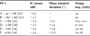
The table contains the mean insertion loss of all states and the phase standard deviation of the measured phase over the specified frequency band. The ideal phase standard deviation for a 4-bit phase shifter is 6.5° (13° for 3-bit and 26° for 2-bit, respectively).
VII. ELECTRONICALLY STEERABLE ANTENNAS
The phase shifters described in the previous paragraph were implemented into complete electronically steerable antennas to prove the concept of phased array antennas using RF MEMS phase shifters. Figure 13 illustrates three electronically steerable antennas, which were designed for different frequencies of operation and used different substrate materials. These antennas are one of very few RF MEMS-based electronically steerable antennas published to date.

Fig. 13. Realized RF MEMS-based electronically steerable antennas. Black arrows indicate the position of the RF MEMS phase shifters.
The first example on the left is an X-band phased array antenna, operating at 9.5 GHz, in which four of the 3-bit switched line phase shifters (D) described earlier in this paper, are integrated [Reference Gautier28]. The antenna itself is realized on an organic RF-substrate with a FR-4 layer underneath for DC-routing. The antenna in the middle is a phased array antenna designed for operation in Ka-band with 3-bit RF MEMS phase shifters (E) implemented [Reference Gautier, Ziegler, Stehle, Schoenlinner, Prechtel and Menzel30]. The complete antenna structure is based on LTCC material, which has cavities on the backside for the integration of the four RF MEMS chips. The RF-distribution network is realized in stripline configuration inside the LTCC multi-layer and the antenna elements are fabricated on the front side of the antenna. Finally, the antenna on the right side is designed to operate in W-band and contains 28 packaged RF MEMS phase shifters (F). The antenna is fabricated on an organic RF-substrate, while the RF-distribution network is realized on LTCC material.
The first two antennas (X-band and Ka-band) were already measured and the performance of the X-band antenna is illustrated in Fig. 14 as an example. It shows the measured H-plane radiation characteristic of the antenna for three switching states of the phase shifters (−15, 0, and +15°). The depicted patterns assume well-formed scanned main beams in the −17, −2, and +12° directions of the H-plane. The side lobe level is −8.8, −9.2, and −6.7 dB for the −17, −2, and +12° oriented main beams, respectively. These relatively high side lobe levels can be explained by the quantization error due to the digital nature of the phase shifters and an inaccuracy in the integration of the phase shifters.

Fig. 14. Measured performance of the X-band electronically steerable antenna.
VIII. SUMMARY AND OUTLOOK
The EADS RF MEMS switch concept was developed since 2003 with a strong focus on reliability and simplicity, while achieving outstanding RF performance. This concept was verified experimentally, showing a high number of switching cycles without visible degradation, robustness with respect to temperature, a switching speed below 10 µs, and record high RF-power handling capability in hot switching mode of more than 9.8 W at 14 GHz. The technology was applied to a number of circuits, demonstrating its RF performance as well as its design flexibility in terms of insertion loss, isolation, frequency range of operation, and bandwidth. As examples, SPSTs, SPMTs, tunable filters, phase shifters, and electronically steerable antennas between 6 and 100 GHz were presented in this document.
ACKNOWLEDGEMENT
The technological development in this work was partly supported by the German Bundesministerium für Bildung and Forschung (BMBF) under the contract “RadarAuge” (#16SV2078) and by the European Commission within the 6th framework program in the frame of the projects 3DµTune (IST-2005-027768) and RETINA (AST4-CT-2005-516121).
 Bernhard Schoenlinner was born in Trostberg, Germany, in 1973. He received his Dipl.-Ing. degree in electrical engineering in 2000 from the Technische Universitaet Muenchen, Munich, Germany and he received his Ph.D. degree in electrical engineering in 2004 from The University of Michigan at Ann Arbor, USA. Since 2004, he is with EADS Innovation Works in Ottobrunn, Germany, as a research engineer in the Microwave Technologies Team. His work focuses on advanced microwave and millimeter wave circuits and subsystems for aeronautic and space applications and he is responsible for managing national and international research projects.
 Armin Stehle was born in Biberach/Riß, Germany, in 1980. He received his Dipl.-Ing. degree in electrical engineering in 2005 from the University of Ulm, Germany and his Dr.-Ing. degree in electrical engineering in 2010 from Saarland University, Germany. From 2005 to 2009 he was with EADS Innovation Works, in Ottobrunn, Germany, where his research interests were on RF-MEMS. Since 2009, he is with EADS Cassidian Electronics in Ulm, Germany, as a research engineer. The focus of his work are T/R-modules and MMICs for radar applications in space.
 Christian Siegel studied electrical engineering at technical university Munich. He has done his Ph.D. on the development of a RF-MEMS switch at the innovation works of EADS in Ottobrunn. Now he is working in the product development on MEMS microphones at EPCOS AG in Munich.
 William Gautier received his master's degree from the “Ecole Nationale d'Ingenieurs de Brest”, France, in 2005. Between 2006 and 2008, he worked toward his Ph.D. in the Microwave Team of EADS Innovation Works in Ottobrunn, Germany. He received his Ph.D. from the University of Ulm, Germany, in 2011. Since January 2009, he is with the Antenna Competence Centre of EADS Cassidian Electronics in Ulm, Germany.
 Benedikt Schulte received the diploma degree in electrical engineering from the University of Siegen, Siegen, Germany, in 2008. He is currently working toward the Ph.D. degree in electrical engineering at EADS Innovation Works, Ottobrunn, Germany. His research interests include highly integrated microwave front-ends (e.g. tunable filters and electronic steerable antenna arrays) for communication and radar systems.
 Sascha Figur received his Dipl.-Ing. (FH) degree in electrical engineering (2007) and his M.Sc. degree in information technology (2009) from Fachhochschule Münster Abteilung Steinfurt, Germany. Currently, he is working on his Dr.-Ing. at EADS Innovation Works, Ottobrunn, Germany, where his research interests are on RF-MEMS-based matching and switching networks.
 Ulrich Prechtel received his diploma in physics from the Technische Universitaet Muenchen, Munich, Germany in 1985. Subsequently, he joined the MBB Central Research Lab in Ottobrunn, where he developed manufacturing technologies for high-energy radiation detectors and IR-focal plane arrays. From 1995 he successfully worked on the research and industrialization of several different types of silicon-based MEMS-type micro-sensors for automotive and aerospace applications. Since 2002, he is responsible for the microwave technology team of EADS Innovation Works, in Ottobrunn, Germany, in which he is focusing on the investigation and exploitation of new RF-devices and subsystems for emerging aerospace and security applications.
 Volker Ziegler received his Dipl.-Ing. degree in electrical engineering and his Dr.-Ing. degree (with honors) both from the University of Ulm, Germany, in 1997 and 2001, respectively. From 2002 until 2003, he was a member of the “Knowledge Exchange Group for Research and Technology” at the DaimlerChrysler AG in Stuttgart, Germany. Since January 2003, he is working with EADS Innovation Works, in Ottobrunn, Germany. He is an EADS Expert for “Microwave Technologies and Systems” and is responsible for the acquisition and managing of national and international research projects in the field of key microwave technologies for advanced radar and communication systems.


