


I. INTRODUCTION
Monolithic integration of the radio frequency microelectromechanical systems (RF-MEMS) switches has advantages over the hybrid integration techniques such as bond-wire or flip-chip due to their less parasitics. The integration of the RF-MEMS switches into a 0.25 µm SiGe BiCMOS technology has been demonstrated in [Reference Kaynak1] and showed valuable results for this integration technique with respect to reliability, repeatability, and the yield issues [Reference Kaynak2]. The integration of the RF-MEMS switch into 0.13 µm SiGe BiCMOS process technology gives the possibility to use RF-MEMS components together with very high-performance heterojunction bipolar transistors (HBTs) [Reference Rücker, Heinemann and Fox3] and provides circuits with unprecedented low attenuation, to be used in antenna switching matrices and phase shifters [Reference Chaloun4].
The developments of RF-MEMS switches in literature are mostly below 40 GHz as a result of the interest in RF-MEMS devices for the commercial applications. With the high-performance semiconductor technologies of today, radar and imaging applications are moving toward the upper part of the mm-wave spectrum and even beyond. A promising application of the RF-MEMS switches at 140 GHz is their use in radar front-ends for active imaging systems (http://project-nanotec.com/). In [Reference Valenta5], a transceiver IC with novel fully integrated differential RF-MEMS SPDT switch for short-range F-band radar systems is presented. Lately, an RF-MEMS-based single-pole double-throw (SPDT) switch is presented in D-band with the lower insertion loss and the higher isolation values compared with the field-effect transistor and HBT-based SPDTs [Reference Tolunay Wipf6].
RF-MEMS switches in BiCMOS processes [Reference Du7] have proven that they can be solutions for applications, which require low insertion loss and high isolation even up to 250 GHz [Reference Du8]. Although the RF-MEMS switches have good RF performances in all the mm-wave range, packaging is still the challenge on the way to their commercialization. A good RF-MEMS package should not only provide the interface to the next level, but should also be cost and area effective. Furthermore, it should be preferably fabricated using wafer-level processes to increase the throughput thus decrease the cost. In wafer bonding approaches of wafer-level packaging (WLP), the cost of at least one lid wafer is added to the total production cost [Reference Morris and Cunningham9]. These additional lid wafers can also add more process steps such as wafer grinding or chemical mechanical polishing. The wafer bonding approach not only increases the cost, but also requires additional area around the MEMS devices to accommodate the cap. Indeed, WLE [Reference Candler10–Reference Barriere12] has advantages over the WLP with wafer bonding approach in terms of cost and area. Predictably, WLE approach is also the chosen method for the well-known commercial packaged MEMS devices [Reference Gaddi13, Reference Morris, Natarajan, Qizheng and Steel14].
In the direction of their commercialization, development of an accurate EM model is essential in order to optimize the RF performances of the WLE RF-MEMS switches. With a three-dimensional (3D) finite-element-method (FEM) solver, it is possible to estimate the RF performances of a WLE RF-MEMS switch. However, an accurate EM model needs a careful modeling approach since one of the key elements, the contact air capacitances in both on and off-states of the switch are not known before its fabrication. The contact air capacitances can vary due to process variations. In order to model the on and off-state of the RF-MEMS switch accurately the contact capacitances of the fabricated RF-MEMS switch should be measured. With the known contact area of the switch and the measured contact air capacitances, the distance between the RF-signal line and the released membrane can be calculated by the simple parallel plate capacitance formula. Afterwards the calculated distance can be given into the EM model for the accurate EM simulations.
Beside an accurate EM model a pure small-signal model of the WLE RF-MEMS switch is also necessary especially for the circuit designers to predict the RF-behavior of the designed circuits using the switch. A small-signal model of the WLE RF-MEMS switch increases the simulation speed remarkably compared with an EM model and gives the possibility to simulate the switch with various circuits in a system level. For mainly these reasons, we have developed a lumped model of the WLE RF-MEMS switch in Keysight ADS [15] and integrated this model into the design kit of a 0.13 µm SiGe BiCMOS process technology.
This paper is the extended version of the conference paper in [Reference Tolunay Wipf16] and contains the technology, fabrication, electromagnetic (EM) modeling, measurements, and the small-signal modeling of the thin-film wafer-level encapsulated RF-MEMS switch. To the best of authors’ knowledge, the demonstrated results provide the first wafer-level encapsulated (WLE) RF-MEMS switch, which operates with state-of-the-art RF performances in D-band in literature. With the developed encapsulation process, the WLE RF-MEMS switch is packaged in one clean room during the BEOL fabrication process. The fabricated WLE RF-MEMS switch provides beyond state-of-the-art insertion loss of better than 0.67 dB in all D-band.
II. WLE RF-MEMS SWITCH IN 0.13 μM BICMOS TECHNOLOGY
In IHPs 0.25 µm SiGe BiCMOS technology, the RF-MEMS switch is realized by using Metal1 as the high-voltage (HV) electrodes, Metal2 (M2) as the RF-signal line and Metal3 (M3) as the suspended movable membrane [Reference Kaynak1]. In comparison with the five metallization layers of the IHPs 0.25 µm BEOL, the 0.13 µm BEOL consists of seven metallization layers with different metal thicknesses and distances between them. With IHPs 0.13 µm SiGe BiCMOS technology, the capacitive RF-MEMS switch is developed between Metal4 (M4) and TopMetal2 (TM2). In order to minimize the substrate couplings, the RF-signal line is shifted up to Metal5 (M5) instead of the M2. Moreover, the movable membrane is thicker in 0.13 µm technology and it significantly changes the electro-mechanical behavior, the RF performance and the fabrication process. In summary, the RF-MEMS switch in 0.13 µm BiCMOS technology is realized with M4 HV electrodes, M5 RF-signal line, TopMetal1 (TM1) movable membrane, and a TM2 plate with releasing holes is placed on top of the RF-MEMS switches for the wafer-level encapsulation.
Figure 1 shows the schematic cross-section of the WLE RF-MEMS switch in IHPs 0.13 µm SiGe BiCMOS technology. Integration of the RF-MEMS switch starts with the standard BEOL flow of the passives. Before the releasing process, TM2 of the RF and DC pads and the TM2 grid of the RF-MEMS switches are reached with the passivation opening. With the defined etching area, the RF-MEMS switches are released by hydrofluoric acid vapor phase etching (HFVPE) through the TM2 grid down to M4 HV electrodes (Fig. 2). The last steps of the process flow include the 4 µm-thick high deposition rate (HDR) oxide deposition on the TM2 grid to close the open holes and have the RF-MEMS switches encapsulated. Finally, the HDR oxide covered pads are reopened by reactive ion etch (RIE) to provide electrical connections for the measurements (Fig. 3).

Fig. 1. The schematic cross-section of the 0.13 µm BiCMOS process technology, including the embedded WLE RF-MEMS switch.

Fig. 2. The scanning electron microscopy (SEM) image of the released RF-MEMS switch before the wafer-level encapsulation (including the focus ion beam (FIB) cross-section).

Fig. 3. The SEM image of the WLE RF-MEMS switch (including the FIB cross-section).
For the success of the wafer-level encapsulation, different design modifications are done and process parameters are optimized. In detail, the TM2 grid's hole size was one of the most important design parameter for both the HFVPE and the wafer-level encapsulation. For the investigation of the hole size impact, the quadratic hole sizes are varied with the side length of 1.25, 1.5, 1.75, and 2.0 µm. Together with the TM2 thickness of d = 3 µm it results in aspect ratios (AR = d/a) from 2.4 down to 1.5. Besides during the varied hole sizes, the distances between the holes are taken identical with the holes sizes.
Beside the hole size, the plasma-enhanced chemical vapor deposition process for the HDR oxide deposition is optimized to achieve the required low step coverage. By minimizing the process temperature of the HDR oxide deposition it is also intended to reduce its influence on the active elements of the front-end-of-line and on the mechanical behavior of the RF-MEMS switch. Consequently, a maximum temperature of 200°C for HDR oxide deposition has been developed to achieve closing of the TM2 grid holes.
As a result of the variable TM2 grid hole size investigation, successfully encapsulated RF-MEMS switches are achieved with an AR of 2.4 and 2.0 (Figs 4(a) and 4(b)). With an AR of 1.7, a carbon containing material inside the closing holes is determined by energy-dispersive X-ray spectroscopy (EDX), which is coming from the spin-coating of the photoresist mask before the RIE opening of the pads (Fig. 4(c)). The photoresist enters from the TM2 grid holes in case of a not fully closed TM2 grid holes. Clearly with an AR of 1.5, a fully closed encapsulation also could not be achieved (Fig. 4(d)). Indeed, with AR of 2.4 and 2.0 it was possible to close the TM2 grid holes while pretending the unwanted HDR oxide deposition through the holes into the cavity.

Fig. 4. The focused ion beam SEM images of the wafer-level encapsulation on the aspect ratios (a) AR = 2.4, (b) AR = 2.0, (c) AR = 1.7 (including the EDX analysis), and (d) AR = 1.5.
III. EM MODELING
During the development of the RF-MEMS switch in the 0.13 µm SiGe BiCMOS technology, an accurate EM model is built up in ANSYS HFSS 3D FEM solver (Fig. 5(a)). For the accurate EM model in the 3D FEM solver, the distances between TM1 membrane and M5 RF-signal line for both off (d off ) and on-states (d on ) of the switch are needed to be inserted into the simulator.

Fig. 5. EM simulation model in ANSYS HFSS for D-band BiCMOS embedded WLE RF-MEMS switch (a) with the schematic diagram for the parametric EM simulations for different, (b) d off , and (c) d on values.
The mean value of the distance between the TM1 membrane and M5 RF-signal line in off-state is 900 nm in IHPs 0.13 µm SiGe BiCMOS technology. However, the off and on-state contact air capacitances of the fabricated RF-MEMS switch can vary over the wafer due to process variations such as different surface roughness, metal and oxide thicknesses or stress behaviors of the TM1 membrane. In order to estimate the possible RF performance differences due to the process variations, parametric EM simulations with different d off and d on are performed (Fig. 5(b) and 5(c)). For the insertion loss in the parametric EM simulation the membrane position is swept from 100 nm above the specified TM1 layer until 100 nm below with a step size of 50 nm. Figure 6 shows the change of the insertion loss curves with different d off values. Varying d off by 200 nm leaded to 0.16 dB change of insertion loss at 170 GHz. Furthermore, the parametric EM simulations are extended with different d on values for the isolation curves. The distance d on is stepwise (10 nm) decreased starting from 100 down to 40 nm and the simulation results are shown in Fig. 6. Decreasing d on by 60 nm caused a resonance frequency shift from the upper end of the D-band to the lower end. Briefly, the varying d off due to process variations did not affect the insertion loss tremendously but the resonance frequency shifted significantly with the varying d on (Fig. 6). For this reason we extract the contact air capacitances from the C–V measurements of the RF-MEMS switch to have an accurate 3D FEM result of the D-band RF-MEMS switch especially for the on-state. Based on the extracted contact air capacitances (C off and C on ) and the known contact area of the switch, d off and d on can be calculated using the simple parallel plate capacitor equation and inserted into the EM model.

Fig. 6. The simulated S-parameters of the WLE RF-MEMS switch with varying TM1 membrane and M5 RF-signal line distances due to process variation.
IV. MEASUREMENTS
A) C–V Measurements
The thin-film WLE RF-MEMS switch is initially characterized by C–V measurements. For the C–V measurements, the high-frequency impedance analyzer Agilent E4991 for the range from 1 MHz to 3 GHz is used and the capacitance values are taken from 3 GHz. An Open/Short/Load calibration on an impedance standard substrate (ISS) from Cascade Microtech is applied before measurement of the WLE RF-MEMS switch to remove measurement setup parasitics. The capacitance values are measured for the actuation voltages between −80 to +80 V with 5 V steps. Figure 7 shows the measured C–V graph of the WLE RF-MEMS switch and the extracted contact air capacitance versus actuation voltage graph. Extraction of the contact air capacitances is done with the help of an additional test structure that consists of a RF-signal line without membrane and encapsulation grid. With the test structure, the coupling capacitance (52 fF) from the signal line to the silicon substrate is measured and the contact air capacitances are extracted by its subtraction. The contact air capacitances are extracted as 13.4 fF C off and 149 fF C on with a C on /C off ratio of 11.1. Moreover, it is observed that the pull-in occurs after 50 V and the on-state capacitance is stable after 65 V of actuation.

Fig. 7. The measured C–V graph of the WLE RF-MEMS switch (red) and the extracted contact air capacitance versus voltage graph (black).
B) Scattering parameter measurements
The two port S-parameters of the WLE RF-MEMS switch are measured on wafer from 110 to 170 GHz. For the measurement, a setup from Rhode & Schwarz, consisting of a four-port ZVA24 as VNA/system controller and two ZVA170 Millimeter-Wave Converters, are used. The Cascade 75 µm pitch infinity(R) GSG waveguide probes are connected via a WR6 waveguide s-bend with the millimeter-wave modules. For calibration, the ISS 138–356 is placed together with an RF absorber on an auxiliary ceramic chuck and a full two-port LRRM calibration is performed. To actuate the membrane of the RF-MEMS switch a 100 V Agilent Source Measurement Module E5281B is used.
To the best of authors’ knowledge, the 0.13 µm BiCMOS embedded thin-film WLE RF-MEMS switch is the first RF-MEMS switch in literature, which operates with state-of-the-art RF performances in D-band. The comparison of the measured and simulated S-parameter results of the WLE RF-MEMS switch is given in Fig. 8. The switch shows maximum isolation of 51.6 dB at 142.8 GHz with the insertion loss of 0.65 dB. For the insertion loss curves, the signal reflection due to mismatch is considered by IL = 10 × log (|S 21|2/(1–|S 11|2)). Based on the measured C on and C off capacitances (Fig. 7) and the considered ~1200 µm2 contact area, d off is calculated as 800 nm and d on as 70 nm. The calculated d off and d on values are then inserted into the EM model for the comparison with the S-parameter measurements. The 3D FEM simulation results are in very good agreement with the measured S-parameters in the 110–170 GHz frequency band.

Fig. 8. The comparison of the measured and simulated S-parameters for up-state S 21 (black), insertion loss (blue), and isolation (red) of the WLE RF-MEMS switch.
V. LUMPED-ELEMENT MODELING
Although the 3D FEM solvers provide accurate EM simulation results with the calculated d off and d on values from the extracted contact air capacitances (C off and C on ), lumped-element models give faster simulation results. Furthermore, a lumped model of a RF-MEMS switch [Reference Chawla and Khanna17] increases the usage of the device since with the help of the lumped-model, RF-MEMS switches can be simulated in various circuits on system level. In this study, the lumped-element model of the WLE RF-MEMS switch based on RLC components is developed and simulated in Keysight ADS. The main capacitances for the lumped-element model of the WLE RF-MEMS switch are shown on the process cross-section in Fig. 9.

Fig. 9. The process cross-section of the WLE RF-MEMS switch, including the main capacitances of the lumped-element model.
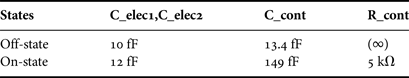
Similar to the EM model, the extracted contact parameters of the switch is necessary for the lumped-element model of the RF-MEMS switch especially in on-state. Figure 10 shows the lumped-element model of the WLE RF-MEMS switch. The extracted contact air capacitances (C_cont), C off of 13.4 fF and C on of 149 fF are used to model the contact region. Furthermore in the on-state model, the contact resistance of 5 kΩ is also considered.

Fig. 10. The lumped-element model of the WLE RF-MEMS switch.
For the S-parameter simulation with the lumped-element model, port1 and port2 are terminated with 50 ohm. The M5 RF-signal line is modeled using RLC components between the two ports and the arms of the membrane are modeled as inductors (L_arm1, L_arm2) with series resistors (R_arm1, R_arm2). C_elect1 and C_elect2 are the parasitic capacitances between the TM1 membrane and the M4 high-voltage electrodes. The values of the RLC elements of the lumped model for both states of the switch are given in Table 1 below. Due to the down bending of the TM1 membrane in on-state, C_elec1 and C_elec2 values are modeled slightly larger compared to the off-state values. Table 2 shows the varied C_elec1, C_elec2 and C_cont values with respect to the states of the WLE RF-MEMS switch.
Table 1. Small-signal component values of the WLE RF-MEMS switch.

Table 2. Small-signal component values of the WLE RF-MEMS switch, varied due to states.
Both the 3D FEM model and the lumped-element model consider the effect of the wafer-level encapsulation on the RF-MEMS switch. For the wafer-level encapsulation to include in the lumped-element model, TM2 plate is modeled with series inductances (L_encap1, L_encap2, L_encap3, L_encap4, L_encap5) and resistances (R_encap1, R_encap2, R_encap3, R_encap4, R_encap5). Additionally for its effect on the RF-MEMS switch, the coupling capacitances (C_encapSL1, C_encapSL2, C_encapSL3, C_encapSL4) between the TM2 plate and the M5 RF-signal line is also inserted into the lumped-model. As a final point, the substrate effects are considered in the model and inserted as parallel capacitance (C_subst) and resistance (R_subst) between ground and the RF-signal lines.
Figure 11 shows the comparison between the measured S-parameters of the fabricated WLE RF-MEMS switch with simulation results of the EM model and the lumped-element model. Both EM model and lumped-element model simulation results are in very good agreement with the measured S-parameter results in the D-band.

Fig. 11. The comparison of the measured, EM modeled and small-signal modeled S-parameters for (a) up-state S 21, (b) up-state S 11, (c) up-state insertion loss, and (d) down-state isolation of the WLE RF-MEMS switch.
Finally, the presented lumped-element model of the WLE RF-MEMS switch is integrated into the IHPs SG13G2 and SG13S process design kits in Keysight ADS. Figure 12 shows the parameterized RF-MEMS cell in the ADS schematic environment including the selectable state parameter between off (up) and on (down)-states. With the integration of the WLE RF-MEMS switch into the design kit, the presented WLE RF-MEMS switch can be combined in system-level simulations with the IC components.

Fig. 12. Design kit integrated WLE RF-MEMS switch in Keysight ADS.
VI. CONCLUSION
This paper has presented the EM modeling and lumped-element modeling of a thin-film WLE RF-MEMS switch embedded in IHPs 0.13 µm SiGe BiCMOS process technology for D-band applications. Both developed models show a very good agreement with the measured S-parameter results. With the developed WLE RF-MEMS switch, maximum isolation of 51.6 dB at 142.8 GHz is achieved with a 0.65 dB insertion loss.
ACKNOWLEDGEMENTS
The authors thank to the team of the IHP pilot line for excellent support. This work was supported by the European Commission under the Contract no. 288531-NANOTEC (www.project-nanotec.com).
 Selin Tolunay Wipf was born in May 1987. She received her B.S. degree from the Electronics Engineering program of Sabanci University, Istanbul, Turkey, in 2010 and her M.S. degree from the Electrical and Electronics Engineering Department of Bogazici University (BUEE), Istanbul, Turkey, in 2012. She joined the MEMS group of IHP Microelectronics in 2012 and has been working on the RF optimizations of the MEMS devices for the mm-wave applications. Since 2015, she is a member of the Heterointegration group of IHP with a focus on the RF design, optimization, and characterization of the RF-MEMS switches above 100 GHz applications. Mrs. Selin Tolunay Wipf was involved in the FP7 projects UTMOST in Bogazici University, FLEXWIN, and NANOTEC in IHP microelectronics.
 Alexander Göritz was born in 1981. He studied Electrical Engineering (microelectronics – semiconductor technology) at the Technische Universität Dresden. He received the Dipl.-Ing. degree in 2011. In 2012, he joined IHP Technology Department and started working on the development of MEMS for mm-wave applications and their thin-film wafer-level encapsulation. In parallel, he applies and improves the HF vapor phase-etching process to release the established MEMS devices. Since 2014 he has been involved in the creation and application of general Back-End-Of-Line (BEOL) process flows to realize BEOL wafer for cost-efficient test platforms for passive devices. Meanwhile he also participates in the development of microfluidic channel, bolometer, and graphene-based devices. Mr. Alexander Göritz worked on the FP7 projects, FLEXWIN, and NANOTEC.
 Matthias Wietstruck was born in 1984. He graduated with a diploma in microsystems technology from the University of Applied Sciences in Berlin in 2009. He joined the IHP Technology Department in 2010 and has been working in the area of MEMS for mm-wave applications. Since 2013 he has been started the research activities in the area of through-silicon via technology and heterogeneous 3D integration at IHP. His current research focuses on the design and integration of TSVs into the BiCMOS technology as well as temporary and permanent wafer bonding for heterogeneous 3D integration. Since 2015, he is heading the Heterointegration group at IHP.
 Christian Wipf joined the Technology Department of IHP in 2005 and received his M.Sc. in Electrical Engineering from the University of Technology, Cottbus, Germany, in 2008. He is working in the field of characterization of electronic devices and circuits up to and above 100 GHz within the Technology Department. Furthermore, he is designing high voltage control circuitries for MEMS matrix applications.
 Bernd Tillack received the Ph.D. degree in 1980. In 1981, he joined the IHP Frankfurt (Oder), Germany, as a staff member of the process technology. Since 2014 he has been heading the IHP as scientific director. His research interests include SiGe BiCMOS technology development following the “More than Moore” strategy for embedded system applications. Since 2008 he has a professorship for Si-based high-frequency technologies at the Berlin Institute of Technology (TU Berlin).
 Andreas Mai received his diploma in physics from the Technical University of Brandenburg (Cottbus) together with “Advanced Micro Devices” (AMD) in 2006. Subsequent he joined the IHP Technology Department. He worked in the Process Integration group on the development of a 130 nm SiGe-BiCMOS technology with for mm-wave applications and focus on the integration of RF-LDMOS transistors. He received his Ph.D. in 2010 and became the project leader for the technical coordination, yield enhancement and technology stabilization of IHPs MPW-technologies. In 2013, he got the position as group leader of the “Process Integration”. Since 2015 he has been the acting technology department head with the main responsibilities for operation of IHPs 200 mm-SiGe-BiCMOS pilot line and technology service activities of IHP. Dr. Mai is the IEEE member and chairs the processing committee of the ECS SiGe, Ge & Related Compounds Symposium.
 Mehmet Kaynak received his B.S. degree from Electronics and Communication Engineering Department of Istanbul Technical University (ITU) in 2004, took the M.S. degree from Microelectronic program of Sabanci University, Istanbul, Turkey in 2006 and received the Ph.D. degree from Technical University of Berlin, Berlin, Germany in 2014. He joined the technology group of IHP Microelectronics, Frankfurt (Oder), Germany in 2008. From 2008 to 2015, he has led the MEMS development at IHP. Since 2015, he has been the department head of technology group at IHP. Dr. Kaynak is being affiliated as Adjunct Professor at Sabanci University, Turkey. Dr. Kaynak has published over 100 peer-reviewed journal and conference publications as an author or co-author. He has granted seven patents.


