


I. INTRODUCTION
The wideband band-stop filters (BSFs) are important in Ultra-wide band communication system, a leading technology that requires at least 500 MHz or relative bandwidth of more than 20% of the center frequency as decided by the federal communication commission and the International Telecommunication Union radio communication sector. The range of frequency is assigned from 3.1 to 10.6 GHz, which is used for a variety of applications, such as medical imaging systems and vehicular radar systems [Reference Jia-Sheng1]. The BSF is one of the most critical design element in microwave systems, as it is used to suppress undesired wideband signals. Numerous types of wide stopband filters have been reported for these systems to confine the spectrum to the assigned frequency band and to solve the problem of interference with a relatively strong narrowband signal [Reference Lei, Sheng and Rui2]. For this purpose, many studies have investigated the design of wideband filters with various configurations [Reference Tu and Chang3–Reference Sarkar, Moyra and Monda17]. However, these filters are relatively large in size and complicated. Without any shunt stub, DGS/DMS, and vias, it is difficult to obtain an attenuation level lower than 20 dB with an fractional bandwidth (FBW) greater than 50% for most of the other filters.
Therefore, in this contribution, a simple microstrip BSF with open stubs and inner T-inverted shape to solve the interference of wideband signals is developed. Additionally, the physical size and performance of the BSF are improved. By using RF4 substrate, this filter has the advantages of low-cost, light weight, ease of fabrication, and implementation.
For this work, a BSF is required to block any signal coming from LTE 1800/1900/2000, GSM 1800(DCS)/1900(PCS), UMTS 1700/1800/1900/2100 bands, more specifically at 1.8 GHz. As time goes on, there are more commercial products or devices operating within this band. More problems occur as more unwanted signals disrupt the operation of other devices within this frequency band. For this reason, the BSF is essential for this consideration, the important parameters are being the center frequency as well as the bandwidth, insertion and the return losses.
The layout of the designed BSFs is shown in Fig. 1 in which the pattern dimensions are analytically extracted by a lossless transmission line model; an electromagnetic simulation is performed using ADS-Momentum and CST-Studio simulators, and the characteristics are validated by simulation for its applications in MW systems.

Fig. 1. (a) Layout of the proposed wideband BSF (A), (b) layout of the proposed wideband BSF (B).
By choosing different open-stubs and open-coupled lines values, various BSFs can be achieved. The bandwidths of the two high selectivity wideband BSFs can be easily adjusted by changing the characteristic impedance and the length of the resonant structures. Two wideband BSF prototypes with 20-dB FBWs of 43.38% (1.42–2.21 GHz) and 50% (1.33–2.21) GHz) are designed and fabricated for demonstration.
II. FILTER DESIGN
The method used in the design shown below consists of using directly connected feed lines on 50 Ω ports. The layout schematic is depicted in Fig. 1 to achieve a center frequency of 1.8 GHz. The microstrip transmission line is bent to get a reduced and compact size.
The proposed circuit structure of the BSF is shown in Fig. 1. The length of the two stubs will be indicated by L = l 1 + l 2. The length of the T-inverted microstrip transmission line will be indicated by L T . Due to the bending loss in the line, the length of the stub is not exactly λ g /2. The calculated values of L and L T are 23.25 and 12.9 mm, respectively. The width, W of the microstrip lines, are not uniform in the entire structure, which is 2.2 mm for l 1, 1.5 mm for l 2, 0.5 mm for L T . The open T-inverted stub, which has a length of 12.9 mm, is used to control the bandwidth and enhance the insertion losses.
Due to the fact that the impedance of the transmission lines in between the two ports has a low characteristic, the T-inverted stub is the key component for building a BSF performance. The input and output feed lines are designed to match the characteristic impedance of 50 Ω for a typical microstrip line.
By combining the structure (a) and (b) of the Fig. 2, two novel compact BSFs (Filter A and Filter B) have been designed. Filters A and B are shown in Fig. 1. Thus, the two stubs resonators are bent 90° to form an L-shaped structure as shown above.

Fig. 2. (a) Structure of the conventional BSF with open stubs, (b) structure of proposed T-inverted shape.
In the first step, the simulation was performed using the Advanced Design System (ADS) simulator Momentum tool. The proposed BST filter is printed on the FR4 substrate with a relative permittivity of 4.4 and a thickness of 1.58 mm, and tangent loss δ = 0.025. The center frequency is 1.8 GHz, and the 10-dB bandwidth is approximately 890 MHz. The detailed dimensions of the layout of the designed BSF are as follows:
The gap g between the two L-stubs is 0.5 mm and it does not have an effect on the filter response. For the input and output ports, two feeds lines are set to a length of 10 mm and width of 3 mm. Figure 1 shows the physical geometry definition of the final layout of these fabricated BSFs. A full-wave simulator CST-MWS and ADS-Momentum has been applied to obtain and efficiently tune the physical dimensions.
A) Equivalent circuit
The equivalent circuit of the microstrip wideband BSF design with open stubs line is depicted in Fig. 3(a), consisting of RLC lumped elements. In this equivalent circuit, the RLC circuit was considered to determine the resonant characteristics; other parasitic capacitances and equivalent resistors are included into the circuit model (the resonance frequency of each inductor depends on its inductance value and parasitic capacitance). Figure 3(a) shows the implemented structure of the BSF in the S-parameters workspace of the ADS software. After implementing this structure, all of its parameters will be selected in order to have an acceptable frequency response. The gap spacing (g) between stubs does not have any effect on the filter response; therefore, it is shown as dashed lines.
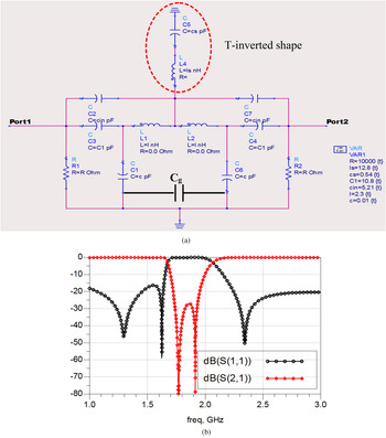
Fig. 3. (a) Equivalent circuit model of the designed wideband BSF. (b) Response of the equivalent model.
B) Optimization process of the BSF design
The optimization process is needed to make sure the design fulfils the requirement of the BSF specification. In this work, the length of the two L-open stubs and the length of inner T-inverted shape are optimized. After the simulated result is obtained, the results are analyzed to choose the best values that satisfy the BSF specifications.
C) The influence of l 2 on the performance of the proposed filter
The length l 2 of L-open stub was increased up to 10 mm, starting with an l 2 = 5 mm (Fig. 4). From the graph bellow, the center frequency is measured between 1.4 and 2.4 GHz for all different values. However, the nearest to 1.8 GHz is the filter design with l 2 = 10 mm. Subsequently, the filter with l 2 = 10 mm has higher return losses and lower insertion losses compared with other values. Therefore, for this first set of optimization, the value of l 2 design is chosen.

Fig. 4. Effect of l 2 on the filter response.
D) The influence of L T on the performance of the proposed filter
The length of the inner T-Inverted stub is increased up to 13.6 mm, starting with an L T = 10 mm (Fig. 5). Similar to the analytical approach in Section A, only the value of L T is changed while the other parameters are determined. The T-inverted shape geometry is the main feature in designing wideband stopband filter. Thus, to make sure the design fulfills the wide stop band specification. The L T length is varied for four different lengths, which are 10, 12, 13, and 13.6 mm. In terms of a center frequency around 1.8 GHz, two pass bands, and FBW more than 40%, the filter design with L T = 13 mm is required. In addition, this design also has the best return loss performance, which is near to 0.3 dB. Therefore, for this set of optimization, the length L T = 13 mm is chosen.

Fig. 5. L T effect on the filter response.
III. MEASUREMENT RESULTS
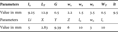
The designing method is based on software-oriented simulations focusing on realizing size compactness, reducing insertion, return and transmission losses. The initial dimensions of the structure can be determined and the final design is obtained by the full-wave simulation. The optimal dimensions of the presented filter are in Table 1.
Table 1. Dimensions of the BSF (Filter A).
The simulated results of the proposed BSF structures are shown in Fig. 6. As it can be seen, three transmission zeros are achieved to widen the bandwidth of the stopband, several transmission poles are also introduced to improve the performance within passbands.

Fig. 6. Comparison results obtained by ADS-Momentum & CST-MW Studio software.
A) Comparison results
In this step, the designed BSF will be analyzed by CST-MW Studio in order to compare the obtained response. The insertion loss S 21 and return loss S 11 are 25-dB and 0.44-dB, respectively, at a center frequency of 1.8 GHz, which are in accordance with the results obtained by Momentum tool as depicted in Fig. 6. In this graphical plot, the simulation results are merged for comparison. The results of the proposed BSF generated using ADS-Momentum, were compared with those generated using CST-MWS.
The passband insertion loss is less than 1.0 dB in the range of 0–1.2 GHz and smaller than 1.0 dB in the range of 2.35–3.0 GHz. The return loss in both cases is superior to 15 dB.
As shown in Fig. 7(a), the maximum measured group delay is 1.2 ns while the minimum is 0.44 ns in the low passband (ranging from 0 to 0.1.35 GHz). As for the upper passband, group delay is shown in Fig. 7(b), the maximum is 1.48 ns, and the minimum is 0.51 ns in the range of 2.33–3.0 GHz.

Fig. 7. (a) Group delay performance of the low passband and (b) the upper passband of the BSF.
B) Current distribution
The wideband BSF was analyzed by CST-MWS to verify the flow of the current density in the BSF pattern. The frequencies from DC to 1.3 GHz and from 2.4 GHz to 3 GHz have a better current distribution. However, at 1.8 GHz, the current distribution is totally stopped, which indicates that the frequency is rejected completely. These current distributions are shown in Fig. 8.

Fig. 8. Simulated current distributions of the optimized wideband BSF at (a) 1.8 GHz, (b) from DC to 1.3 GHz, and (c) from 2.4 to 3 GHz.
In (a), there is a high concentration around port 1, but no current distribution around port 2. This asymmetric current distribution along the structure presents the stop-band behavior. Filter B is designed along the same procedure as depicted in the previous sections.
Figure 9 shows the physical layout of two fabricated BSFs (the left is Filter A and the right is Filter B).

Fig. 9. Photograph of the fabricated microstrip BSFs.
The measured results of Filter A show that a stopband from 1.4 to 2.16 GHz with the return loss less than 0.77 dB and the insertion loss more than 25.5 dB is obtained. A bandwidth of 20-dB is about 42.6%.
The simulated and measured results of Filter B are shown in Fig. 11. From Figure 11, we can see that the return losses of Filter B is less than 0.79 dB, and the insertion losses is more than 30 dB in the center of the stopband.
The simulated results as shown in Figs 10 and 11 are accomplished by a full-wave simulation tool while the measurement is performed by using MS2028C Anritsu VNA (Master Vector Network Analyzer) in microwave laboratory. Nevertheless, the full-wave simulated and measured scattering parameters are in good agreement. Finally, in order to clarify the advantages of this proposed filter, a comparative approach with recent publications are used to determine its performance as showed in Table 2.
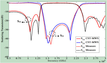
Fig. 10. Simulated and measured results of the filter A (the operating frequency is 1.8 GHz).

Fig. 11. Simulated and measured results of the filter B (the operating frequency is 1.82 GHz).
Table 2. Comparison of the BSF performances.

Table 2 shows the comparison of the proposed filter with other reported wideband BSFs. The proposed filter has the potential of applying to RF/Microwave integrated circuits.
IV. CONCLUSION
A two optimized microstrip wideband BSFs with two open stubs and T-inverted stub are designed for wideband communication system applications, which were successfully developed by using two different softwares, based on an FR4 substrate. The microstrip transmission line was bent to reduce its length at the cost of a bending loss that showed good performance of wideband BSFs. The simulated results indicated that the insertion losses were below 20 dB with a sharp and wide rejection. A good agreement between simulation results has been found, showing the reliable design process. The 20 dB bandwidth is 890 MHz, suitable for the wideband system. Therefore, this design was done to fit in with other practical applications in the targeted communication system.
ACKNOWLEDGEMENT
The authors would like to thank the staff members of the STRS Laboratory of INPT in RABAT for providing the technical assistance in this research, for support with regard to simulation software and facilities.
 Lahcen Yechou was born in Chefchaouen, Morocco, in 1984. He received the license degree in Physics from Abdelmalek Essaadi University, Tetouan, Morocco, in 2010. He received a Master degree in Electronics and Telecommunications from Abdelmalek Essaadi University of Tetouan, Morocco, in 2012. He is currently working toward the Ph.D. degree in embedded systems at Institute National of Posts and Telecommunications (INPT), Rabat Morocco. His research interests include the analysis and design of microwave filters.
 Abdelwahed Tribak was born in Larache, Morocco, in 1981. He received the M.Sc. degree in physics from Abdelmalek Essaadi University, Tetouan, Morocco, in 2006, a Master degree in Communications Engineering from the University of Cantabria, Santander, Spain, in 2008, and also received the Ph.D. of Telecommunication degree in 2011, from the University of Cantabria, Santander, Spain. Since 2006–2011, he has been with the Department of Communications Engineering, University of Cantabria. Since 2011 he is an associate Professor in the National Institute of Post and Telecommunication, Rabat, Morocco. His main area of activities is microwave circuits and systems; antenna feed subsystems for satellite and radio-astronomy applications.
 Kacim Mohamed was born in Beni Mellal, Morocco, in 1952. He received a DUT Electric Genius, automatic option in 1977 in Toulon France, a license (Bachelor's degree) and a control (Master's Degree) EEA from the university Paul Sabatier in Toulouse France in 1979, a POST-GRADUATE DIPLOMA from Automatic in the LAAS in Toulouse France in 1980, a Doctorate 3rd cycle, Automatic Option in the LAAS in Toulouse France in 1982, and also received a Doctorate of State Es-Sciences Appliqués of the university Mohamed V, Engineers’ Mohammadia Rabat school-Morocco in 1996, In 1982, he was recruited at time (weather) as Professor to the National Institute of the Posts and the Telecommunications of Rabat-Morocco, His domain as head teacher (main clause) of activity, is the Analysis, the Synthesis, and the Command of the systems.
 Jamal Zbitou was born in Fes, Morocco, in June 1976. He received the Ph.D. degree in electronics from Polytech of Nantes, the University of Nantes, Nantes, France, in 2005. He is currently an associate Professor of Electronics in FPK University Hassan 1st, Settat, Morocco. He is involved in the design of hybrid, monolithic active, and passive microwave electronic circuits.
 Abdelmalik Bouyahyaoui was born in Assilah, Morocco, in 1955. He received a control (master's degree) EEA (Electronic, Electrotechnic Automatic) from the university Paul Sabatier in Toulouse France in 1980 and a Doctorate 3rd cycle, Microelectronics option in the LAAS in Toulouse France. He was recruited at time as Professor to the National Institute of the Posts and the Telecommunications of Rabat-Morocco, His main area of activities is the very high frequency oscillators, commanded oscillators in very high frequencies, and the phase locked loop.
 Angel Mediavilla Sanchez was born in Santander, Spain, in 1955. He graduated in 1978 and received the Doctor of Physics (Electronic) degree with honors in 1983, both from the University of Cantabria, Santander, Spain. From 1980 to 1983 he was Ingenieur Stagiere at THOMSON-CSF, France. He is currently head of the Communications Engineering Department at the University of Cantabria. He has a wide experience in the analysis and optimization of nonlinear microwave active devices. His research interests are nonlinear MESFET/HEMT and HBT device modeling with special application to the large signal computer design, and new waveguide structures for antenna feed systems.


