


I. INTRODUCTION
Multi-band bandpass filters (BPFs) have became a key component of radio-frequency front-end in multi-band/multi-service wireless communication systems. In past, the multi-band BPFs were realized with several single-band filters [Reference Miyake1] or using the external feed lines [Reference Kuo and Cheng2]. However, such approach requires large circuit size, high passband losses, and external combining networks. Stepped impedance resonators (SIRs) are known and usually used to shift the high-order resonant modes for developing the multi-band BPFs. Recently, triple-passband BPFs have been implemented by using the SIRs [Reference Chen and Chu3, Reference Chen, Huang and Wu4]. However, the dimensions of these works are still large because the SIRs are arranged by the direct-coupling or cross-coupling structure on the single substrate. Recently, stub-loaded resonators (SLRs) are the newly structure for developing the triple-passband filters [Reference Zhang, Xue and Hu5, Reference Chen, Weng and Chang6]. In [Reference Zhang, Xue and Hu5], the tri-band filter employs two sets of SLRs and half-wavelength resonators for achieving compact size and high passband selectivity. However, the uniform impedance resonators (UIRs) are used that the design freedom is limited when choosing the every passband frequencies. In [Reference Chen, Weng and Chang6], the tri-band filter using the stub-loaded SIRs was proposed for the first time. However, circuit size and wide stopband are an issue and needed to further improve. To miniaturize the circuit size, the multi-band filter using embedded open-loop ring resonators was proposed in [Reference Hsu, Chen and Chuang7]. The filter without using the external impedance transformer can further miniaturize the circuit size. The idea is good; however, the via-hole of shorted circuit would cause a complex integration in packaging. In this paper, we propose a new multi-layered triple-passband filter using the embedded SIRs on the top layer and stub-loaded SIR on the bottom layer for the first time. The embedded SIRs are designed to have two resonant paths (path 1 for 1.8 GHz and path 2 for 2.4 GHz) and its resonant modes (1st and 2nd modes) can be easily determined to very close or far away for highly design freedom. Each resonant path generates its own passband and there is good isolation between the three passbands. The stub-loaded SIR is connected with the open-circuited stub-loaded branches to control the transmission zeros individually at 3rd passband edges. The measured results are in good agreement with the full-wave electromagnetic simulation [8] results.
II. FILTER DESIGN
Figure 1 shows the coupling structure and three-dimensional (3D) view of the proposed filter. In Fig. 1(a), resonators 1 and 3 indicate the embedded SIRs with two coupling paths for achieving dual-passband (resonators 1 I and 3 I for 1.8 GHz and resonators 1 II and 3 II for 2.4 GHz). The resonator 2 III indicates the cross-shaped stub-loaded SIR (for 3.5 GHz) and cross-coupled to resonators 1 and 3. The green dashed lines (path 3) show the coupling path to the source and load. The multi-layered filter consists of the coupled embedded SIRs on the top layer and the cross-shaped stub-loaded SIR on the bottom layer, as shown in Fig. 1(b). The embedded SIR is designed to generate 1st passband at 1.8 GHz and 2nd passband at 2.4 GHz. The stub-loaded SIR is designed to generate 3rd passband at 3.5 GHz. The features of the triple-passband filter are the use of multi-layer technique to further reduce the circuit size and providing the very close triple-passband with high in-band isolation and good passband selectivity. The three resonators were used to generate a triple-passband response and having the wide stopband below −15 dB isolation from 4 to 8 GHz. In this study, the even- and odd-modes of the embedded SIR can be controlled individually, resulting in the dual-band filter with very close passbands. Therefore, each passband can be implemented individually and each coupling coefficient between adjacent resonators can be extracted separately at the three specific passbands. The multi-layered filter could not only save the circuit size, but also generate the cross-coupling effects, which the extra transmission zeros near the passband edges can be easily achieved [Reference Wu, Chen and Chen9].

Fig. 1. (a) Coupling structure and (b) 3D view of the proposed filter (h 1 = h 2 = 0.787 mm, Resonators 1 and 3: embedded SIR, Resonator 2: stub-loaded SIR, Path 1 for 1.8 GHz, Path 2 for 2.4 GHz, and Path 3 for 3.5 GHz).
A) Resonant modes of the embedded and stub-loaded SIRs
Figure 2 shows the equivalent transmission line model of the embedded and stub-loaded SIRs. The embedded SIR is composed of a conventional half-wavelength SIR (2[(Z 1, θ 1), (Z 2, θ 2)] for path 1 at 1.8 GHz) and an embedded SIR ([(Z 1, θ 1), (Z 2, θ 2), (Z 3, θ 3) (Z 4, θ 4)] for path 2 at 2.4 GHz), as shown in Fig. 2(a). The common section of [(Z 3, θ 3) and (Z 4, θ 4)] for path 2 can effectively control the resonant mode very close to the 1st passband (1.8 GHz for path 1) and resulting the highly in-band isolation. By properly tuning the dimension of the embedded SIR, such as impedance ratio (K 1 = Z 2/Z 1 and K 2 = Z 5/Z 6) and length ratio (α 1 = θ 2/(θ 1 + θ 2) and α 2 = θ 5/(θ 5 + θ 6)), the arrangements of every resonant modes become more flexible. The stub-loaded SIR is formed by the cross-shaped configuration, which is composed of the horizontal- and the vertical-resonators, as shown in Fig. 2(b). The horizontal SIR with [(Z 5, θ 5), (Z 6, θ 6)] is designed to generate the 3rd passband at 3.5 GHz, and the vertical open-circuited SLRs with (Z 7, θ 7) and [(Z 8, θ 8), (Z 9, θ 9)] are designed to provide the transmission zeros near the passband edges. The embedded SIR can be analyzed to even- and odd-modes along the symmetric plane. The resonant modes of the resonator can be derived by setting Y ine = Y ino = 0 and expressed as
 $$Y_{ine} = - j\displaystyle{\matrix{Z_2 \left(\cot \!\theta_1 - K_1 \tan \!\theta_2 \right)\cr + \,\left(Z_S \cot \!\theta_S \right)\left(K_1 + \cot \!\theta_1 \tan \!\theta_2 \right)} \over Z_ 2 Z_S \cot \!\theta_S \left(\cot \!\theta_1 - K_ 1 \tan \!\theta_2 \right)} = 0\comma$$
 $$Y_{ino} = \displaystyle{1 \over jZ_2} \displaystyle{K_1 - \tan \!\theta_1 \tan \!\theta_2 \over \tan \!\theta_1 + K_1 \tan \!\theta_2} = 0\comma$$
where
 $$Z_S = - jZ_3 \displaystyle{Z_4 \cot \!\theta_4 - Z_3 \tan \!\theta_3 \over Z_3 + Z_4 \cot \!\theta_4 \tan \!\theta_3} \quad {\rm and} \quad \theta_S = \theta_3 + \theta_4.$$
The input impedance Z T of the stub-loaded SIR
 $$Z_T =\displaystyle{Z_A Z_B \over Z_A +Z_B} = \displaystyle{Z_8 Z_7 \cot \!\theta_7 \left(Z_9 \cot \!\theta_9 - Z_8 \tan \!\theta_8 \right)\over \matrix{jZ_7 \cot \!\theta_7 \left(Z_8 + Z_9 \cot \!\theta_9 + \tan \!\theta_8 \right)\cr + \,jZ_8 \left(Z_9 \cot \!\theta_9 - Z_8 \tan \!\theta_8 \right)}}.$$
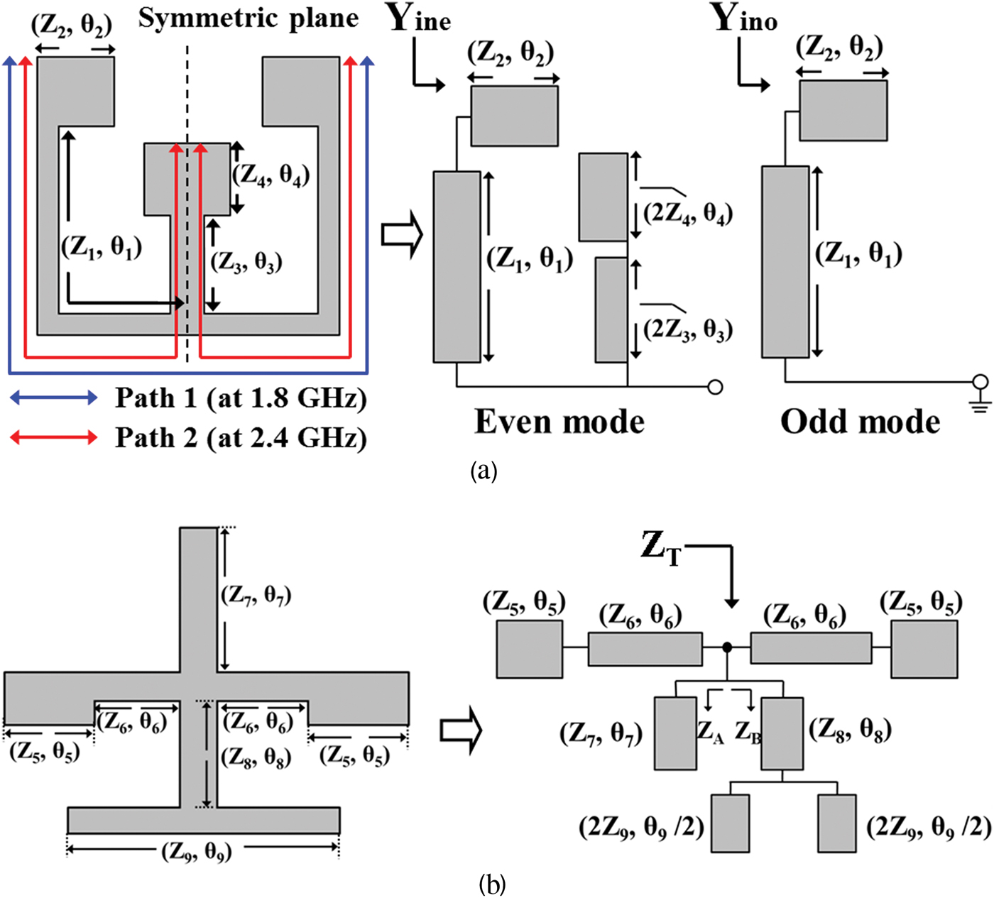
Fig. 2. Equivalent transmission line model of the (a) embedded SIR and (b) stub-loaded SIR (Z 1 = 131 Ω, θ 1 = 75°, Z 2 = 63 Ω, θ 2 = 5°, Z 3 = 115 Ω, θ 3 = 22°, Z 4 = 68 Ω, θ 4 = 20°, Z 5 = 88 Ω, θ 5 = 35°, Z 6 = Z 7 = Z 8 = 115 Ω, θ 6 = 33°, θ 7 = 75°, θ 8 = 27°, Z 9 = 84 Ω, and θ 9 = 66° in this work).
Letting Z A or Z B equal to zero, the stub-loaded SIR can be considered as a short circuit (Z T = 0 at zero frequency). The transmission zeros can be well determined.
Figure 3 shows the relations between the normalized f i /f 0 versus length ratio α 1 and α 2 with impedance ratio K 1 and K 2 and α 1 with r (=2θ S /θ T ) of the proposed resonators. In Fig. 3, paths 1 and 3 show the resonant modes of the conventional half-wavelength SIR and determined by SIR impedance and length ratios. For the path 2, the even- and odd-modes of the embedded SIR are corresponded to [f 2/f 0, f 4/f 0] and [f 1/f 0, f 3/f 0], respectively. To simplify the design, the parameters of the sections of [(Z 1, θ 1), (Z 2, θ 2)] are fixed, only to change the ratio r. It is found that even mode (f 2/f 0) can be designed very close to odd mode (f 1/f 0), while r = 0.5 with α 1 equal to about 0.1 or 0.9. Using the proposed embedded SIR, the even modes can be tuned within very wide frequency range and without affecting the odd modes. Therefore, the design of multi-band filters with very close passbands can be easily achieved and having a high isolation between the passbands.

Fig. 3. Relations between the normalized f i /f 0 versus length ratio α 1 and α 2 with different impedance ratio K 1 and K 2 and α 1 with r (=2θ S /θ T ) of the proposed resonators (K 1 = Z 2/Z 1, K 2 = Z 5/Z 6, α 1 = θ 2/(θ 1 + θ 2), α 2 = θ 5/(θ 5 + θ 6), θ S = θ 3 + θ 4, and θ T = 2(θ 1 + θ 2)).
B) Transmission zeros of the embedded SIR on the top layer
For the filter design, the center frequencies and fractional bandwidths (FBW) are f 1 = 1.8 GHz, f 2 = 2.4 GHz, and f 3 = 3.5 GHz with Δ1 = 22%, Δ2 = 8%, and Δ3 = 6%, respectively. The filter is designed and fabricated on the substrate of Duroid 5880 with dielectric constant ε r = 2.2, loss tangent tan δ = 0.0009, and thickness h 1 = h 2 = 0.787 mm. The passband ripples set as 0.01 dB. On the top layer of the proposed filter, the transmission zeros at the edges of 1st passband (1.8 GHz) and 2nd passband (2.4 GHz) can be controlled by the coupling path as M SL , resulting in the cross-coupling effects, as shown in Fig. 1(a). The corresponding (n + 2) × (n + 2) coupling matrix (n = number of resonators) can be written as
 $$\lsqb M\rsqb = \left[\matrix{0 &M_{\rm S1} &M_{\rm S2} &0 &M_{\rm SL} \cr M_{\rm S1} &M_{11} &0 &M_{13} &0 \cr M_{\rm S2} &0 &M_{22} &0 &M_{\rm 2L} \cr 0 &M_{31} &0 &M_{33} &M_{\rm 3L} \cr M_{\rm SL} &0 &M_{\rm 2L} &M_{\rm 3L} &0} \right].$$
The terms M 11 and M 33 (embedded SIRs) and M 22 (stub-loaded SIR) show the susceptances of the three asynchronously tuned resonators in this work. The coupling between the source to the resonator 1 and the load to the resonator 3 are indicated as M S1 and M 3L . Once the coupling matrix [M] is determined, the S-parameters of transmission and reflection responses are expressed as [Reference Cameron, Kudsia and Mansour10]
 $$S_{21} = - 2j\lsqb A\rsqb _{n + 2\comma 1}^{-1}\comma$$
 $$S_{11} =1 + 2j \left[A \right]_{11}^{-1}\comma$$
where
 $$\lsqb A\rsqb = \lsqb M\rsqb + \Omega_L \lsqb U\rsqb - j\lsqb q\rsqb \comma$$
where [U] is an (n + 2) × (n + 2) identity matrix except for [U]11 = [U] n+2;n+2 = 0, [q] is an (n + 2) × (n + 2) zero matrix except for [q]11 = [q] n+2; n+2 = 1, Ω L denotes the frequency variable of the low-pass prototype and [A] ik −1 means the (i, k)-entry of the inverse matrix of [A]. In this work, the source–load coupling element of M SL (shown in equation (3)) shows the capacitive coupling characteristic.
 $$M_{SL} = \pm \displaystyle{ 1 - \sqrt{1 - \left\vert S_{21} \right\vert^2} \over \left\vert S_{21} \right\vert}.$$
The choice of a sign is rather relative, which would depend on the signs of other elements in the n + 2 general coupling matrix. The coupling matrix [M] I , [M] II , and [M] III can be obtained as follows:
 $$\eqalign{\lsqb M\rsqb ^I &= \left[\matrix{0 &0.745 &0.281 &0 &-0.032 \cr 0.745 &0.023 &0 &0.891 &0 \cr 0.281 &0 &0.639 &0 &0.281 \cr 0 &0.891 &0 &0.023 &0.745 \cr -0.032 &0 &0.281 &0.745 &0} \right]\comma \; \cr & \; {\rm for}\, {\rm path}\, 1\, {\rm at}\, 1. 8\, {\rm GHz\comma \; } \cr \lsqb M\rsqb ^{II}&= \left[\matrix{0 &0.745 &0.281 &0 &- 0.032 \cr 0.745 &0.012 &0 & 0.882 &0 \cr 0.281 &0 &0.468 &0 &0.281 \cr 0 &0.882 &0 &0.012 &0.745 \cr - 0.032 &0 &0.281 &0.745 &0} \right]\comma \; \cr & \; {\rm for}\, {\rm path}\, 2\, {\rm at}\, 2. 4\, {\rm GHz\comma \; } \cr \lsqb M\rsqb ^{III} &= \left[\matrix{0 &0.745 &0.281 &0 &- 0.032 \cr 0.745 &0.114 &0 & 0.798 &0 \cr 0.281 &0 &0.157 &0 &0.281 \cr 0 &0.798 &0 &0.114 &0.745 \cr -0.032 &0 &0.281 &0.745 &0} \right]\comma \; \cr &\; {\rm for}\, {\rm path}\, 3\, {\rm at}\, 3. 5\, {\rm GHz}.}$$
When M SL < 0, the transmission zeros of T Z1 and T Z2 for the 1st passband at 1.8 GHz and T Z3 and T Z4 for the 2nd passband at 2.4 GHz can be determined. Figure 4 shows the positions of the transmission zeros T Z1, T Z2, T Z3, and T Z4 under different source–load coupling strength by tuning L. When L is changed from 0 to 6 mm, the transmission zeros T Z1 and T Z3 are increased within about 0.3 GHz variation and T Z2 and T Z4 are decreased within about 0.2 GHz variation. The source–load coupling is resulting in the cross-coupling effects by the multi-path propagations between the resonators.

Fig. 4. The positions of the transmission zeros (T Z1, T Z2, T Z3, and T Z4) under different source–load coupling strength by tuning L.
The elements in matrixes [M] I and [M] II are values in the lowpass domain. In the BPF domain, the external quality factor (Q ext ) can be calculated from M S1 = M 3L [Reference Cameron, Kudsia and Mansour10]
 $$Q_{ext} = \displaystyle{1 \over \Delta \times M_{S1}^2}.$$
Likewise, the coupling coefficients k ij between resonators i and j can be calculated by
 $$k_{ij} = M_{ij} \times \Delta.$$
Figure 5 shows the relations between the coupling coefficients K 13 I , K 13 II and external quality factor Q ext under changing the coupling space S. When coupling space S is increased, the coupling coefficients of K 13 I and K 13 II are decreased due to the coupling strength between the resonators is becoming lower. Based on the matrixes of [M] I and [M] II , the coupling coefficients in the dual-passband domain K 13 I (=K 31 I ) = 0.196, K 13 II (=K 31 II ) = 0.066, and Q ext = 4.54 are dominated.
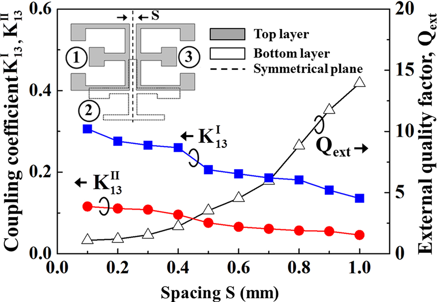
Fig. 5. Relations between the coupling coefficient K 13 I , K 13 II , and external quality factor Qext under changing the coupling space S.
C) Transmission zeros of the stub-loaded SIR on the bottom layer
The stub-loaded SIR is designed on the bottom layer along the symmetrical plane of the proposed filter. In Fig. 1(a), the coupling strength of path 3 (at 3.5 GHz) as M S2 and M L2 is almost constant by the limitation of the substrate thickness. Therefore, the transmission zeros T Z5 and T Z6 of the 3rd passband are controlled by tuning the structure parameters of the stub-loaded SIR. In Fig. 2(b), The ABCD matrix of the stub-loaded SIR can be obtained by
 $$\eqalign{\lsqb ABCD\rsqb _T &= \lsqb ABCD\rsqb _{SIR - left\, section} \times \lsqb ABCD\rsqb _{Stub}\cr &\quad \times \lsqb ABCD\rsqb _{SIR - right\, section}\comma \; }$$
where
 $$\eqalign{&\lsqb ABCD\rsqb _{SIR - left\, section} = \lsqb ABCD\rsqb _{SIR - right\, section} \cr & = \left[\matrix{\cos \!\theta_5 + \cos \!\theta_6 &j\lpar Z_5 \sin \!\theta_5 + Z_6 \sin \!\theta_6\rpar \cr j\lpar Y_5 \sin \!\theta_5 + Y_6 \sin \!\theta_6\rpar &\cos \!\theta_5 + \cos \!\theta_6} \right]\comma }$$
 $$\lsqb ABCD\rsqb _{Stub} = \left[\matrix{1 & 0 \cr 1/Z_T & 1} \right]\comma$$
where Z 0 = 50 Ω at the center frequency of 3.5 GHz. The transmission zeros occurs when S 21 = 0. The S 21 parameters are given by
 $$S_{21} = \displaystyle{- 2Y_{21} Y_ 0 \over \left(Y_0 + Y_{11} \right)\left(Y_0 + Y_{22} \right)- Y_{12} Y_{21}} = 0.$$
By transforming the matrix
 $\lsqb ABCD\rsqb _T \Rightarrow \lsqb Y_T \rsqb $
; therefore
$\lsqb ABCD\rsqb _T \Rightarrow \lsqb Y_T \rsqb $
; therefore
 $$Y_{ 21}=- \displaystyle{Z_T \over \matrix{\left(\cos \!\theta_5 + \cos \!\theta_6 \right)\left[j\left(1/Z_5 \sin \!\theta_5 + 1/Z_ 6 \sin \!\theta_6 \right)\right]\cr + \left[j\left(1/Z_5 \sin \!\theta_5 + 1/Z_ 6 \sin \!\theta_6 \right)\right]^2 \cr +\, \left[j\left(1/Z_5 \sin \!\theta_5 +1/Z_6 \sin \!\theta_6 \right)\right]\left(\cos \!\theta_5 + \cos \!\theta_6 \right)}}\comma$$
where Y 0 is the characteristic admittance. It is found that Y 21 = 0, which gives the conditions of the transmission zeros. In this work, we choose Z 5 = 88 Ω, θ 5 = 35°, Z 6 = Z 7 = Z 8 = 115 Ω, θ 6 = 33°, θ 7 = 75°, θ 8 = 27°, Z 9 = 84 Ω, and θ 9 = 66° for achieving the rejection level of transmission zeros better than 30 dB. Figures 6(a) and 6(b) show the relations between the image admittance (Im [Y 21]) and locations of the transmission zero T Z5 and T Z6 depending on the electrical lengths θ 7 and θ 8/θ 9. Changing the θ 8/θ 9 from 0.4 to 0.45, T Z5 is shifted from 3.37 to 3.3 GHz with maintaining of the T Z6. Similarly, changing the θ 7 from 67° to 75° (12.1 to 13.5 mm), T Z6 is shifted from 3.8 to 3.73 GHz. Figure 7 shows the current distribution and coupling paths of the proposed filter. It is clearly observed that the 1st and 2nd passbands (1.8/2.4 GHz) are generated by the embedded SIR with different paths and the 3rd passband (3.5 GHz) is generated by the stub-loaded SIR. Each passband can be implemented individually; therefore, low loss passband performance can be well achieved.

Fig. 6. (a) Relations between the image admittance (Im [Y 21]) and location of the transmission zeros and (b) the positions of the transmission zeros depending on the electrical lengths θ 7 and θ 8/θ 9 (where θ 9 is fixed as a constant of 66°).
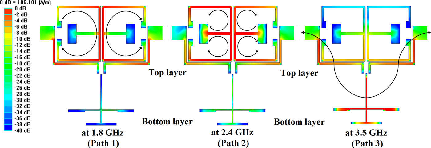
Fig. 7. Current distribution and coupling paths of the proposed filter.
In order to verify the passband arrangements, the S 21-magnitude of different (Z 3, θ 3) and the fundamental and spurious frequencies of each resonator are shown in Fig. 8. When the electrical length θ 3 increased from 22° to 35°, the 2nd passband is shifted to lower frequencies. The bandwidth of the 2nd passband can be modified by changing the section of characteristic impedance Z 3, as shown in Fig. 8(a). The fundamental and higher-order resonant modes of each resonator are shown in Fig. 8(b), where the higher-order resonant modes of each resonator can be blocked each other for obtaining the wide stopband range. To obtain the optimal triple-passband performance, the cross-coupling effect between the embedded SIRs and stub-loaded SIR is well achieved in Case 2, as shown in Fig. 9.
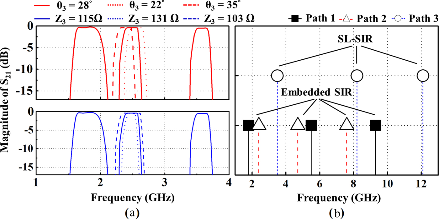
Fig. 8. (a) S 21-magnitude of different (Z 3, θ 3) and (b) the resonant modes of each resonator of the proposed filter.

Fig. 9. Simulated S 21-magnitude of the filter with different stub-loaded SIR arrangements.
III. RESULTS
The overall size of the fabricated filter is 30 × 25 mm2, i.e. approximately 0.27 λ g by 0.22 λ g , where λ g is the guided wavelength at the center frequency of the 1st passband. The proposed filter was measured by an HP 8510C vector network analyzer. The coupling strength between the input/output can be varied by tuning the length of the folded source–load lines. Figure 10 shows the photograph and measured results of the filter. The measured passbands have insertion losses of 0.42, 0.46, and 0.5 dB, return losses are 33, 22, and 28 dB corresponding to 1.8, 2.4, and 3.5 GHz, respectively. The 3-dB FBW are 22, 8, and 6%. The transmission zeros at each passband edge are clearly observed, resulting in high passband selectivity. The comparison of the proposed filter with other reported tri-band bandpass filters is summarized in Table 1. The multi-layered structure essentially helps not only to create the multi-path propagation, but also to reduce the overall circuit size.

Fig. 10. (a) Photograph and (b) measured results of the fabricated filter.
Table 1. Comparison of the proposed filter with other reported tri-band bandpass filters.

IV. CONCLUSION
In this paper, the new multi-layered triple-passband BPF is presented. The embedded and stub-loaded SIRs are utilized to obtain the triple-passband responses at 1.8/2.4/3.5 GHz. By controlling the impedance and length ratios of the embedded SIRs, the 1st and 2nd passbands can be easily determined. The stub-loaded SIR is designed to generate 3rd passband. The proposed filter can provide the multi-path propagation and generating the transmission zeros between the passbands by cross-coupling effects. The simple and effective design method of the triple-passband filter is useful for multi-band wireless communication systems.
ACKNOWLEDGEMENTS
This work was supported in part by the NSC under Grant numbers NSC 102-2633-E-168-001 and NSC 101-2622-E-168-021-CC3, and NSC 100-2221-E-006-040-MY2 and the LED Lighting Research Center of NCKU.
 Yung-Wei Chen was born in Taichung, Taiwan on August 1, 1989. He received the M.S. degree in Department of Computer and Communication, Kun Shan University, Tainan, Taiwan in 2013. He is now a Ph.D. student in Institute of Microelectronics, Department of Electrical Engineering, National Cheng Kung University, Tainan, Taiwan. He is the author and co-author of more than five papers in refereed journals and symposia proceedings. His research interests include analysis and design of passive microwave integrated circuits.
 Hung-Wei Wu was born in Taipei, Taiwan on October 28, 1978. He received the Ph.D. degree from Institute of Microelectronics, National Cheng Kung University, Taiwan in 2007. From October 2007, he joined the advanced optoelectronic technology center, National Cheng Kung University, Taiwan, where he is a Post-doctoral fellow. Now he is an Associate Professor in the Department of Computer and Communication, Kun Shan University. He is the author and co-author of more than 80 papers in refereed journals and symposia proceedings. His research interests include the design of planar microwave filter, thin-film microstrip line, transparent conducting oxide (TCO) thin films, RF biosensor and modeling of the electromagnetic bandgap structure equivalent circuits in microwave, and millimeter-wave communication applications.
 Yan-Kuin Su was born in Kaohsiung, Taiwan, on August 23, 1948. He received the B.S. and Ph.D. degrees in electrical engineering from National Cheng Kung University (NCKU), Tainan, Taiwan. Dr. Su is a member of SPIE, the Materials Research Society, and Phi Tau Phi. He received the Outstanding Research Professor Fellowship from the National Science Council (NSC), R.O.C., during 1986–1995. He also received the Best Teaching Professor Fellowship from the Ministry of Education, R.O.C., in 1992. In 1995, he received the Excellent Engineering Professor Fellowship from the Chinese Engineering Association. In 1996 and 1998, he received the Award from the Chinese Electrical Engineering Association. In 1998, he also received the Academy Member of Asia-Pacific Academy of Materials (APAM). In 2001, he was awarded as the Chair Professor by NCKU for his distinguished academic achievements. In 2007, he received the Awarding of Science Profession Medals by NSC, Taiwan, and was elected as the IEEE Fellow for his outstanding contribution to optoelectronics and nanophotonics research and education. Dr. Su is presently in charge of the Advanced Optoelectronic Technology Center (AOTC), NCKU and is also the president of Kun-Shan University, Tainan, Taiwan.


