I. INTRODUCTION
Power amplifiers (PAs) used in macro base stations have so far been realized with the aim of delivering high power (>50 W) [Reference Madan, Borran, Sampath, Bhushan, Khandekar and Tingfang1] in order to cover a wider area as possible for mobile phone communications. However, the wireless industry community is moving toward the realization of smaller base stations closer to the mobile users called “Pico” or “Femto” base stations [Reference Madan, Borran, Sampath, Bhushan, Khandekar and Tingfang1, Reference Debaillie, Giry, Gonzalez, Dussopt, Ferling and Giannini2]. Small base stations would deliver lower RF power with the consequent disadvantages of covering smaller area. This can however be overcome by placing a greater number of base stations in trafficked areas as in city centers and a minor number in non-trafficked areas as countryside. However, in order to perform the high-power-efficiency states also for the wideband spectrum frequency for the upcoming wireless communication standards new approaches must be considered. From here, dual-band/multiband [Reference Seung Hun, Choon Sik, Lee and Jaeheung3–Reference Chen11] and broadband [Reference Giofré, Colantonio and Giannini12–Reference Wu, Mkadem and Boumaiza14] PAs are in continuous development for RF/wireless applications. One approach that has been under attention in the last few years is called continuous modes [Reference Cripps, Tasker, Clarke, Lees and Benedikt15, Reference Carrubba, Clarke, Akmal, Benedikt, Tasker and Cripps16], which is related to the Class-J theory. Here by moving the fundamental drain impedance from its optimum point, it is possible to restore the high-power-efficiency state by proper adjustment of the higher harmonics.
This paper presents the design methodology and the realization of a reconfigurable dual-band PA at 2.1–2.2 and 2.6–2.7 GHz at high-power level of 30 W using the continuous/Class-ABJ approach [Reference Carrubba17]. The paper highlights the fact that thanks to the flexibility of the continuous-mode solutions broadband and multiband PAs can be easily realized with delivering high-power efficiency still satisfying the linearity requirement, both in a trade-off with bandwidth, of modern communication standards in now different targeted frequency bands. Furthermore, for the first time it will be seen that by matching the reactive Class-BJ solutions to the standard 50 Ω characteristic impedance, no matching degradation are in theory introduced.
II. THEORETICAL CLASS B/J/BJ MODES
This Section shortly explains in theory the difference between the standard Class-B [Reference Cripps18, Reference Colantonio, Giannini and Limiti19], the Class-J [Reference Cripps18, Reference Wright, Lees, Benedikt, Tasker and Cripps20], and Class-BJ PA modes for broadband operation [Reference Cripps, Tasker, Clarke, Lees and Benedikt15].
Equations (1) and (2) describe the Classes B/J/BJ current and voltage waveforms:
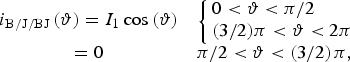 $$\matrix{ {i_{{\rm B/J/BJ}} \left(\vartheta \right)=I_1 \cos \left(\vartheta \right)} & {\left\{\matrix{0\lt \vartheta\lt \pi /2 \hfill \cr \lpar 3/2\rpar \pi\lt \vartheta\lt 2\pi \hfill} \right.} \cr {= 0} & {\pi / 2\lt \vartheta\lt \left({ 3/ 2} \right)\pi\comma \; } \cr }$$
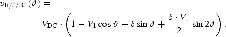 $$\eqalign{v_{{\rm B/J/BJ}} \left(\vartheta \right)&=\cr & V_{{\rm DC}} \cdot \left({1 - V_{1} \cos \vartheta - \delta \sin \vartheta+{\delta \cdot V_1 \over 2}\sin 2\vartheta}\right).}$$
Note that while the current waveform is supposed in theory to remain constant for the different modes, the voltage waveform varies as a function of δ. The classes B, J, and BJ voltage waveforms are achieved for δ = 0, δ = 1, and −1 < δ < 1, respectively. These new voltage waveforms named family of continuous voltage waveforms as well as the various impedances are displayed in Fig. 1.

Fig. 1. Theoretical Class-B/J/BJ current (blue) and voltage (red) waveforms for δ varying between −1 and 1 in steps of 0.2 (left figure); as well as fundamental and second harmonic terminations (right figure).
These new waveforms and therefore new solutions will all deliver the same power-efficiency performance. This is due to the fact that as noted from (2) the variation of δ will only vary the sin terms (imaginary parts) of fundamental and second harmonic voltage components. Therefore, being the cos terms (real parts) and the DC component constant, the power and the efficiency will be kept optimum invariant function of δ, as explained in details here [Reference Cripps, Tasker, Clarke, Lees and Benedikt15, Reference Carrubba, Clarke, Akmal, Benedikt, Tasker and Cripps16].
It is very important to highlight that the parameter δ has to vary between −1 and 1 in order to keep the voltage waveforms positive or grazing the zero value for δ = ±1 [Reference Cripps, Tasker, Clarke, Lees and Benedikt15]. If δ goes beyond that range, the voltage waveforms drop lower than zero, as highlighted in yellow in Figure 2 where δ = ±1.1, with consequently nonlinear behavior accompanied in reduction of power and efficiency.
Fig. 2. Theoretical Class-BJ voltage waveforms for δ = 0 (red line) and for δ = ±1.1 (green and blue lines).
Another aspect to take into account is the knee voltage V knee [Reference Cripps18, Reference Canning, Almuhaisen, Lees, Benedikt, Cripps and Tasker21]. Figure 3 shows the voltage and current waveforms as well as the load-lines for the Class-B mode when varying the knee voltage. Supposing a normalized fundamental voltage and current components both equal to 1, when V knee = 0 the ideal class-B case is presented with the half-wave rectified sinusoidal current waveform (blue trace) and the sinusoidal voltage waveform (red trace).
Fig. 3. Class-B voltage and current waveforms (left Fig.) and load-line (right Fig.) both function of V knee.
In the case V knee > 0, the current waveform I d will vary as a function of V knee, as shown in equation (3) [Reference Cripps18]:
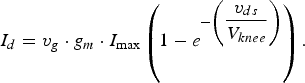 $$I_d=v_g \cdot g_m \cdot I_{\max } \left({1 - e^{ - \left({\displaystyle{{v_{ds} } \over {V_{knee} }}} \right)} } \right).$$
As also noted from Fig. 3, such current waveforms will present some troughs. This compression is due to the fact that in this case it is assumed that the voltage waveform remains constant sinusoidal (with V 1 = 1, where V MAX = 2 being V DC = 1). Therefore, when considering such V knee > 0, the minimum allowed voltage value where the device act as a current source is greater than zero. Therefore, with V knee > 0 and considering/enforcing the voltage to be sinusoidal (between 0 and 2 V) the device is enforced to go inside its knee/compression region (in this case to the minimum V = I = 0), as clearly shown in both plots of Fig. 3.
Figure 4 shows the efficiency behavior function of the knee voltage under the previous assumption. For V knee = 0 the standard efficiency value of 78.5% is obtained. When increasing the V knee to 0.1 V the efficiency decreases to about 68%. Increasing such V knee value it can be seen that the efficiency decreases, dropping down to about 64% for V knee equal to 0.2 V.
Fig. 4. Class-B efficiency function of the knee voltage.
III. MATCHING THE REACTIVE CLASS-J LOAD TO 50 Ω
In the literature review [Reference Pozar22], it is shown how to match a real impedance R S to another real impedance R L (i.e. R L = 50 Ω) using different networks and techniques, for example RLC networks or transmission/μstrip lines [Reference Pozar22].
In this paragraph, it will be seen in theory how to match a reactive source impedance
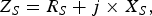 $$Z_S=R_S+ j \times X_{ S}\comma \;$$
where
 $$R_S=X_S$$
with the assumption of considering high-power transistors (i.e. 30 W) for which
 $$R_S \leq 25\, \Omega$$
to the environment system impedance of 50 Ω using a simple lossless LC low-pass filter network. Supposing to work at the device intrinsic plane, the aim of this paragraph is to show that when considering the Class-J reactive impedance, the matching of such solution to the characteristic impedance is not degraded compared with the standard real impedance case.
It is known [Reference Pozar22] that when the reactive part X S = 0, an LC low-pass filter (series-L and parallel-C and supposing a loss less network R = 0) can be used to match the input/source impedance (Z S) to the load impedance Z L = 50 Ω.
In this case
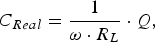 $$C_{Real}=\displaystyle{1 \over {\omega \cdot R_L }} \cdot Q\comma \;$$
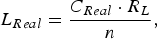 $$L_{Real}=\displaystyle{{C_{Real} \cdot R_L } \over n}\comma \;$$
where C Real and L Real are the values of the inductance and capacitance when considering only a real component. Where Q is the quality factor achievable by
 $$Q=\sqrt {n - 1}$$
and n is the ratio between the real part of the load impedance and the real part of the input/source impedance
 $$n=\displaystyle{{R_L } \over {R_S }}.$$
When considering the Class-J impedance in accordance with (4) and (5) and supposing R S ≤ 25 Ω (high-power device case), the parameters Q and n are equal to the previous case as well as the capacitor value will remain equal to (7) while the series inductor of (8) now termed L J will be
 $$L_J=L_{Real} - L_{ADD}\comma \;$$
where
 $$L{}_{ADD}=\displaystyle{{X_S } \over \omega }$$
is the addition inductance value due to the reactive Class-J load, with ω = 2 πf, where f is the operating frequency.
Figure 5 shows the C and L values function of the source resistance R S when X S = 0 and when R S = X S carried out at frequency F = 2.1 GHz in order to match the different impedances to the characteristic 50 Ω load. Noted that the capacitor C (red line) presents the same value for the two cases X S = 0 and X S = R S and it decreases when increasing R S. The inductor L presents different behavior for X S = 0 (blue line) and X S = R S (green line). For X S = 0 such inductor value needs to increase with increasing R S, while when considering the Class-J solutions X S = R S such L presents smaller values compared with case X S = 0 and it decreases with increasing R S. Between the solution X S = 0 (blue trace) and the Class-J extreme solution X S = R S (green trace) there are infinite solutions (intermediate continuous solutions) function of the parameter δ as explained in Section II. Varying the parameter δ the reactive part X S will vary and therefore in accordance with (12) L ADD will vary too leading to different L J in order to allow the matching condition. In both cases when X S = 0 and X S = R S, the parameter n remains constant (being n the ratio of the only real parts as stated in (10)) as well as the quality factor and they both decrease with increasing R S as shown in Fig. 6. This leads to the conclusion that for high-power devices (for the case where the fundamental load is less than 25 Ω) when matching the Class-J fundamental impedance (achieved at the device intrinsic plane) to the 50 Ω characteristic impedance using an LC network, or using more resonant networks depending of Q and R S, such reactive solutions do not degrade the matching quality compared with standard Class-B (only resistive) mode. Therefore, supposing to have a highly reflective second harmonic termination with the appropriate phase adjustment function of the reactive fundamental termination (in accordance with the Class-J theory), broadband PAs can be realized without output performance degradation due to the matching networks.
Fig. 5. Capacitance and inductance values function of R s when X s = 0.
Fig. 6. Q and n functions of R s.
IV. DUAL-BAND PA DESIGN STEPS – SIMULATIONS
A) Using the Class-ABJ theory for the realization of a reconfigurable dual-band power amplifier – considerations
The appropriate Class-ABJ impedance terminations can be presented by designing the appropriate output matching network (OMN). However, it is known that in practical PA implementation, the realization of such networks following the load traces of Fig. 1 for both fundamental and second harmonic impedances in a simultaneous way is challenging. This becomes more challenging when dealing with very high-power devices for which the fundamental optimum impedance is near to the short-circuit point. Furthermore, the analysis presented in the previous section has shown the right impedances to present at the intrinsic device plane thus frequency independent. When shifting it at the extrinsic plane thus dealing with packaged devices the right impedances must obviously be presented at the package plane and thus frequency dependent. Previous works have shown very well-performed broadband Class-BJ or continuous PAs [Reference Wright, Lees, Benedikt, Tasker and Cripps20, Reference Mimis, Morris, Bensmida and McGeehan23, Reference Carrubba, Lees, Benedikt, Tasker and Cripps24].
Another way to use the Class-BJ theory is to realize multiband PAs. In this paper, the continuous/Class-ABJ theory has been used to realize a reconfigurable dual-band PA working in the two frequency ranges 2.1–2.2 and 2.6–2.7 GHz. In a few words, the continuous Class-BJ approach has been applied in the overall frequency range 2.1–2.7 GHz, with focusing on the two extremes of the overall band. Therefore, during the design of the OMN, tedious simulations have been avoided in the middle band 2.2–2.5 GHz focusing and optimizing the two extreme targeted bands 2.1–2.2 and 2.6–2.7 GHz.
B) Class-AB simulations
The Class-ABJ PA has been designed using Computer-Aided Design (CAD) Advanced Design System (ADS) simulations and the accurate AlGaN/GaN power transistor model developed in [Reference Seelmann-Eggebert, Merkle, van Raay, Quay and Schlechtweg26] with gate width of 9.6 mm and gate length of 0.5 µm [Reference Damman25, Reference Seelmann-Eggebert, Merkle, van Raay, Quay and Schlechtweg26].
Before the Class-ABJ can be investigated/designed, the standard singular solution Class-AB mode must be achieved. At fundamental frequency F = 2.4 GHz and drain bias voltage V D = 40 V, by following the design procedure of [Reference Roff, Benedikt and Tasker27], input power, gate bias, and fundamental and second harmonic impedances are properly swept in order to achieve the best Class-AB trade-off between power, efficiency, and gain. Best performance is achieved for V G = −1.64 V, where I dq = 70 mA with the fundamental and second harmonic impedances as shown in Fig. 7(a). The harmonic impedances higher than two are considered short-circuited. Figure 7(b) shows the Class-AB output performance in terms of power, efficiency, and gain function of the input power sweep. Maximum drain efficiency (DE) of 64.9% with gain of 21.3 dB, while delivering 44.6 dBm of output power has been achieved.
Fig. 7. Simulated standard Class-AB DE, output power and gain function of the input power sweep.
C) Class-ABJ simulations
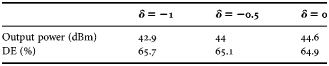
Once established the starting Class-AB state, the theory presented in Section II has been applied and the Class-ABJ performance has been carried out. The standard Class-AB mode achieved in previous Section is the δ = 0 solution of the Class-BJ mode. Therefore, by varying the parameter δ, various voltage waveforms (with maintaining a fixed current waveform) have been carried out leading to different load solutions as shown in Figs 8 and 9. Here the parameter δ has been varied in the range −1–0. The positive range (0–1) has initially not been taken into account due to stability considerations. Being the input transistor side still not optimized, at this stage the PA can present stability issues for some impedance terminations. Such issues have been overcome in the design of the input matching network (IMN) and the input bias network as then shown in Section IV D. The Class-ABJ fundamental and second harmonic impedances have been carried out at both intrinsic device plane and measurement plane, are shown in Fig. 8. The simulated Class-ABJ voltage and current waveforms are shown in Fig. 9, whereas the output power and DE function of δ are shown in Table 1. From such Table 1 it can be observed that when decreasing δ the power presents a 1.7 dB degradation from 44.6 to 42.9 dBm, while the efficiency presents some improvement from 64.9 to 65.7%.
Fig. 8. Simulated Class-ABJ Z F0 (blue) and Z 2F0 (red) carried out at both (a) intrinsic plane and (b) measurement plane for δ = −1, −0.5, and 0.
Fig. 9. Simulated Class-ABJ voltage (red) and current (blue) waveforms for δ varying between −1 and 0 in steps of 0.5.
Table 1. Output power and DE function of δ.
D) Class-ABJ output & input matching networks
Once the Class-ABJ fundamental and second harmonic terminations have been identified and the output performance satisfies the high-power efficiency target, the next stage is the actual OMN design. The design of the OMN is not an easy task for high-power devices due to the low optimum impedance (close to zero). This becomes more challenging for wide band frequencies. It is important to highlight again that in Section IV C, the various impedances (function of δ) have been carried out for the fixed frequency F = 2.4 GHz, while here the possibility of new impedance solutions (as shown in Fig. 8) allow to accommodate different optimum frequency solutions when designing the OMN. Therefore, with this approach, high-power efficiency and now broadband as well as multi-band PAs can be realized. The dual-band Class-ABJ OMN capable of synthesizing the impedances of Fig. 8 is shown in the schematic of Fig. 10, whereas Fig. 11 shows the S11 behavior (green trace) of the OMN of Fig. 10 as well as the target simulated impedances (red dots). Noted that for the fundamental impedances, which means for the two frequency ranges 2.1–2.2 and 2.6–2.7 GHz (highlighted in the zoomed window of Fig. 11), the simulated OMN S11 green trace fits properly with the targeted continuous mode impedance points whereas in the not of interest band (about 2.2–2.5 GHz) the green trace does not fit with the impedance (blue dot), as highlighted in the blue area. It is important to highlight that also the second harmonic loads have to be properly matched (in this case) around the edge of the Smith chart with the proper phases in accordance with the continuous mode theory.
Fig. 10. Reconfigurable dual-band Class-ABJ OMN schematic representation.
Fig. 11. Class-ABJ dual-and matching.
The last step of this approach is the design of the IMN in order to minimize the input reflection coefficient by conjugately matching the device input impedance Z IN ≈ 0.6-j2 (where Z IN presents a small phase variation function of the frequency) to the 50 Ω source load.
Figure 12 shows the zoomed IMN of the actual Class-ABJ PA photo (the photo of the overall PA is shown in Fig. 14). It can be noted that different resistors have been added for the circuit stabilization. The two resistors on the RF path are R1 = 5 Ω and R2 = 3 Ω. These two resistors have been accurately chosen as small as possible to minimize the gain loss. The resistors on the DC path R3 and R4 are respectively equal to 30 and 50 Ω. Thanks to such IMN design the PA results stable and it has shown about 4–5 dB gain improvement along the entire bandwidth.
Fig. 12. Reconfigurable dual-band Class-ABJ IMN photo.
Once the IMN is designed and thus the PA does not present stability issues, the overall PA can be studied and the output performance can be displayed.
The DE, power-added-efficiency (PAE), output power P OUT and the nonlinear gain (large signal gain) G are presented in Fig. 13 when driving the device with an input power Pin = 33 dBm corresponding to a compressing point of about 2–3 dB. Here the simulations show an average efficiency of about 64% in both the lower and the upper frequency bands 2.1–2.2 and 2.6–2.7 GHz, respectively. The low band presents a wider and smoother behavior, whereas the upper band presents a sharper behavior where the efficiency drops rapidly to low values at about 2.7 GHz. Both output power and gain are maintained >30 W and 11 dB in the two frequency bands. Note that despite the PA has been designed to work in the two bands 2.1–2.2 and 2.6–2.7 GHz, in the out-of-band frequency range 2.2–2.6 GHz the PA delivers P OUT > 20 W, DE > 31%, and G > 10 dB.
Fig. 13. Simulated DE (red), PAE (black), output power (blue), and gain (green) function of frequency.
It is important to highlight that such simulated power and efficiency (as well as then the experimental measurements presented in Section V) have been achieved in a reconfigurable mode, which means that when the low band is “On” the high band is “Off” and vice versa.
V. RECONFIGURABLE DUAL-BAND CLASS-ABJ PA FABRICATION AND RESULTS
After the theoretical and simulation analysis, the linear high-power efficiency Class-ABJ PA based on the AlGaN/GaN power transistor with gate width of W G = 9.6 mm (8 × 6 × 600 µm) and gate length of L G = 0.5 µm [Reference Damman25] has been realized as shown in Fig. 14. The PA has been fabricated on the Rogers substrate RO4003C with dielectric constant ε r = 3.3 and dielectric thickness of 0.51 mm.
Fig. 14. Photograph of the realized reconfigurable dual-band Class-ABJ PA and AlGaN/GaN powerbar.
A) CW measurements – efficiency, power and gain
Figure 15 shows the measured DE, PAE, output power, and gain behavior function of frequency when driving the PA with a CW stimulus where the input power is about 33.5 dBm in the frequency range 2.05 < F < 2.25 GHz and 32 dBm in the frequency range 2.45 < F < 2.6 GHz in order to deliver a constant average gain of about 10.5 dB. Here it can be noted that in the low-frequency band the PA behaviors as expected (from simulations) whereas for the upper frequency band the optimum performance is achieved at lower frequency compared with simulations. Now the optimum performance is obtained at about 2.45–2.6 GHz resulting in about 100 MHz shift (toward the low frequency) compared with the design simulations (2.6–2.7 GHz).
Fig. 15. Measured DE (red), PAE (black), output power (blue), and gain (green) function of frequency.
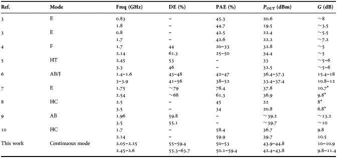
Both the output power and gain are maintained between 42.4 and 44.8 dBm and about 10–11 dB, respectively, in the bands 2.05–2.25 and 2.45–2.6 GHz. Furthermore, in both frequency bands the DE is maintained >55% whereas the PAE is >50%. Again, noted that the maximum DE and PAE are: 63.7 and 59.4%, respectively, achieved at 2.54 GHz, whereas the maximum output power is P OUT = 44.8 dBm revealed at F = 2.08 GHz. This Fig. 15 clearly shows that despite the design requirement was to optimize the power efficiency in the two requested bandwidths, using the Class-ABJ theory, the middle band (about 2.25–2.45 GHz) delivers almost constant output power and gain, whereas the DE is still above 40%, thus not presenting consistent degradations if compared with other different multiband designs as shown in the PAs dual-band State-of-the-Art of Table 2.
Table 2. State-of-the-art of dual-band PAs.
HT, harmonically tuned; HC, harmonically controlled.
*Calculated Gain having Pout and Pin; ~ estimated gain from the figures.
Figure 16 shows the Class-ABJ performance when driving the device in compression (about 2–3 dB compression) function of the drain bias voltage V D for the two frequencies F = 2.14 GHz (left Fig. 16) and F = 2.54 GHz (right Fig. 16). For F = 2.14 GHz both DE and PAE are constant at about 60 and 53%, respectively, for V D varying from 20 to 40 V in steps of 5 V. Here the gain is kept constant at about 9–10 dB, whereas the output power obviously increases with increasing V D from 40 to 44.7 dBm. For F = 2.54 GHz efficiency and PAE increase with increasing the drain voltage from 50 and 42%, respectively, to 63.7 and 60%. Here the gain also presents an increase with increasing V D from 7.5 to 11.6 dB.
Fig. 16. Measured DE, PAE, P OUT, and G for F = 2.14 GHz (left Fig.) and for F = 2.54 GHz (right Fig.) when varying the drain bias voltage V D between 20 and 40 V in steps of 5 V.
B) Measurements under Wideband Code Division Multiple Access (WCDMA) excitation
In this section, the Class-ABJ PA is studied when applying a 5 MHz WCDMA stimulus with 5.4 dB Peak-Average-Ratio (PAR). The output performance has been studied as a function of the input power as well as the drain bias voltage V D variations as shown in the contour plots of Fig. 17 for the frequency F = 2.14 GHz and in Fig. 18 for F = 2.54 GHz.
Fig. 17. Contour plots showing the measured average DE (left Fig.) and average gain (right Fig.) function of the average P OUT and V D at F = 2.14 GHz.
Fig. 18. Contour plots showing the measured average DE (left Fig.) and average gain (right Fig.) function of the average P OUT and V D at F = 2.54 GHz.
At F = 2.14 GHz (Fig. 17) the high-efficiency state (40–45%) is achieved for high output power (34–37 dBm) and low bias voltage V D (14–16 V). Such efficiency decreases when increasing V D; however, still DE values of about 30–32% are achieved at V D = 40 V, whereas delivering power of 36–38 dBm. This DE contour plot clearly shows that in order to maintain high-efficiency values when backing-off the power for the linearity requirement, the drain supply voltage should be decreased. Such behavior is typical of standard envelope tracking PAs [Reference Daehyun28]. The gain varies from about 13.6 dB down to about 9.5 dB (in compression) when decreasing V D.
At F = 2.54 GHz (Fig. 18), the PA shows the same DE behavior than low frequency. Noted that in this case the high-efficiency state is maintained for V D values up to 40 V where DE ≈ 42% whereas for the low frequency the PA has shown values of about 30–32% at V D = 40 V. For the gain parameter (right Fig. 18), the behavior is again similar to the low-frequency one, where in this case higher values can be achieved up to almost 15 dB in the linear region.
Figure 19 shows the adjacent channel power ratio (ACPR) Low results of the continuous/Class-ABJ PA function of the average output power at 2.14 and 2.54 GHz, respectively. The ACPR High are not shown being ACPR Low and ACPR High symmetrical. Such symmetry between the sidebands implies low memory effects and therefore the possibility of predistortability as it will be shown in Section V C.
Fig. 19. ACPR low function of the average output power for the two center frequencies F = 2.14 GHz (left Fig.) and F = 2.54 GHz (right Fig.).
The measurements have been carried out by driving the PA with the same 5 MHz WCDMA signal with V GS = −1.64 V and when varying the drain bias voltage V D from 14 to 40 V. Such ACPR behavior clearly shows that for both frequencies better linearity performance is achieved for high bias voltage V D with lowest ACPR (where delivering high power) values of about −47 dBc at 2.14 GHz delivering P OUT ≈ 37–38 dBm and about −42 dBc at 2.54 GHz delivering P OUT ≈ 36–37 dBm.
Despite the ACPR values do not reach −45 dBc (which is the required ACPR value for a 5 MHz signal) for some V D values for both frequencies; it is important to remind that such output performance is revealed without applying any predistortion technique. It will be seen in the next section that when applying a digital predistortion digital predistortion (DPD), the overall linearity is improved.
C) DPD and reconfigurable dual-band Class-ABJ frequency spectrum
The linearity requirement can be reached by decreasing the input stimulus as well as by applying different linearization techniques [Reference Kenington29]. In this case, for the improvement of the PA linearity, a general DPD technique is used. The linearization approach is based on the assumption that the nonlinear transfer characteristic of the RF amplifier can be described by the following equivalent baseband function:
 $$y=x \cdot \Gamma _{PA} \lpar \vert x\vert \rpar \comma \;$$
where ΓPA(|x|) represents the non-linear AM–AM and AM–PM transfer characteristic of the amplifier, depending on the input signal magnitude. The complex envelopes of the RF input and output signal are expressed by x and y, respectively. Introducing ΓPD(|x|) as the complex baseband predistorter gain, depending on the input signal magnitude, and isolating the real PA gain as M, it can be described as follows:
 $$y=x \cdot \Gamma _{PD} \lpar \vert x\vert \rpar \cdot \Gamma _{PA} \lpar \vert x\vert \rpar \cdot M.$$
From (14) it follows that ideal linearization will be achieved when ΓPD(|x|)·ΓPA(|x|) = 1 for all input signal magnitudes which means that ΓPD(|x|) describes the inverse of the amplifiers nonlinearities.
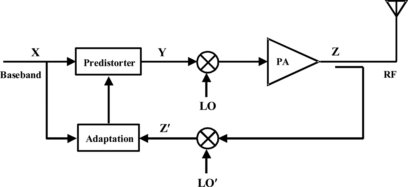
Figure 20 shows schematically the digital predistortion system including the frequency conversion. The inverse transfer characteristic is built by the predistorter. This system includes the measurement path, which is required for instantaneous control of the PA output.
Fig. 20. Adaptive digital predistortion system.
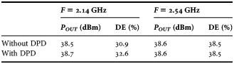
Such predistortion technique has been applied to the Class-ABJ PA with the spectrum contents shown in Fig. 21 for both frequencies 2.14 and 2.54 GHz with (w) and without (w/o) the use of the predistorter. In both the cases, w and w/o the use of the DPD and as mentioned previously, the PA shows a symmetric behavior in the two sidebands leading to almost the same ACPR values for the lower and upper ACP. For the low-frequency F = 2.14 GHz, when considering the PA w/o the use of any DPD an ACP of about −41 dBc is revealed. When applying the DPD, the linearity is considerably improved with ACP values of about −56. For the high-frequency F = 2.54 GHz, the values of ACP are about −34 and −50 dBc w/o and w the use of the DPD, respectively. Table 3 shows the PA output performance in terms of DE and P OUT again related to the PA behavior w and w/o the use of the DPD. Note that for F = 2.14 GHz the output power and DE before and after applying the DPD are quite close to each other. In the high band, F = 2.54 GHz both output power and DE are maintained perfectly constant.
Fig. 21. Spectrum with (blue trace) and without (black trace) applying the DPD at (a) F = 2.14 GHz and (b) F = 2.54 GHz.
Table 3. Class-ABJ Output Performance With and Without the use of DPD.
VI. CONCLUSION
This paper has presented the design steps and the physical realization of a reconfigurable dual-band 2.05–2.25 and 2.45–2.6 GHz single stage PA based on the continuous/Class-ABJ theory. The realized PA delivers efficiency >55% on both bands with maximum peak up to 63.7% as well as high output power >42.4 dBm with maximum peak value up to 44.8 dBm (30 W) under CW stimulus. Furthermore, the PA has shown satisfactory power efficiency and linearity performance when driving it with a 5 MHz WCDMA signal. Here, after applying DPD, the PA delivers an average efficiency of about 32 and 38.5% and average power of about 38.5 dBm with ACPR of −56 and −50 dBc at the centre frequency of the two bands 2.14 and 2.54 GHz, respectively. The results of the Class-ABJ PA have shown that by proper fundamental and harmonic impedance matching, a single-stage PA can deliver power and efficiency results comparable to the standard Class-AB but now for multiple frequency bands.
ACKNOWLEDGEMENT
This work was supported and funded by the German Federal Ministry of Economics and Technology under the IT2Green technology funding program, within the Intellispektrum project.
Vincenzo Carrubba (S’08, M’11) received the B.Sc. degree in electronic engineering and the M.Sc. degree in microelectronic engineering from the University of Catania, Catania, Italy, in 2005 and 2008, respectively.
From October 2008 to September 2011 he was with the Centre for High Frequency Engineering, Cardiff University, Cardiff, UK. Here, his Ph.D. research interests were the development of active load-pull techniques, the characterization of RF/microwave transistors, the investigation of broadband/continuous modes and the design of broadband power amplifiers.
He is currently working with the Fraunhofer Institute for Applied Solid-State Physics (IAF), Freiburg, Germany. Here his main interests include the design of high power-efficiency narrow band, multiband, and broadband power amplifiers, and efficiency-enhancement techniques.
Dr. Carrubba was the recipient of the European Microwave Prize at the 2012 European Microwave Conference (EuMC).
Stephan Maroldt received the Dipl.-Ing. degree in electrical engineering, with emphasis on microelectronics, from Technical University Ilmenau, Germany, in 2006. He received his doctoral degree in engineering (with honors) from University Freiburg, Germany, in 2010, in the field of novel GaN-based switch-mode power amplifier MMICs for mobile communications. Since 2008, he is research engineer with Fraunhofer Institute of Applied Solid-State Physics, Freiburg, Germany. His field of research covers design and technology for GaN HFET devices and GaN-based integrated and discrete circuits for applications in mobile communications, wireless transceivers, and radar in the microwave and millimeter-wave frequency range. His work is currently focused on advanced highly efficient switch-mode power amplifiers and multi-band transceivers for base stations.
Markus Mußer was born in 1974 in Villingen, Germany. He received the diploma (Dipl.Ing. (FH)) in Electrical Engineering in 2007 from the University of Applied Sciences Nuremberg, Germany. In 2007 he joined the RF Devices and Circuits Department of the Fraunhofer Institut of Applied Solid-State Physics in Freiburg, Germany, where he is currently working on GaN RF power bars and RF-high-power amplifiers.
Herbert Walcher received his Diploma degree and Dr. rer. nat. degree in 1977 respectively 1982 in Mineralogy/Crystallography from the Albert Ludwig University Freiburg. In 1982, he joined the Fraunhofer-Institut für angewandte Festkörperphysik, Freiburg, Germany. From 1982 to 1991, he was responsible for the preparation of bulk crystals of HgCdTe. From 1991 to 1993, he joined the diamond preparation group and from 1993 to 1998 the MBE group preparing layers for electronic and optoelectronic III/V semiconductor devices. His current research interest includes module assembly in the frequency range up to 110 GHz as well as high-voltage, high-power devices.
Friedbert van Raay received the Dipl.Ing. degree in electrical engineering from the Technical University of Aachen, Aachen, Germany, in 1984, and the Dr.-Ing. degree from the University of Kassel, Kassel, Germany, in 1990. From 1992 to 1995, he was with SICAN GmbH, Hannover, Germany, where he was involved with RF system development and measurement techniques. In 1995, he returned to the University of Kassel, as a Senior Engineer, where he supervised the Microwave Group, Institute of High Frequency Engineering. In November 2001, he joined the Fraunhofer Institute of Applied Solid-State Physics (IAF), Freiburg, Germany, as a Supervisor of the Device Modeling Group. His current research interests are development and characterization of high-speed digital and high-power millimeter-wave GaAs and GaN devices and circuits.
Rüdiger Quay (M’01, SM’10) was born in Köln, Germany, in 1971. He received the Diploma degree in physics from Rheinisch-Westfälische Technische Hochschule (RWTH), Aachen, Germany, in 1997, and a second Diploma in economics in 2003. He received his doctoral degree in technical sciences (with honors) from the Technische Universität Wien, Vienna, Austria in 2001, and in 2009 he received the venia legendi (habilitation) in microelectronics, again from the Technische Universität Wien. He is currently leader of RF-devices and circuit characterization group, and deputy head of the business field Gallium RF-power electronics with the Fraunhofer Institute of Applied Solid-State Physics Freiburg, Germany. He has authored and coauthored over 150 refereed publications and two monographs. Dr. Quay is chairman of MTT-6, Microwave and Millimeter Wave Integrated Circuits.
Oliver Ambacher received the Dipl.-Phys. and Dr. degrees (with honors) from the Ludwig-Maximilians and Technical University Munich, Munich, Germany, in 1989 and 1993, respectively. In 1993, he joined the Walter Schottky Institute, Technical University Munch, to investigate the epitaxial growth of group-III nitrides-based heterostructures. Since 1995, the research of his group has focused on fabrication of GaN-based devices as well as on the understanding of polarization-induced effects in group-III nitride heterostructures and quantum wells. During 1998–1999, he spent 1 year at Cornell University, Ithaca, NY, as an Alexander von Humboldt Fellow, where he was involved in the optimization of polarization induced AlGaN/GaN HEMTs for high-frequency and high-power applications. He became a Professor of Nanotechnology and head of the Institute for Solid State Electronics located at the Technical University of Ilmenau, Ilmenau, Germany, in 2002. In 2004 he was elected as head of the new Center of Micro- and Nanotechnologies. Since 2007 he has been the Director of the Fraunhofer Institute for Applied Solid State Physics (IAF), Freiburg, Germany, and Professor for Compound Semiconductor Microsystems with the University of Freiburg, Freiburg.
Dirk Wiegner is a member of technical staff in the Bell Labs Department Narrow/Broadband RF Transceivers/Amplifiers of the Wireless Access Research Domain in Stuttgart, Germany.
He received the Dipl.-Ing. degree in electrical engineering in 2001 at the University of Stuttgart, Germany.
At Alcatel-Lucent he was first engaged in characterization and modeling of SiGe and BiCMOS devices as well as in investigation of AlGaN/GaN HEMT technology for multibandpower amplifiers, within the microelectronics research department. In 2006, he changed to the Narrow/Broadband RF Transceivers/Amplifiers Department where he firstly continued working on highly efficient power amplifier concepts and technologies as well as on multiband and multi-standard capable amplifier solutions. Meanwhile, his work extended to analogue transceiver topics, including power amplifier.
Ulrich Seyfried, born in 1953 in Michelstadt/Odenwald, received his diploma in Physical Techniques at FH Wiesbaden in 1977. After military services he joined SEL in 1978, where he first worked in applications for electrical switches. In 1979 he changed to the Research Centre, with works in applications for piezo ceramics and development of fiber optics for 13 years. During 1992–2003, he worked in parameter extraction and modeling of semiconductor devices. Since 2004 he is working in the development of GaN RF-amplifiers.
Thomas Bohn is a member of technical staff in the Narrow/Broadband RF Transceiver/Amplifier Department within the Bell Labs Wireless Access Research Domain in Stuttgart, Germany. He received his Dipl.-Ing. degree in electrical engineering at the Chemnitz University of Technology, Germany.
At Alcatel-Lucent he is working on base stations for mobile telecommunication, focusing on research and implementation of digital algorithms for transceivers, especially for power amplifier linearization.
He contributed to several research projects in the past and recently to the award winning FP7 project “Earth”.
Andreas Pascht is head of the Narrow/Broadband RF Transceiver/Amplifier Department within the Bell Labs Wireless Access Research Domain in Stuttgart, Germany. The department is dealing with signal conditioning issues, transceiver architectures, and power amplification concepts for narrowband and broadband transceiver solutions. He received the Dipl.-Ing. and the Ph.D. degree in electrical engineering at the University of Stuttgart, Germany. Dr. Pascht's early work at Alcatel-Lucent included leading a transceiver team in the wireless area. Following that, he led the technology research for an internal venture for software-defined radio.
After transferring these results into the business group, he became unit manager for transceiver topics within the wireless research organization. The main focus is the Light Radio Project with the Cube as a compact transceiver solution.