I. INTRODUCTION
Thermoelectric (TE) materials are of interest for exploiting heat gradients to produce electricity by the Seebeck effect (Seebeck, Reference Seebeck1826; Oersted, Reference Oersted1823; Peltier, Reference Peltier1834). The efficiency of the devices depends on several factors, among which the figure of merit zT = S 2T/(ρk) , where S, ρ, T, and k are, respectively, Seebeck coefficient, electrical resistivity, absolute temperature, and thermal conductivity of the TE material (Rowe, Reference Rowe2012; Yang et al., Reference Yang, Jauregui, Zhang, Chen and Wu2012; Liu et al., Reference Liu, Zheng, Huang, He, Ao, Pan and Li2015; Zeier, Reference Zeier2017). To date, best commercial devices are based on Bi2Te3 alloys, reaching zT ≈ 1, while to be competitive TE devices should improve their performance by several times, up to zT = 4 (Yang et al., Reference Yang, Jauregui, Zhang, Chen and Wu2012). Looking for new high-zT TE materials and exploring effective methods to improve the performance of existing ones are critical issues.
Recently the attention of many research groups has focused on nanostructuring as a way to reduce the thermal conductivity of semiconducting TE materials: a higher density of boundaries appears to be beneficial because of the increase of phonon scattering (Poudel et al., Reference Poudel, Hao, Ma, Lan, Minnich, Yu, Yan, Wang, Muto, Vashaee, Chen, Liu, Dresselhaus, Chen and Ren2008; Xie et al., Reference Xie, Tang, Yan, Zhang and Tritt2009; Zhao et al., Reference Zhao, Yang, Cao, Mi, Zhang and Zhu2009; Rowe, Reference Rowe2012; Yang et al., Reference Yang, Jauregui, Zhang, Chen and Wu2012). Other approaches involve doping (Liu et al., Reference Liu, Zheng, Huang, He, Ao, Pan and Li2015), conducting fillers (Kumar et al., Reference Kumar, Ansari and Khare2018), ion substitution (Chmielowski et al., Reference Chmielowski, Bhattacharya, Jacob, Péré, Jacob, Moriya, Delatouche, Roussel, Madsen and Dennler2017), and crystal-structure engineering (Zeier, Reference Zeier2017) through 2D superlattices or quantum dots (Venkatasubramanian et al., Reference Venkatasubramanian, Siivola, Colpitts and O'Quinn2001; Yang et al., Reference Yang, Jauregui, Zhang, Chen and Wu2012). However, the challenge towards a wide application of TE devices requires a simple and low-cost fabrication process. Kesterite, made of earth-abundant and non-toxic elements (Cu2ZnSnS4, CZTS), is a promising TE material. The crystal structure is tetragonal, with space group I  $\bar{4}$, although recently an hexagonal P63mc polymorph has been chemically synthetized and vapour deposited as nanocrystalline CZTS (Azanza Ricardo et al., Reference Azanza Ricardo, Girardi, Cappelletto, D'Angelo, Ciancio, Carlino, Ricci, Malerba, Mittiga, Di Maggio and Scardi2015). Known so far for photovoltaic applications, kesterite for TE devices should work between 300 and 700 K (Yang et al., Reference Yang, Jauregui, Zhang, Chen and Wu2012; Kumar et al., Reference Kumar, Ansari and Khare2018), although economically competitive in the range from 600 to 800 K (Yang et al., Reference Yang, Jauregui, Zhang, Chen and Wu2012). As a p-type semiconductor (positive Seebeck coefficient) (Liu et al., Reference Liu, Zheng, Huang, He, Ao, Pan and Li2015), CZTS exhibits a remarkably low lattice thermal conductivity (from ~2 W/(m K) at 300 K to ~1 W/(m K) at 800 K), competitive with high-performance TE materials (Skelton et al., Reference Skelton, Jackson, Dimitrievska, Wallace and Walsh2015), but is disadvantaged by a low electrical conductivity (e.g. from ~2 S m−1 at 300 K to ~35 S m−1 at 700 K (Yang et al., Reference Yang, Jauregui, Zhang, Chen and Wu2012)). So far, zT values for CZTS nanocrystals range from around 4.6 × 10⁻⁵ at 300 K to around 0.026 at 700 K (Yang et al., Reference Yang, Jauregui, Zhang, Chen and Wu2012), while values of 0.36 at 700 K have been obtained for Cu-doped CZTS (Liu et al., Reference Liu, Huang, Chen and Chen2009). Ball milling is a common technique for the top-down production of TE materials (Rowe, Reference Rowe2012), where it is used to produce specific phases, by reactive milling (Azanza Ricardo et al., Reference Azanza Ricardo, Su, Müller and Scardi2013), as well as to grind the crystalline domains to the nanoscale in order to increase grain boundaries and introduce dislocations. Ball milled powders are then compacted by one of the many sintering techniques: spark plasma sintering (Liu et al., Reference Liu, Huang, Chen and Chen2009; Yang et al., Reference Yang, Jauregui, Zhang, Chen and Wu2012; Zhou et al., Reference Zhou, Shijimaya, Takahashi, Miyata, Mott, Koyano, Ohta, Akatsuka, Ono and Maenosono2017), hot-pressing (Yang et al., Reference Yang, Jauregui, Zhang, Chen and Wu2012; Devi Sharma and Neeleshwar, Reference Devi Sharma and Neeleshwar2018), cold-pressing, extrusion (Rowe, Reference Rowe2012).
In this work we present results of a preliminary study on nanostructured kesterite synthesized by reactive ball milling. XRD is used to follow the different stages of the milling process and sintering, showing the evolution of phases and microstructure. Preliminary results are shown on the TE behaviour.
II. EXPERIMENTAL PROCEDURE
CZTS powders were synthesized via reactive ball milling in a planetary mill (Fritsch P4 Pulverisette 4). An 80 ml brass jar was used with 25 brass balls (12 mm in diameter) as milling medium. The precursor materials (Cu powder, <75 µm, 99%; Zn powder, purum, 99%; Sn powder, puriss, 99%, S flakes, purum, 99.5%; all by SigmaAldrich) were weighted in exact stoichiometric quantity with a ball-to-powder weight ratio of 100:1, and milled with 250 µl of ethanol (99.8%, SigmaAldrich) as lubricant.
High energy milling conditions, from analogous research work (Broseghini et al., Reference Broseghini, Gelisio, D'Incau, Azanza Ricardo, Pugno and Scardi2016) were: jar rotation ω = −540 rpm, main disk revolution Ω = 300 rpm, for a fixed ratio ω / Ω = −1.8. Each milling operation was made in a single time interval of duration: 15, 30, 60, 90, and 180 min, respectively. The 60 min powder was used to make tablets with a cold-pressing machine manually operated with a load of 5 tons. The resulting shape was circular, with diameter 16 mm and thickness ~2 mm. The tablets were then sintered in Ar atmosphere with two different thermal treatments: TT1, 60 min at 300 °C (heating rate r = 20 K min−1) followed by 20 min at 560 °C (r = 20 K min−1 up to 520 °C and 10 K min−1 from 520 to 560 °C); TT2, 60 min at 400 °C (r = 20 K min−1) followed by 20 min at 660 °C (r = 20 K min−1 up to 620 °C, 10 K min−1 from 620 to 660 °C).
Powder and tablet specimens were characterized by XRD, collecting data at room temperature in a Rigaku PMG powder diffractometer, equipped with a graphite bent-crystal monochromator in the diffracted beam, using CuK α radiation generated at 40 kV and 30 mA. Scan range was from 8° to 82° (2θ), with a sampling step of 0.05° and a counting time of 10 s. TE characterizations have also been performed on the TT1 tablet specimen. Electrical resistivity and absolute Seebeck coefficient (with platinum standard) have been measured in the range from 40 to 400 °C while thermal diffusivity, in the range from 20 to 500 °C, has been determined with a Laser Flash (Linseis LZT-Meter combined LSR/LFA).
III. RESULTS AND DISCUSSION
The XRD patterns of ball-milled powders and tablets are shown in Figures 1 and 2, respectively, including details of the phase identification. The quantitative phase analysis was made with the Rietveld refinement software TOPAS, using a beta version 7 which supports the new macros based on Whole Powder Pattern Modelling (Scardi, Reference Scardi2008; Scardi and Leoni, Reference Scardi and Leoni2002) to refine the domain size in terms of a lognormal distribution of spheres (Scardi et al., Reference Scardi, Azanza Ricardo, Perez Demydenko and Coelho2018).
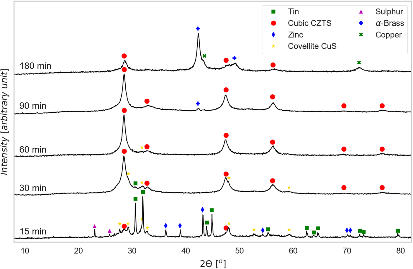
Figure 1. (Color online) XRD patterns of powders ball milled for increasing time, with indication of the identified phases [see text for details].

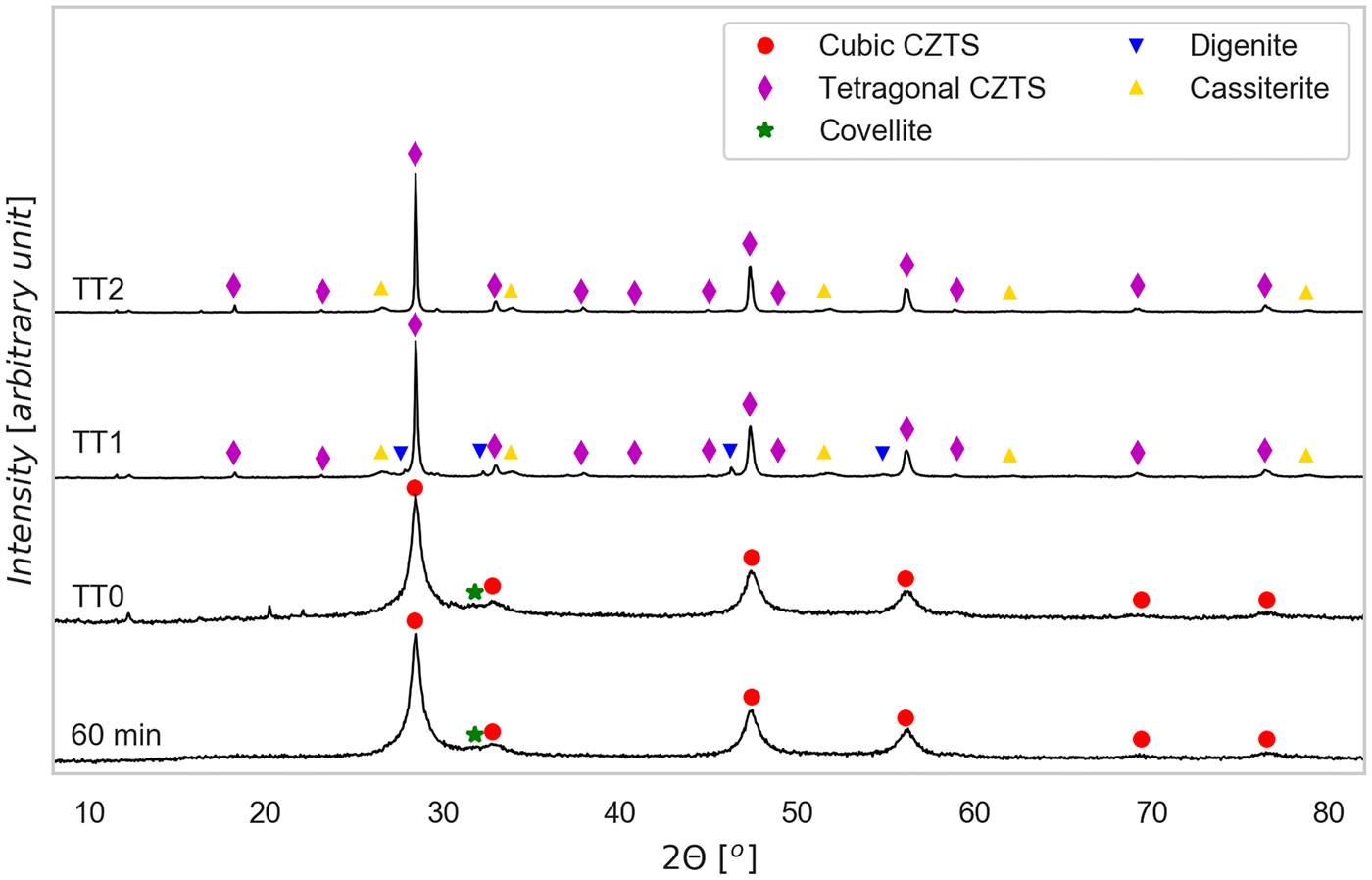
Figure 2. (Color online) XRD patterns of tablets, pressed only (TT0) and after heat treatments at 560 °C (TT1) and 660 °C (TT2), with indication of the identified phases. The XRD pattern of the powder ball milled for 60 min, used to produce the tablets, is shown again for easier comparison.
As shown qualitatively in Figure 1, evidence of the formation of CZTS is found since the shortest milling time, although the synthesis after 15 min is largely incomplete. The corresponding powder pattern shows peaks of all precursors (Sn, S, Zn, and Cu), and the intermediate sulfide phase covellite, CuS. At this stage CZTS is cubic, with a sphalerite (ZnS) structure, which is observed also for longer milling time. The XRD peaks of CZTS are visibly broader than those of the precursors, pointing out that the crystalline domains of the kesterite phase in formation are much smaller in size. Zinc sulfide, ZnS, might also be present, but cannot be confirmed as all peaks overlap with those of CZTS; however, based on stoichiometry and a simple mass balance, the main fraction is likely formed by a Sn-poor cubic CZTS. In fact, Sn appears for more than 80% in its precursor form, probably as a consequence of the large size of the Sn precursor particles, which is slower to react than the other metals.
The presence of precursors and intermediate phases decreases after longer milling. Starting from 30 min the CZTS fraction becomes the principal one, although a small amount of non-reacted Sn still appears, together with CuS. After 60 min milling, CZTS seems to be the main phase with CuS present just in minor amount <1.5% (from TOPAS refinement 1.3%, with an estimated standard deviation 0.6%). For longer milling times (90 min), precursors and intermediate phase disappear altogether, but traces of brass start to appear, to become the main phase in the powder ball milled for 180 min. This is because of the contamination of the powder from the vial and ball material, as the balls, after the completion of the reaction process, start eroding themselves and the vial.
As shown in Figure 2, the pressed only tablet presents no significant difference from the 60 min powder, whereas sintering changes both phase composition and microstructure. After heat treatment we observed a moderate growth of the CZTS crystalline domains, and formation of a minor fraction of impurity and precipitate phases. But the most striking difference with respect to the powders is the transition from cubic kesterite, with a sphalerite structure (space group F  $\bar{4}$ 3m), to the stable tetragonal form (space group I
  $\bar{4}$). Indeed, the last presents some extra reflections, most evident at ~18°, 23°, and 38°, which do not appear in the cubic phase (see the patterns of the 60 min powder and pressed only tablet). We attribute the formation of a cubic CZTS to stoichiometric deviations from the Cu2ZnSnS4 formula, and strong cation disorder caused by the high energy environment where kesterite forms during the reactive ball milling. On heating (TT1 and TT2), cations try to reach a more energetically stable configuration, thus leading to the cubic to tetragonal transition. This phase change involves a doubling of the c-axis (the CZTS tetragonal structure can be thought of as made of two cubic structures on top of each other), so that c = 2a. To the best of our knowledge stable CZTS in a cubic crystal arrangement at low temperatures has never been reported in the literature before.
Some authors have reported the existence of cubic CZTS, but at temperatures above 866 °C (Schorr and Gonzalez-Aviles, Reference Schorr and Gonzalez-Aviles2009; Schorr, Reference Schorr2011; Bosson et al., Reference Bosson, Birch, Halliday, Knight, Gibbs and Hatton2017). The difference is in the production methods, solution phase reaction (Yang et al., Reference Yang, Jauregui, Zhang, Chen and Wu2012), solid state reaction (Liu et al., Reference Liu, Huang, Chen and Chen2009), vapour deposition (Kumar et al., Reference Kumar, Ansari and Khare2017; Reference Kumar, Ansari and Khare2018), all involving a high-temperature step, whereas our procedure is at nominal room temperature.
Additional reflections in the tablet produced with TT1 are attributed to digenite, in the cubic (Cu7.2S4) or rhombohedral (Cu9S5) forms, and cassiterite, SnO2: the last phase likely originates from oxygen contamination. Despite the inert (Ar) atmosphere, residual oxygen encapsulated in the tablet during the powder pressing releases in the oven, thus reacting with the tablet material. This reaction path is supported also by the fact that the formation enthalpy of SnO2 is remarkably high, being reported to be -ΔHf298 = −577 kJ mol−1 (Cox et al., Reference Cox, Wagman and Medvedev1984). It is also possible to explain digenite formation as a side effect of partial Sn oxidation, which might have partly destabilized CZTS stoichiometry, leading to the formation of copper sulfides.
Extra peaks in the TT2 tablet pattern belong to SnO2, which is present in a lower amount than in the TT1 tablet: this explains the absence of digenite in TT2. It is also worth noting the sharpening of the CZTS peaks after the thermal treatments, pointing out a moderate but visible grain growth concurring to the cation ordering process discussed above. This picture is compatible with the known recrystallization temperature of CZTS, which has been reported to be around 400 °C (Guo et al., Reference Guo, Chen, Liu, Liu and Li2014), below the temperatures reached by TT1 and TT2.
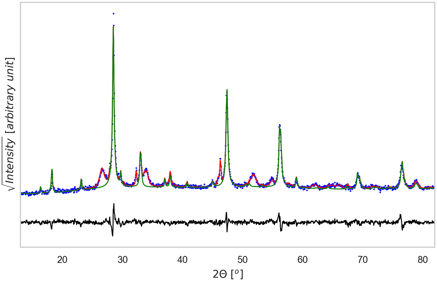
Sintered specimens appear to undergo a densification process, indeed the measured density at ambient temperature increases 10% after the thermal treatment, from ~3.08 g cm−3 to ~3.42 g cm−3 (geometrically measured on disk samples). By comparing this value with the mean-phase density calculated with TOPAS, being 4.98 g cm−3, we could estimate a porosity fraction of about 30%. Figures 3 and 4, show the results of TOPAS for the powder ground 60 min and the tablet sintered under TT1 condition. For all powder patterns, including that in Figure 3, CZTS was modelled with one or more sphaleritic (cubic) phases. This accounts for a possible multi-modality of the crystalline size distribution, and fluctuations in the CZTS stoichiometry. In this respect, however, inhomogeneous strain broadening (which has a characteristic trend with the 2θ angle, see Scardi et al. (Reference Scardi, Azanza Ricardo, Perez Demydenko and Coelho2018) and references therein) seems to be absent. This would rule out the presence of large fluctuations of stoichiometry, which also contribute to a line broadening which increases with the scattering vector modulus.
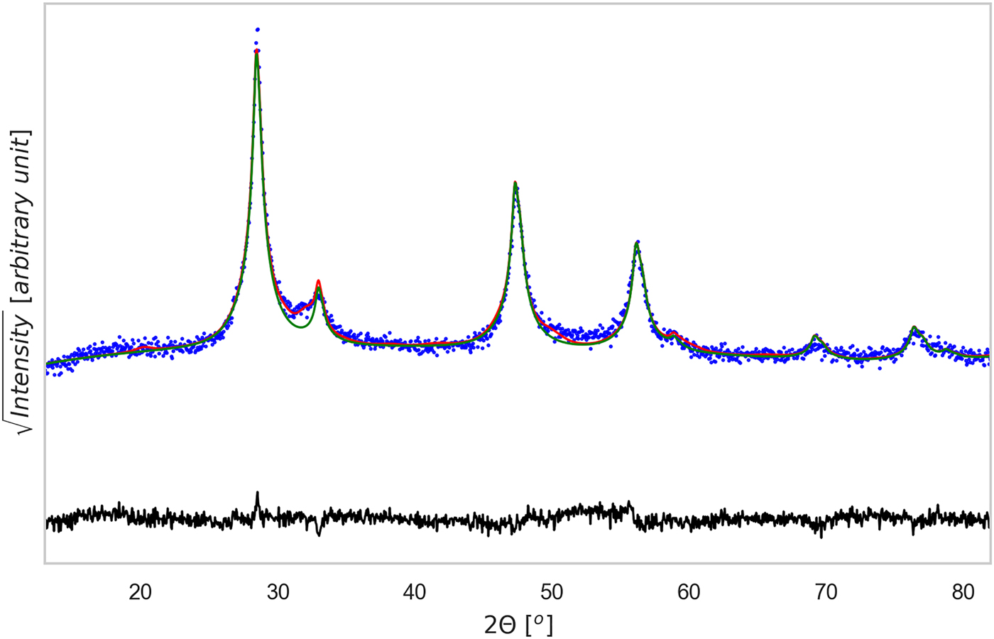
Figure 3. (Color online) XRD pattern refinement for the 60 min powder sample. Data were analyzed with Topas©, considering the phases identified in Figure 1. The CZTS phase is shown as a thin green line, whereas the difference between experimental data (dotted blue) and total model (solid red) is shown below (residual, solid black line). Rwp = 5.88, g.o.f. = 1.28, number of data points = 1481, number of fit parameters = 45.

Figure 4. (Color online) XRD pattern refinement for the TT1 tablet sample. Data were analyzed with Topas©, considering the phases identified in Figure 2. The CZTS phase is shown as a thin green line, whereas the difference between experimental data (dotted blue) and total model (solid red) is shown below (residual, solid black line). Rwp = 9.37, g.o.f. = 2.06, number of data points = 1481, number of fit parameters = 48.
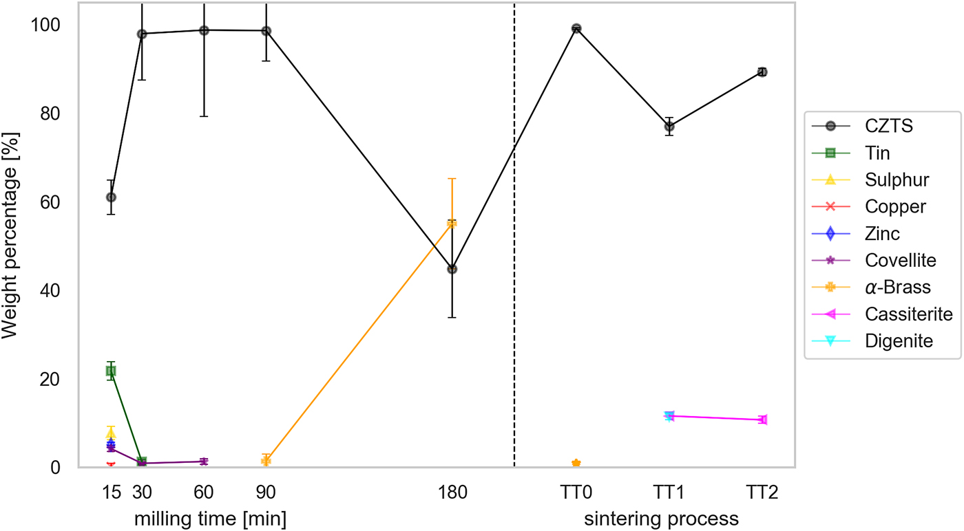
In the patterns of the sintered-tablet, CZTS can be modelled as a single phase with tetragonal structure. Therefore, for easier interpretation and comparison the model pattern of CZTS in Figure 3, it was represented as an only curve, even if made of more than one fraction. The main result, in fact, concerns the formation of CZTS: Figure 5 shows the trend of the CZTS weight fraction with the milling time and sintering temperatures of the tablets. CZTS reaches a maximum, with an almost pure phase between 30 and 90 min: the impurity fraction appears to be the lowest (<1.5%, in particular 1.3(6)%) after 60 min of milling.

Figure 5. (Color online) Weight percentages of CZTS and other phases in milled powders for increasing time and in the sintered tablets for increasing sintering temperature. [See text for details].
The mean domain size in the powder specimens ranges from 13 to 18 nm, while after sintering a limited grain growth occurs, to ~20 nm for TT1 and ~28 nm for the TT2 tablet. It seems therefore possible to obtain a solid component still preserving a fine nanostructure.
Figure 6 shows results of a preliminary characterization of the TE behavior made on one of the sintered tablets, TT1: more extensive tests are ongoing. Electrical resistivity ranges from ~8500 µΩ m at 40 °C to ~2000 µΩ m at 400 °C, showing a classical semiconducting behavior. The absolute Seebeck coefficient is positive, as expected for a p-type semiconductor, and ranges from ~40 µV K−1 at 40 °C to ~200 µV K−1 at 400 °C. The thermal diffusivity is ~0.006 cm2 s−1 at 20 °C and ~0.003 cm2 s−1 at 500 °C. Given the density of 3.418 g cm−3 (measured at ambient temperature) and a specific heat of 0.407 J/(g K) (calculated by considering a weighted average of all the present phases, including air in porosity, literature values for the specific heat of single components, and assuming it to be constant in temperature), it is possible to calculate the figure of merit zT for the kesterite TT1 tablet as ranging from ~9 × 10⁻⁵ at 40 °C to ~0.03 at 400 °C. These results are consistent with the literature (Liu et al., Reference Liu, Huang, Chen and Chen2009; Yang et al., Reference Yang, Jauregui, Zhang, Chen and Wu2012), but are remarkable for the low value of thermal diffusivity, which seems not to penalize the electrical resistivity. This could be because of the low density, so that air is trapped in the porosity and reduces the thermal diffusivity; nevertheless, porosity appears to have no relevant effect on the electron path, and indeed resistivity remains quite low (Liu et al., Reference Liu, Huang, Chen and Chen2009; Yang et al., Reference Yang, Jauregui, Zhang, Chen and Wu2012). Nano-size crystals, large grain boundary fraction, and stoichiometry disorder could also contribute to the low thermal diffusivity and electrical resistivity.
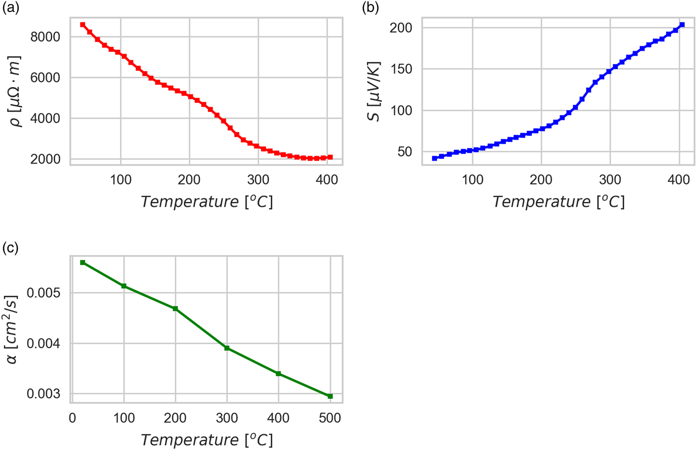
Figure 6. (Color online) Thermoelectric measurements of heat treated tablet TT1. Electrical resistivity (a), Seebeck coefficient (b) and thermal diffusivity (c) are reported as a function of the measurement temperature (each point is the average of three measurements with standard deviation within the size of the marker).
Further measurements and characterizations, including specific heat, are ongoing, in order to assess more accurately the material properties.
IV. CONCLUSION
When the elemental components of kesterite, Cu, Sn, Zn, and S, are mixed in stoichiometric proportions and ground together in a high energy planetary mill the ternary sulfide forms with relatively minor impurities, provided that milling does not extend to times sufficiently long to start eroding the brass vial and contaminating the resulting powder. CZTS forms fine grains (between 10 and 20 nm mean size) of a cubic polymorph, probably as an effect of a strong cation disorder. After sintering in temperature ranging from 560 to 660 °C the CZTS phase turns to the stable tetragonal form, with a minor growth of the crystalline domains, which are still rather fine. The sintered tablet shows remarkable TE properties, as the thermal diffusivity is rather low, while the electrical conductivity is not much depressed and the Seebeck coefficient is also reasonable and positive, as expected for a p-type semiconducting material like kesterite. The TE performance is good (zT is estimated as ranging from ~1 × 10⁻⁴ at 40 °C to ~0.03 at 400 °C), showing promising results in the studied temperature range.
ACKNOWLEDGEMENTS
This work was partly supported by the Italian Ministry of Economic Development in the framework of the Operating Agreement with ENEA for the Research on the Electric System; N. M. P. was supported by the European Commission under the Graphene Flagship Core 2 grant No. 785219 (WP14 “Composites”) and FET Proactive “Neurofibres” grant No. 732344 as well as by the Italian Ministry of Education, University and Research (MIUR), under the “Departments of Excellence” grant L. 232/2016 and ARS01-01384-PROSCAN grant. The authors would like to acknowledge also A. Mittiga of ENEA (Rome) for useful suggestions and discussions.