


I. INTRODUCTION
The role of compact antennas is increasing day by day due to rapid growth of wireless communications and microwave applications, which is supported by small-sized devices. For this purpose, antennas with broadband characteristics are in strong demand. In order to have good antenna performance, antennas having thick dielectric substrate with a low dielectric constant are preferred as they provide good efficiency, larger bandwidth, and better radiation characteristics. However, there exists a trade-off among the antenna performance, antenna size, and cost. Various methods are used in past to enhance the bandwidth, and improve the radiation characteristics of antennas and some of the techniques include increase of the substrate thickness [Reference Abdelaziz1, Reference Nishiyama and Aikawa2], the use of a low dielectric substrate, use of various impedance matching and feeding techniques, multiple resonators, and the use of slot antenna geometry [Reference Ali3–Reference Ansari and Ram5]. Also researchers have taken care to protect the microstrip patch antennas from adverse effects of dielectric and surface wave losses. One of the methods to mitigate such kinds of losses is to use defected ground structures (DGS). Recently, many patch antennas with DGS are suggested in various applications [Reference Liu, Li, Sun and Mao6, Reference Lin and Wang7]. DGS is realized by etching a defect in the ground plane of planar circuits and antennas. DGS is an etched periodic or non-periodic cascaded configuration defect in ground of a planar transmission line (e.g., microstrip, coplanar, and conductor-backed coplanar wave guide), which disturbs the shield current distribution in the ground plane because of the defects in the ground [Reference Weng, Guo, Shi and Chen8]. Owing to their excellent pass and rejection frequency band characteristics, DGS are chosen to be a part of patch antennas in order to improve their performances. Surface waves occur due to the trapping of total available radiated power along the surface of the antenna substrate. These waves reduce the antenna gain, efficiency, and bandwidth. All these problems can be evicted by using DGS structure in patch antenna, which supports wideband operation [Reference Liu, Li, Sun and Mao6, Reference Lin and Wang7].
The coplanar waveguide (CPW)-feeding mechanism has many advantages over microstrip-type feed lines, such as low dispersion, low radiation leakage, the ability to effectively control the characteristic impedance, and the ease of integration with active devices [Reference Dong, Zhang, Li and Fu9–Reference Simons17]. The purpose of this work is to enhance the gain of compact circular patch antenna using the specific strategy of DGS technique and compare it with the conventional patch antenna (without DGS).
II. CPW-FED BROADBAND ANTENNA ON FR4
Figure 1(a) shows the conventional CPW-fed circular patch antenna without DGS and Fig. 1(b) depicts the geometry of the proposed CPW-fed circular patch antenna with DGS. These patch antennas have equal cross-sectional areas. The width of the central strip of CPW antennas is of 3 mm, and the gap between the central strip and ground planes is 0.5 mm. There are two symmetric ground planes with dimensions of 7 mm × 8 mm lying on both side of the central strip. Figure 1(b) shows antenna with DGS of two circular slots etched of radius, “r 1 = 2.5 mm” each, in order to enhance the gain of the antenna. Since the antenna is made to design for higher frequencies for wireless and X-band applications, the size of the antenna is kept compact enough to fit the portable devices. The antenna is also fabricated on low cost “FR4” (flame retardant woven glass reinforced epoxy resin) substrate, which makes it cost-effective for various users.

Fig. 1. The geometric design of antennas (a) conventional CPW-fed circular patch antenna without DGS (b) proposed CPW-fed circular patch antenna with DGS.
The optimized design parameters obtained for the proposed patch antenna are L = 18 mm, W = 20 mm, g = 0.5 mm, W f = 3 mm, W g = 8 mm, L g = 7 mm, L f = 7.23 mm, r c = 5 mm, r 1 = r 2 = 2.5 mm, and r = 2 mm. Dielectric substrate (FR4 epoxy) has relative dielectric constant εr of 4.4, loss tangent of 0.02, and thickness “h” of 1.6 mm.
These antennas have a single-layer metallic structure on one side of the substrate (top) whereas the other side (bottom) is without any metallization. The circular disc is fed via CPW feed, which in turn is connected through a standard 50-Ω Sub Miniature Version A Connectors (SMA) connector. Figure 2 shows the fabricated patch antennas.
Fig. 2. The fabricated prototypes of antennas (a) conventional CPW fed circular patch antenna without DGS (b) proposed CPW-fed circular patch antenna with DGS.
III. DESIGN OF CIRCULAR MONOPOLE ANTENNA
The lower band edge frequency of a conventional circular printed monopole antenna with radius “r” can be evaluated from following equation [Reference Ray16]:
 $$f_{\rm l}=\displaystyle{{72} \over {\left({2r+{r \over 4}+p} \right)y}}{\rm GHz}.$$
Here, “y” is a factor accounting the role of dielectric material in reducing the lower band edge frequency by increasing the effective dimensions of the antenna and “p” is the gap between the circle and the ground plane, which is p = 0.23 mm in our case and y = 1.15 (for FR4). The lower band edge frequency with our design for r c = 5 mm comes out 5.45 GHz, which is near by the simulated and measured values.
The characteristic impedance of CPW line with finite-width ground plane on the FR4 dielectric substrate of height “h d” (see Fig. 3) is given by Simons [Reference Simons17]:
 $$Z_o=\displaystyle{{30\pi } \over {\sqrt {\varepsilon _{re} } }}\; \, \displaystyle{{K\lpar k\rpar } \over {K\lpar k^{\prime}\rpar }}\Omega \;.$$
Here, “K” is the complete elliptical integrals of first kind. The arguments k and k′ are dependent on the geometry of the CPW line
 $$k=\displaystyle{c \over b}\sqrt {\displaystyle{{b^2 - a^2 } \over {c^2 - a^2 }}} \, {\rm and}\, k^{\prime}=\sqrt {1 - k^2 }=\displaystyle{a \over b}\sqrt {\displaystyle{{c^2 - b^2 } \over {c^2 - a^2 }}}$$
and the effective dielectric constant (ε re) of the CPW line is given as
 $$\varepsilon _{re}=1+\displaystyle{1 \over 2}\lpar \varepsilon _r - 1\rpar \; \displaystyle{{K\lpar k\rpar } \over {K\lpar k^{\prime}\rpar }}\displaystyle{{K\lpar k^{\prime}_1 \rpar } \over {K\lpar k_1 \rpar }}.$$
Fig. 3. The CPW with finite dielectric height (h d) and finite ground planes.
Here,
 $$k_1=\displaystyle{{{\rm sinh}\left({\displaystyle{{\pi c} \over {2h_d }}} \right)} \over {{\rm sinh}\left({\displaystyle{{\pi b} \over {2h_d }}} \right)}}\; \sqrt {\displaystyle{{{\rm sinh}^2 \left({\displaystyle{{\pi b} \over {2h_d }}} \right)- {\rm sinh}^2 \left({\displaystyle{{\pi a} \over {2h_d }}} \right)} \over {\sinh ^2 \left({\displaystyle{{\pi c} \over {2h_d }}} \right)- {\rm sinh}^2 \left({\displaystyle{{\pi a} \over {2h_d }}} \right)}}}\comma$$
 $$\eqalign{k^{\prime}_1 &=\sqrt {1 - k^{\prime}_1 \; } \cr & =\displaystyle{{{\rm sinh}\left({\displaystyle{{\pi a} \over {2h_d }}} \right)} \over {{\rm sinh}\left({\displaystyle{{\pi b} \over {2h_d }}} \right)}}\; \sqrt {\displaystyle{{{\rm sinh}^2 \left({\displaystyle{{\pi c} \over {2h_d }}} \right)- {\rm sinh}^2 \left({\displaystyle{{\pi b} \over {2h_d }}} \right)} \over {\sinh ^2 \left({\displaystyle{{\pi c} \over {2h_d }}} \right)- {\rm sinh}^2 \left({\displaystyle{{\pi a} \over {2h_d }}} \right)}}}.}$$
These equations are used to ascertain the physical parameters of the proposed CPW designs and designed antennas are simulated using HFSS EM simulation software and results were verified in CST MWS. The CPW central metal strip width, length, and the gap (g) of the distance between the strip and the coplanar ground plane are fixed at 3, 7.23, and 0.5 mm, respectively, in order to achieve 50-Ω CPW feed line. The designed antenna with DGS has the circular patch of radius r c = 5 mm, which has a circular slot of radius 2 mm in the lower side of circular patch to enhance impedance bandwidth.
IV. RESULTS AND DISCUSSIONS
The broadband CPW-fed antennas with and without DGS are designed and simulated on HFSS and CST MWS. The fabricated antennas are characterized with Rohde and Schwarz vector network analyzer ZVA40 for reflection coefficient versus frequency, which has been compared with the simulated results in Fig. 4.
Fig. 4. Simulated and measured reflection coefficients of proposed antennas.
The simulated results of reflection coefficient versus frequency are in good agreement. The conventional CPW-fed antenna has huge impedance bandwidth but the gain is not significant for higher frequencies above 13 GHz. In the proposed antenna, we have introduced DGS in symmetrical ground planes. This proposed antenna as compared to conventional antenna achieves a significant impedance bandwidth of 100% ranging from 5 to 15 GHz with respect to the central frequency at 10 GHz. In literatures, we do not find improvement in radiation pattern characteristics in 12–15 GHz band for a compact design, as reported in this paper, as most of the works are limited to Ultra Wide Band (UWB) regions. The compact size and achieved broadband from 5 to 15 GHz make these antennas a good candidate for upper UWB applications and futuristic UWB as well.
We find a slight variation between the simulated and experimentally measured results at higher frequencies. This can be due to the dielectric losses introduced at high frequencies or uncertainty of the purchased dielectric constant of the substrate. In order to achieve a good impedance matching we need to optimize the gap between the radiating circular patch and ground plane [Reference Ray16]. Hence, we start analysis with varying length of the ground planes “L g” keeping all the parameters same. Figure 5 shows the effect of ground plane length on the proposed antenna with DGS. As per the simulated results most desired wideband is obtained at L g = 7 mm. For lower values lesser than 7 mm the antenna is not able to radiate properly for frequencies below 5 GHz and gives poor impedance matching. For value of L g >7 mm, i.e. 7.2 mm as shown in Figure 5, the antenna has no significant value of S 11. The parametric analysis is performed on the radii of the circular slots r 1 (see Fig. 6), which acts as DGS and change the current distribution in the ground plane of the patch antenna. This change in surface current distribution increases the gain of antenna at higher frequencies. From Fig. 7, it is found that optimum radius of the circular DGS is 2.5 mm, which gives broad impedance bandwidth as compared to 2 mm, whereas on increasing the value by 0.5 mm makes antenna non-resonating for 9.8–10.2 GHz band.
Fig. 5. Effect of variation of length of ground plane.
Fig. 6. Effect of the variation of radius of the circular slot “r 1” on ground plane (radius of DGS).
Fig. 7. Simulated result of the proposed antenna with various radii of main circular patch “r c” and “r”.
Figure 7 shows the results of parametric analysis performance on the radii “r” and “r c” to improve reflection coefficient versus frequency characteristics around 10 GHz. It is observed that when the radius of the circular slot “r” is 1 mm the impedance matching is poor and improves when it is increased to 2 mm. We have also found that the value of “r c” below 5 mm results in decrease in impedance bandwidth, while increasing its value for “r c” to 5.2 mm, results in poor impedance matching. Hence, we have opted the values of “r c” = 5 mm and “r” = 2 mm.
We have also analyzed the current distribution in the antenna at various frequencies, as shown in Fig. 8. The current value is high along central metallic strip of the CPW feed and lower edge of the main circular patch “r c” of the proposed antennas. In the ground planes, the current value is more on the upper edge near the circular patch “r c” (along the x-direction). This explains that the impedance matching of the antenna is also dependent on gap between CPW central feed strip and ground plane as well as gap between the upper edge of ground plane and patch. These gaps are very important parameter for proper signal coupling from feed line to patch. This explains the importance of optimized dimensions of the ground plane [Reference Ray16].
Fig. 8. Simulated current distributions of the proposed antennas at various frequencies: (a) antenna without DGS, (b) antenna with DGS.
Figure 9 shows the radiation patterns of the proposed antennas (CPW-fed antenna with and without DGS) at selective frequencies of 5, 8, 10.5, and 15 GHz, respectively.
Fig. 9. Stimulated radiation patterns of the proposed antennas (x–z plane, omnidirectional-H plane, and bidirectional-E plane) (a) without DGS (b) with DGS at four different frequencies.
From the radiation patterns shown in Figure 9, we see that gain and radiation characteristics of the proposed antenna with DGS have improved considerably as compared to conventional antenna (without DGS) at 15 GHz. The gain has increased to 7 dB and the H-plane radiation pattern has become nearly omnidirectional. At higher frequency, the ripple occurs in radiation pattern due to edge reflections.
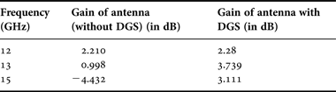
It is noted that the radiation patterns of the antenna with DGS in the H-plane (x–z plane) are nearly omnidirectional in entire band of 5–15 GHz and radiation patterns in the E-plane (y–z plane) resembles figure of eight and are bidirectional. Table 1 shows the comparison between peak gains of the conventional CPW-fed patch antenna and antenna with DGS at higher frequencies from 12 to 15 GHz. A significant improvement in gain is noticed with antenna having DGS. This is due to reduction of surface waves at these higher frequencies. Figure 10 shows the peak gain of the proposed antennas for the frequency band 5–15 GHz. Maximum gain of the antenna with DGS is 3.88 dB at 7 GHz. It can be seen that antenna with DGS has stable radiation patterns (see Figure 9) and achieves improved gain at higher frequencies (see Figure 10). The gain of the antenna is significantly high for practical applications.
Fig. 10. Peak gain of the proposed antennas.
Table 1. The peak gains of the proposed antennas at higher frequencies.
V. CONCLUSION
CPW-fed circular patch antenna has been designed, fabricated, parametrically analyzed, and characterized to obtain high gain with the defected ground structure. The antenna offers impedance bandwidth of 100% and gain enhancement in higher frequency ranges as compared to the conventional circular patch antenna. The wideband has been achieved by optimizing the dimensions of the ground planes and the radius of the slot “r” in circular patch. Inserting circular DGS of optimized radius in ground plane of conventional CPW-fed antenna has resulted in gain enhancement. The measured impedance bandwidth (VSWR < 2) of proposed antenna is 10 GHz. It covers the C, X, and upper UWB. The antenna offers gain improvement of 2.74 dB at 13 GHz and 7 dB at 15 GHz. The antenna design is simple and can be easily mounted and packaged with other microwave devices and circuits. The antenna has stable radiation pattern and high gain in entire band. The proposed antenna structure can be used for futuristic wireless systems.
ACKNOWLEDGEMENT
The authors are grateful to CEERI (CSIR), Pilani (Rajasthan) and Rajasthan University, Jaipur, India, for providing the facilities for this research work.
Kirti Vyas received an M.Tech. degree in Electronics and communication from the Malvia National Institute of Technology, Jaipur, Rajasthan, India. She is an M.Tech. coordinator at the Arya College of Engineering and I.T., Kukas, Jaipur, Rajasthan, India. She is pursuing her Ph.D. from Bhagwant University, Ajmer. Her main research interests are design and optimization of microstrip patch antennas.
Garima Sanyal is an M.Tech. Scholar in Electronics and Communication from Arya College of Engineering and I.T. and her fields of interest are design and optimization of planar antennas.
Dr. Arun kumar Sharma received his Ph.D. degree in 1984 from the Physics Department of University of Jodhpur, Rajasthan, India. From 1980 to 2010, he worked as a Scientist with Central Electronics Engineering Research Institute; Pilani, India for various R&D projects such as Power Triodes, Dispenser Cathodes, Surface Analysis by Auger Electron Spectroscopy, Thyratron, DBD-based VUV/UV sources, Terahertz sources. He has authored more than 90 research articles and his current research interests are in Terahertz Communication, Microwave filters, Microstrip Antennas, etc.
Prof. P.K. Singhal received his B.E. and Ph.D. degrees in Electronics Engineering from Jiwaji University, Gwalior (MP) India, in 1987 and 1997, respectively, and the M.Tech. degree in Microwave Electronics from the University of Delhi, India in 1989. Currently, he is working as a Professor, in the Department of Electronics Engineering, Madhav Institute of Technology and Science, Gwalior (MP), India. He has about more than 100 publications to his credit at the national and International level. His research interest includes electromagnetic, antennas, microwave circuits, and communication systems.


