I. INTRODUCTION
Magnetic nanowires, such as Co, Fe, and Ni, have been widely studied for their potential applications in electronic devices (Carignan et al., Reference Carignan, Yelon, Menard and Caloz2011; Zhang et al., Reference Zhang, Divan and Wang2011). A study on the magnetic properties of nanowires is very important for both the applications and the understanding of the mechanism of structural anisotropy of magnetic nanowires. A simple method for the synthesis of nanowire arrays is by using templates, such as an anodic aluminum oxide (AAO) template. Some effective methods have been put forward to fabricate nanowire arrays based on an AAO template. With an AAO template, magnetic metal nanowires can be synthesized by DC electrodeposition (Bentley et al., Reference Bentley, Farhoud, Ellis, Nickel, Lisensky and Crone2005). The magnetic anisotropy of nanowires results from two aspects. One is shape anisotropy due to a high aspect ratio and an ultra-small diameter of nanowires. The other is crystalline texture, which is commonly caused by the preferential growth of grains in pores of a template (Yin et al., Reference Yin, Li, Jian, Bennett and Xu2001). For example, Pan et al. (Reference Pan, Liu, Yi, Poh, Lim, Ding, Feng, Huan and Lin2005) studied the influence of deposition voltage and temperature on the orientation of Ni nanowires. They reported that single-crystalline Ni with the (110) orientation can be produced at high deposition potential and low temperature. Also Wang et al. (Reference Wang, Fei, Xu, Jin and Zhang2005) indicated that the preferential orientation of Ni nanowires is along the [110]-direction when the diameter of an AAO template is less than 70 nm, whereas nanowires grow along the [111]-direction when the diameter is larger than 90 nm.
It is important to control and characterize the texture and grain size because they can impact the performance of magnetic nanowires. Therefore, many researchers have investigated the influences of pH value, electric voltage, and temperature on the texture of magnetic nanowires. Beyond varying the plating parameters, applying a magnetic field during electrodeposition may be another route to control the preferred orientation, but the study on the effect of the magnetic field on the textured Ni nanowires prepared by electroplating has been limited. A magnetic field can supply extra energy to the nucleation and growth of magnetic metal nanowire and affect the textures of some magnetic nanowires.
Although the θ–2θ scan X-ray diffraction (XRD) method has been widely used to characterize the preferred orientation (or fiber texture) of a material, it is difficult to accurately measure the degree of preferred orientation. Among many XRD techniques, the ω-scan method is a simple and effective way to analyze the degree of fiber texture (Fei et al., Reference Fei, Liu, Ding, Li and Wang2009), where ω is the angle of the incident X-ray beam. Using Gaussian fitting of the ω-scan XRD curves, qualitative and quantitative characterization of fiber texture can be obtained.
In the present study, Ni nanowire arrays were prepared on AAO templates in different magnetic fields through the electroplating method. The effects of applied magnetic field on the texture and magnetic properties of Ni nanowire arrays have been investigated.
II. EXPERIMENTAL
The AAO templates used in our experiments are commercial nanoporous alumina membrane made by Whatman® Anodisc. A thin layer of Ag was sputtered onto one side of a template for conducting by using magneto sputtering technology. The DC electroplating pool used in the experiments is shown in Figure 1. A Ni flake (99.9%) was anodic, and the side of template with sputtered Ag was pressed onto the Cu tape using scotch tape. A magnetic field was applied during electroplating, which was provided by a square magnet with the dimension of 50 × 50 mm2, and the magnetic field (H p) was adjusted to the distance of the magnet surface to the sample, and the H p was adjusted from 0 to 2400 Oe.

Figure 1. Schematic diagram of the electroplating process.
The electrolyte used for Ni electrodeposition was composed of 0.38-M NiSO4, 0.13-M NiCl2, 0.65-M H3BO4, and 60-ppm CH3(CH2)11OSO3-Na, adjusted to pH 5.2 with a NaOH solution (Chu et al., Reference Chu, Wada, Inoue, Todoroki, Takahashi and Hono2002). Nickel electroplating was performed at 1.5 V and 30 °C for 20 min, and with mechanical stirring. Prior to the Ni electroplating, the specimens were immersed in the electrolyte and treated in an ultrasonic bath for 1 min to eliminate air in the pores of anodic alumina membrane. The sample is aligned normal to the surface of the magnet.
The crystal structure and the texture of the Ni nanowire arrays with AAO templates were studied using XRD methods on a Philips X'pert X-ray diffractometer with CuKα radiation at 40 kV and 40 mA. A scanning electronic microscope (SEM) was used to investigate the morphology of nanowires on a H-3000 SEM. The magnetic hysteresis loops of nanowires were measured by a vibrating sample magnetometer (VSM). The magnetic properties, including squareness, saturation field, and anisotropy, were derived from the hysteresis loops.
III. RESULTS AND DISCUSSION
A. Microstructure
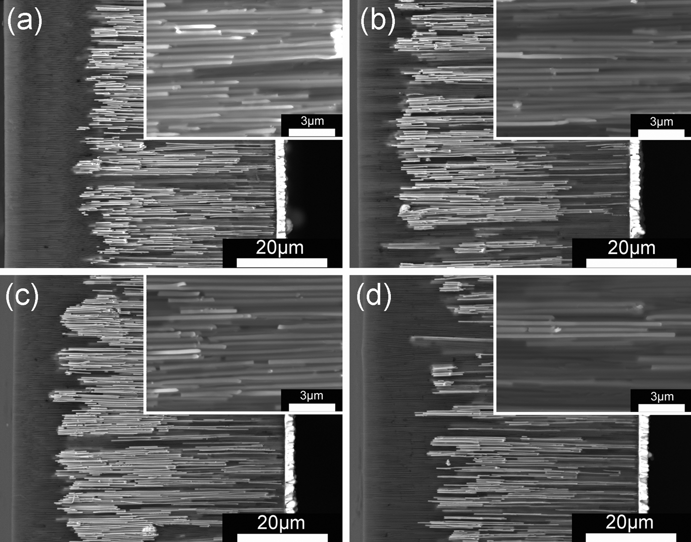
The SEM cross-section images, taken with the backscattering electronic (BSE) image model, of Ni nanowires embedded in an AAO template are shown in Figure 2. The bright wires are Ni nanowires because of a larger elemental number of Ni. The total length of the AAO template is about 60 µm. The nanowires deposited without a magnetic field are about 40 µm long. The nanowires deposited in a magnetic field are a little longer than that without a magnetic field (about 50 µm), which illustrates that the growth rate of Ni nanowires can be enhanced by a magnetic field. The insets of Figure 2 show the high-magnification SEM images of nanowires, which indicate that the diameter of nanowires is about 200 nm.
Figure 2. Backscattering electronic SEM images of Ni nanowires deposited in different magnetic fields applied during electroplating, with the insets being high-magnification images: (a) 0 Oe, (b) 600 Oe, (c) 1200 Oe, and (d) 2400 Oe.
Figure 3(a) shows the XRD patterns of Ni nanowires, in which the XRD intensities are normalized using the intensity of the strongest diffraction peak for a clear comparison. All samples show a sharp (220) peak and a small (111) peak of Ni, which suggests that the (110) texture exists in all Ni nanowire arrays, i.e. the Ni grains grow preferentially along the [110]-direction. The full-width at half-maximum (FWHM) values for (220) diffraction peaks for the nanowire arrays were obtained from step scans of the XRD peaks, and the results are shown in Figure 3(b). Generally, the smaller the FWHM of the XRD peak, the larger the grain size in the sample. The nanowire deposited in the 600-Oe magnetic field has the largest grain size. But when H p reaches 1200 Oe, the grain size is smaller than that of the nanowires plated without a magnetic field. Nanowires deposited in the 2400-Oe magnetic field have the smallest grain size.
Figure 3. θ–2θ scan XRD curves (a) and FWHM values (b) of the (220) diffraction peaks for Ni nanowires with different magnetic fields (H p) applied during electroplating.
B. Texture
To quantify the (110) texture formed in Ni nanowire arrays, ω-scan XRD measurements were carried out. The detector was fixed at the 2θ position of the (220) XRD peak, while the X-ray incidence angle (ω) scanned from 0 to 2θ. As shown in the previous study (Fei et al., Reference Fei, Liu, Ding, Li and Wang2009), the texture can be analyzed through ω-scan XRD curves. The ω-scan curves for Ni nanowire arrays deposited in different magnetic fields are shown in Figure 4. The peak positions of (220) ω-scan curves are located at θ 220, which further confirms that the texture in the nanowires is [110] (Fei et al., Reference Fei, Liu, Ding, Li and Wang2009). After Gaussian fitting, the integral width (w) of an ω-scan peak can be obtained. It is clear that the w value gives the diffusion degree of the texture, and a large w value corresponds to a weaker texture degree. Figure 4(e) shows the effect of an applied magnetic field in the electroplating process on the w value. It can be found that the effect of a magnetic field on the texture diffusion degree of Ni nanowires is not monotonic, and the smallest texture degree is obtained in the sample deposited at 600 Oe. But the (110) texture diffusion degree decreases slightly in the sample deposited at 2400 Oe. In addition, the (111) diffraction peak intensity is enhanced at a higher H p value as shown in Figure 3(a), which indicates that the (111)-oriented grain number is increased by a high magnetic field.
Figure 4. ω-scan XRD curves of (220) texture in nanowires deposited in different magnetic fields applied during electroplating: (a) 0 Oe, (b) 600 Oe, (c) 1200 Oe, and (d) 2400 Oe, whereas (e) is the relationship between integral widths (w) of the ω-scan XRD peaks and H p.
For the nanowires deposited in the small diameter template, shape anisotropy is dominant, and the growth orientation is preferred along the [110]-direction (Wang et al., Reference Wang, Fei, Xu, Jin and Zhang2005). This is coincident with our results that all samples have a strong (110) texture.
The applied magnetic field during deposition can affect the movement of magnetic metal ions (Sun et al., Reference Sun, Chen, Tang and Xiong2007). Magnetic ions can align along the magnetic line of force, so it is easier to nucleate and grow along the magnetic lines of force rather than randomly for the magnetic metal. Furthermore, in our electroplating process, the magnetic field generated by one Nd–Fe–B magnet is non-uniform. Under this kind of magnetic field, Ni2+ ions moved helically to the bottom of nanopores. The nucleation probability and rate of grain growth for various orientations increased with increasing the velocity of Ni2+, which causes diffusion of the (110) texture and a higher growth rate of nanowires coinciding with the SEM results. The grains get finer with enhanced growth rate. However, Ni grains become no more compact because a stray magnetic field starts to exist due to fast nucleation (Cui et al., Reference Cui, Wang, Yang and Sun2011). Meanwhile, the applied magnetic field can decrease the energy because of Zeeman energy, which leads to the fact that the easy magnetization direction tends to be parallel to the magnetic field direction. In this case, the (111)-oriented grains increase with increasing H p.
For a small H p value, the Zeeman energy is smaller than the magnetocrystalline anisotropy energy. In this case, the primary effect of the applied magnetic field is to accelerate the grain growth, rather than to increase the nucleation probability. Therefore, the grain size increases with increasing (110) texture degree. As shown in Figure 4(e) and Figure 3(b), the lower the diffusion degree of the (110) texture, the larger the grain size in the Ni nanowires deposited at 600 Oe. As the H p value increases, Zeeman energy may be comparable to the magnetocrystalline anisotropy energy. Grain orientations are randomly distributed around the [110]-direction, and the diffusion degree of the (110) texture is increased. In the case of H p = 2400 Oe, Zeeman energy may be higher than the magnetocrystalline anisotropy energy, but is still much lower than the shape anisotropy energy. The finest crystalline grain is obtained due to the fastest nucleation rate in the nanowires deposited in the 2400-Oe magnetic field.
C. Magnetic properties
Magnetic hysteresis loop measurements indicate that all the samples exhibit similar features. The typical hysteresis loops parallel and perpendicular to the long axis of Ni nanowires are presented in Figure 5. In all samples, the easy magnetization direction is parallel to the long axis of nanowires. Figure 6(a) shows partial hysteresis loops in the first quadrant of the hysteresis loops measured parallel to the long axis of the nanowires. The results given in Figure 6(a) indicate that all the samples deposited in the magnetic field are more easily magnetized than the sample deposited without the magnetic field. The hysteresis loop of the sample deposited at 600 Oe is the outermost one, indicating that it is the easiest one to get saturation magnetization. Figure 6(b) shows the effect of H p on the squareness S (M r/M s) of Ni nanowires. It can be found that S∥(parallel to the nanowires) is larger than S ⊥(perpendicular to the nanowires) for all samples. In addition, S∥ first increases with increasing H p and reaches a maximum value at 600 Oe, and then decreases as H p further increases, whereas S ⊥ slightly decreases with increasing H p.
Figure 5. Magnetic hysteresis loops of nanowires deposited in different magnetic fields applied during electroplating: (a) 0 Oe, (b) 600 Oe, (c) 1200 Oe, and (d) 2400 Oe.
Figure 6. Partial hysteresis loops (a) in the first quadrant of the hysteresis loops measured parallel to the long axis of the nanowires and (b) the M r/M s vs. H p curve.
The square ratio (S∥/S⊥) was calculated to describe the anisotropy of the nanowires deposited in different magnetic fields (H p), as presented in Figure 7. The ratio increases with increasing the applied magnetic field, which indicates that the magnetic anisotropy along the nanowires long axis is enhanced. It is noteworthy that the sample deposited at 600-Oe has the highest square ratio.

Figure 7. Values of the square ratio between parallel and perpendicular directions (S∥/S⊥) vs. H p.
The magnetic anisotropy of Ni nanowires obtained in this study is mainly determined by texture and grain size because of the almost same aspect ratio of the nanowires in different H p values. For a Ni crystal, the easiest direction of magnetization is the [111]-direction, the most difficult direction of magnetization is the [100]-direction, and the middle one is the [110]-direction. On the one hand, the dominant texture of the Ni nanowires is (110), so the anisotropy is affected greatly by the diffusion degree of the (110) texture. Higher diffusion degree of the (110) texture means more grains along the more difficult direction of magnetization, which leads to a smaller square ratio. On the other hand, (111)-oriented grains increase with increasing H p, which leads to an enhancement of the square ratio. Generally, nanowires with larger grain size have higher square ratio. Ni nanowires deposited in the magnetic field of 600 Oe exhibit the largest square ratio; this is because of the lowest diffusion degree of the (110) texture and the largest grain size. Owing to more (111)-oriented grains, the square ratio of the Ni nanowires deposited in a high magnetic field is also larger than that of Ni nanowires deposited without a magnetic field.
IV. CONCLUSION
Ni nanowire arrays with a high (110) texture can be obtained by electroplating in a magnetic field. It is found that the magnetic field affects the texture diffusion degree and grain size. The smallest texture diffusion degree and the largest grain size can be obtained in the nanowires when the magnetic field is suitable (600 Oe in the study). The squareness of the magnetic hysteresis loop along nanowires increases with the applied magnetic field in the electroplating process. The magnetic anisotropy of the nanowires is affected by both the texture and grain size, and the highest magnetic anisotropy is obtained in the nanowires deposited in the magnetic field of 600 Oe.