


Introduction
Since microstrip patch antennas introduction in the 1950s, extensive investigations have been applied to them attributed to their distinguished features of conformability to mounting hosts and manufacturing ease, along with their low cost, light weight, and slim profiles [Reference Balanis1]. The exhibition of the conventional microstrip antennas is limited to small bandwidth and moderate gain, which reduces their demands in modern UWB communication systems [Reference Bancroft2]. Recently, the frequencies of 3.1–10.6 GHz have been allocated for UWB applications by the Federal Communications Commission (FCC) [Reference Elwi3]. A raised number of challenges has been done to overcome these limitations in performance and to allow return loss bandwidth of 10 dB over the entire band allocated for UWB applications. However, a large number of methods has been proposed to increase the bandwidth such as parasitic elements, multilayered patches, feed modifications, and aperture coupling [Reference Balanis1, Reference Elwi4].
Recently, the performance of microstrip antennas has been enhanced with the introduction of metamaterial (MTM) structures [Reference Elwi and Ahmed5–Reference Elwi, Jassim and Mohammed20]. For instance, split-ring resonator arrays were applied in printed circuit microwave devices for size reduction [Reference Elwi and Ahmed5] with increasing the gain-bandwidth products [Reference Elwi6]. Electromagnetic band gap structures were patterned either on the metal patches or etched from the ground plane as proposed in [Reference Elwi, Tawfeeq, Alnaiemy, Ahmed and Lajos7] and [Reference Engheta and Ziolkowski8]. These structures show non-traditional properties, for example, negative permittivity and/or permeability, vanishing surface waves, and distinctive stopbands [Reference Engheta and Ziolkowski8–Reference Elwi, Hamed, Abbas and Elwi10]. However, two core limitations that the resonant MTM structures suffer from are: the first is the narrow bandwidth over which the desired properties take place [Reference Sievenpiper, Zhang, Jimenez Broas, Alexopolous and Yablonovitch11]; the second is the losses attributed to the conducting inclusions [Reference Clavijo, Diaz and McKinzie12].
Miniaturized antennas made out of fractal-shaped space filling curves were proposed in [Reference Elwi13–Reference Ziolkowski and Erentok15] with enhanced bandwidth. A printed dipole mounted on a substrate of spiral MTM arrays backed with a truncated defected ground plane was proposed for wearable applications [Reference Palandoken, Grede and Henke16]. In [Reference Elwi17], a meander structure was coupled with split-ring resonator arrays to realize printed RFID tags. A spiral-shaped antenna was printed on a substrate containing MTM inclusions in [Reference Takacs, Aubert, Fredon, Despoisse and Blondeaux18] to enhance the radiation properties over X and Ku bands. A multi-resonant fractal MTM antenna based on a CPW excitation was developed in [Reference Elwi, AL-Hussain and Tawfeeq19]. A rectangular MTM array patch mounted on a substrate layer of a defected ground plane was invented in [Reference Elwi, Jassim and Mohammed20] for UWB applications.
In this paper, a new microstrip antenna design is presented for RF energy harvesting applications. The antenna provides an enhanced gain bandwidth product over the Wi-Fi, WLAN, and WiMax frequency bands. Basically, the patch structure of the proposed antenna is a fractal Hilbert curve MTM backed by slots. Extensive numerical investigations are reported to illustrate the design methodology and performance of the proposed antenna. Two prototypes are constructed from silver nanoparticles (SNP) on indium nickel oxide polymerized palm fiber (INP) and FR4 substrates to be tested and compared against each other. The antenna conversion efficiency and measured output DC voltage are evaluated for the two fabricated prototypes.
Antenna geometry
The proposed antenna configuration is presented in Fig. 1. The patch consists of 3 × 5 array planar Hilbert elements that are printed on 0.8 mm thickness FR4 and INP substrates. The patch and ground plane are printed with SNP as a conductor as presented in Fig. 1(a). The dielectric constant and losses are ɛr = 4.4 and tanδ = 0.02, respectively, for the FR4 substrate, while ɛr = 3.106 and tanδE = 0.045 and μr = 1.548 and tanδH = 0.13 for the INP substrate. The proposed fractal geometry is considered to increase the unit-cell electrical length within an area of 4 × 4 mm2 and to control the input impedance matching at the desired resonant frequencies through capacitive coupling using the T-shaped stub as seen in Fig. 1(a). The energy is capacitively coupled to the Hilbert MTM from the T-shaped stub through a gap distance (G) as shown in Fig. 1(b). Moreover, the unit cell provides small shadowing area that is essential for self-powered wireless devices [Reference Imran and Elwi21]. To ensure that the driving current excites the Hilbert MTM through capacitive coupling (Fig. 1(b)), a square conductive frame is proposed to surround each unit cell separately. The other geometrical details of the MTM unit cell are presented in Fig. 1(c). The patch is excited with 50 Ω off-centered transmission line of 2 mm width and 8 mm length as depicted in Fig. 1(d). The combined effect of ground plane slots and MTM unit cells is evident in the shape of the radiation pattern, which exhibits a linear electric polarization (corresponding to the E-plane) parallel to antenna's plane [Reference Imran and Elwi21]. The rest of the ground plane is defected with a 7 × 6 periodically etched slots as shown in Fig. 1(d). The partial ground plane width is adjusted to maximize the antenna bandwidth as explained in [Reference Al-Sabbagh, Elwi, Al-Naiemy and Al-Rizzo22].

Fig. 1. Antenna geometry; (a) 3-D decomposed view, (b) MTM unit cell 3-D view, (c) MTM unit cell front view, and (d) antenna front view. All dimensions are in mm scale.
The elementary radiator is inspired by the approach outlined in [Reference Elwi13]; different Hilbert orders were presented to achieve an MTM structure with direction-dependent band gap. In this paper, a patch structure based on Hilbert unit cell of the third order is proposed. The width of the Hilbert line is selected so as not to cause undesired crossing between the printed traces because of the limited resolution of the printing and etching processes.
Design methodology
In this section, the author offers the procedure followed to arrive at the final design given in Fig. 1. This section also is intended to explain the antenna operation mechanisms based on simulations conducted using CST MWS (www.cst.com). The design starts with a solid rectangular patch, case 1, backed with partial ground plane as presented in Fig. 2(a). In case 2, the solid patch is reformed to 3 × 5 etched square array as seen in Fig. 2(b). Further, a Hilbert conductor pattern, which makes the current antenna design different from the approach reported in [Reference Elwi, Jassim and Mohammed20], is introduced inside the fishnet geometry as seen in Fig. 2(c) and is referred to as case 3. The geometrical details are summarized in Table 1.

Fig. 2. Numerical model of the proposed cases; (a) case 1, (b) case 2, and (c) case 3.
Table 1. Antenna geometrical details

Design development
The S 11 spectra evaluated from CST MWS are presented in Fig. 3. It is found that the partial ground plane that is introduced in all cases has a significant impact on bandwidth enhancement. Such results agree with many published results in the literature [Reference Clavijo, Diaz and McKinzie12]. The patch shape change affects the antenna radiation patterns. For example, the 3-D radiation patterns are evaluated at 5.8 GHz, where the antenna possesses excellent matching. In general, the antenna radiation patterns are found to be mostly directed to the side directions as seen in Fig. 4.
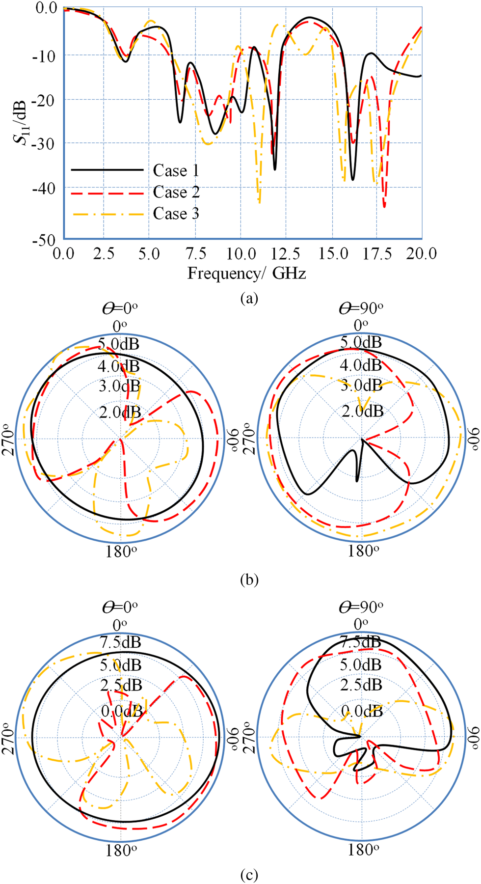
Fig. 3. Antenna performance in terms of S 11 spectra for all cases in (a) and 2-D radiation patterns at 5.8 GHz in (b) and at 8 GHz in (c).
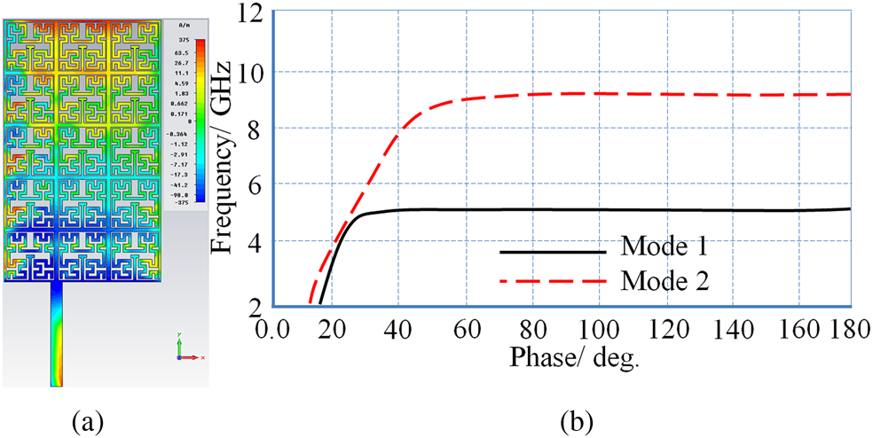
Fig. 4. In (a) current distributions and (b) dispersion diagram.
MTM principles of operation
In this section, the operations of the MTM and the ground plane slots of the proposed work are discussed. As seen in Fig. 3(d), the radiation pattern is significantly affected by the introduction of the MTM structure. In general, the antenna radiation patterns are found to be tangential to the patch surface instead of being broadside radiation patterns as in traditional microstrip antennas [Reference Balanis1]. This can be probably understood from the surface current distribution that is presented in Fig. 4(a), in which the current distribution is mainly concentrated on the patch width (pw) due to the low impedance in comparison to the impedance along the patch length (pl). Hence, the number of unit cells along pw is 3 and along pl is 5. If we treat each unit cell as impedance, this realizes surface impedance along pl higher than the impedance along pw by a ratio of 5/3. For this, the antenna radiation is mainly directed parallel to the patch length. The ground plane defects with the periodical slots are responsible for lowering the antenna quality factor [Reference Palandoken, Grede and Henke16] that increases the bandwidth. As seen in Fig. 4(b), the proposed MTM shows a band gap from 5 to 9 GHz based on the INP substrate as seen in Fig. 4(b).
Bandwidth
To specify the effect of the coupling gap (G) that is shown in Fig. 1(b), S 11 spectra for three different gaps: 0.05, 0.1, and 0.15 mm, are evaluated and presented in Fig. 5. A significant effect of G variation is found on the resonance value, return loss magnitude, and bandwidth. As the G value increases, the bandwidth increases with noticeable degradations in the return loss values. Hence, the G value is considered to be 0.15 mm. An observable effect is found in the antenna matching by changing the length insets of T-shaped stubs inside the Hilbert-shaped unit radiators.
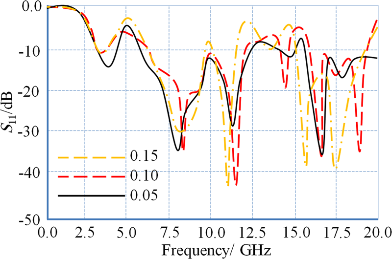
Fig. 5. S 11 spectra change with respect to G variation.
The design of the slotted ground dimensions (Sw) is discussed here. In spite of the major utility of UWB applications, the antenna bandwidth enhancement is analyzed. Figure 6 shows the change in the S 11 spectra with varying slot lines width. This explains the correlative effects of the slot width on the antenna coupling. Moreover, such slots exhibit low spurious feed radiations leakage with matching capacitance at resonating frequencies [Reference Clavijo, Diaz and McKinzie12]. An array of capacitor–inductor (C–L) resonators of parallel branches is modeled to stimulate the effects of the electromagnetic fringing and leakage from the conducted slots [Reference Elwi13]. The values of the C–L branches are relatively affected by the constitutive electromagnetic properties of the substrate ɛr and μr. Moreover, the physical dimensions Sx, ɛr, Sw, and substrate height (h) are directly related to the value of equivalent C–L branches [Reference Elwi13] as:


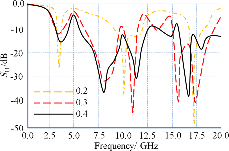
Fig. 6. S 11 spectra change with respect to Sw change.
These equations describe the slots response in terms of bandwidth analytically. Such slots array supports degenerative coupling reduction, which increases the antenna bandwidth significantly as shown in Fig. 6. As explained earlier, the distribution of the current is mainly concentered at the patch width over the patch length to realize a high pl/pw ratio which is relatively proportional to the L/C ratio. In such a case, the introduction of the ground plane defects is justified by increasing the antenna bandwidth through reducing the quality factor [Reference Palandoken, Grede and Henke16]. This also can be explained through two orthogonal field components that are generated along the patch width and length [Reference Sievenpiper, Zhang, Jimenez Broas, Alexopolous and Yablonovitch11] which relatively increases the ratio of pl/pw.
Antenna printing process
The proposed antenna prototypes are manufactured with DMP 2800 material printer as seen in Fig. 7. The nominal drop volume from the printer cartridge is fixed to 10 pl. The cartridge is connected to a piezo-electric head through 16 jets. The INP and FR4 substrates are mounted on the printer heated platen. The platen temperature is raised up to 60°C. To realize a qualified printout, a single ink jet is used with 20 mV pump pressure-driven device. Moreover, the printer head is adjusted to 0.5 mm height from the substrate to avoid ink stream flaring. The same geometry is printed out with five layers and 20 s delay between each consecutive pass to ensure continuous traces. Finally, the annealing process for resulted printouts is conducted at 120°C inside LPKF oven for 10 h. The 50 Ω SMA port is connected to the prototypes using silver paste.

Fig. 7. Fabricated prototypes; (a) and (b) for the FR4 substrate, while (d) and (e) for the INP substrate. The SEM images for the print out on the FR4 and INP substrates are shown in (c) and (f), respectively.
The electrical conductivity of the printout is measured first for FR4 prototype which is found to be 8.8 ± 0.2 × 10⁴ S/m. However, the electrical conductivity is increased up to 9.2 ± 0.2 × 10⁴ S/m when the same structure is printed on the INP substrate. Such conductivity enhancement is attributed to the substrate surface viscosity and smoothness that offer continuous clear printing conductions as can be seen in the SEM images presented in Figs 7(c) and 7(f) for the proposed print out. The top cross-sectional SEM view for the print out on the FR4 substrate shows large crakes that hinder the electron motion in comparison to the print out on the INP substrate. The values of the measured conductivity are used for CST MWS and HFSS simulations.
Antenna performance measurements
Antenna performance under flat conditions
The antenna performance is tested numerically using HFSS software package (www.ansoft.com) based on the finite element method. The fabricated prototypes are measured and compared to each other against numerical simulations as shown in Fig. 8. The simulated S 11 spectra for INP and FR4 prototypes show reasonable agreement with the measurement results as shown in Figs 8(a) and 8(b), respectively. Moreover, the INP prototype bandwidth shows a wider than the one based on FR4 substrate with better matching impedance. The proposed antenna radiation patterns are measured at 5.8 GHz for both prototypes as seen in Figs 8(c) and 8(d) in the E- and H-planes. It is found that the proposed antenna-based INP substrate shows the same gain, about 4.56 dBi, with that of the fabricated-based FR4 substrate. The antenna radiation patterns are measured at 8 GHz as seen in Figs 8(e) and 8(f). It can be revealed that the proposed antenna-based INP substrate shows a gain of 7.38 dBi, while the one based on FR4 substrate is about 6.85 dBi. Such enhancement in the gain is attributed to the radiation focusing when the antenna is mounted on the INP substrate. In general, the measured radiation patterns of both prototypes at 5.8 and 8 GHz are found almost to show identical profiles; thus, changing the substrate type has no impact on the surface current distribution on the antenna patch.
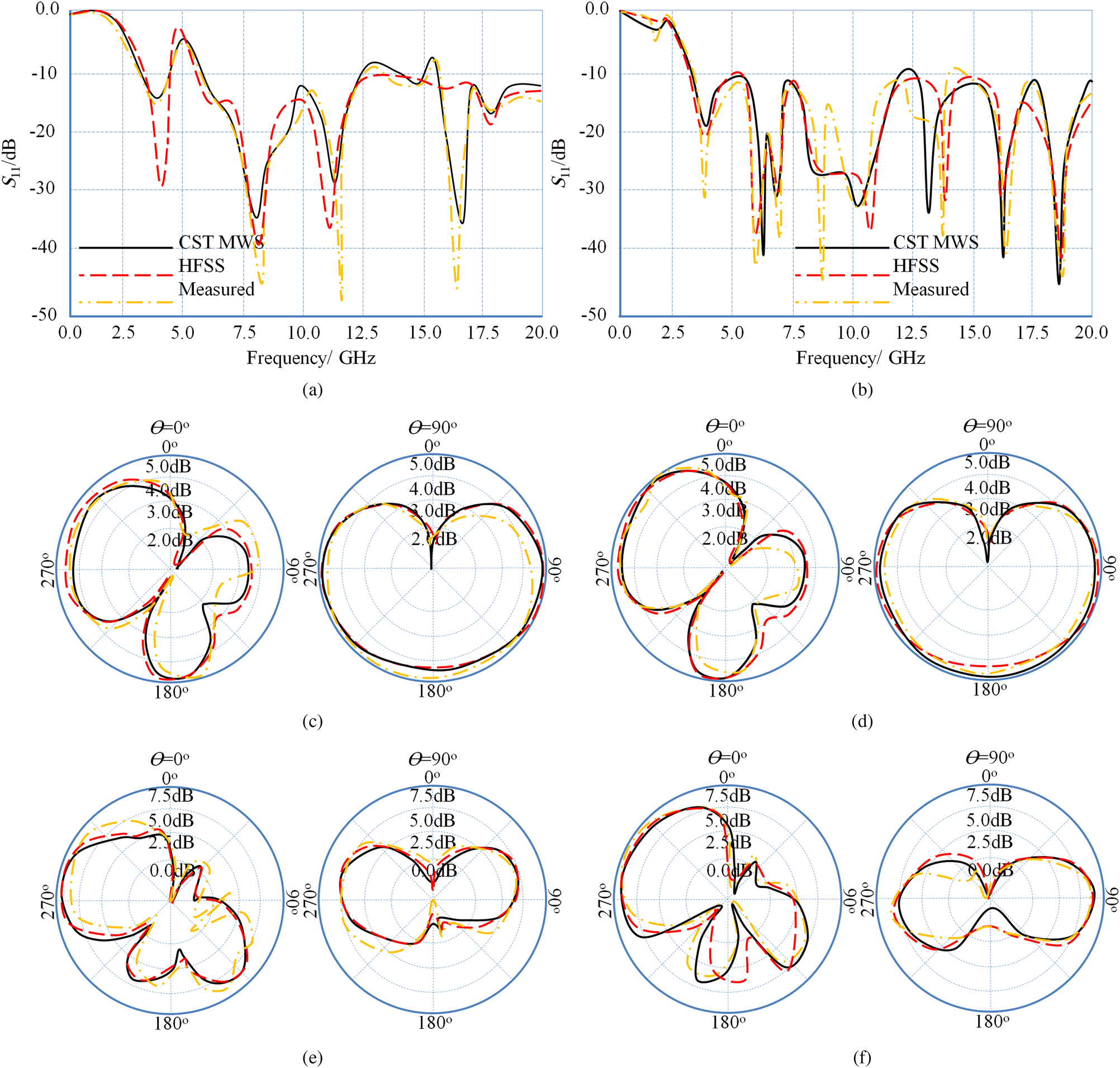
Fig. 8. Measured antenna performance in comparison to the simulated results; (a) S 11 based on FR4 prototype, (b) S 11 based on INP prototype, (c) radiation patterns at 5.8 GHz based on FR4 prototype, (d) radiation patterns at 5.8 GHz based on INP prototype, (e) radiation patterns at 8 GHz based on FR4 prototype, and (f) radiation patterns at 8 GHz based on INP prototype.
Antenna performance under bending conditions
To realize the antenna performance as a flexible structure, the experimental measurements are extended by bending the antennas on two different angles: 10o and 20o. The bended prototypes are measured and compared against their flat profiles as seen in Fig. 9. The measured S 11 spectra for the FR4 prototype show a significant degradation in the matching magnitude as seen in Fig. 9(a). However, for the INP prototype in flat case, the S 11 spectrum is found to be unaffected significantly with bending as depicted in Fig. 9(b). The bended antennas radiation patterns in the E- and H-planes are measured at 5.8 and 8 GHz in comparison to the flat case as seen in Figs 9(c)–9(f). The FR4 prototype gain, at 5.8 GHz, is changed from 4.5 dBi for the flat case to 3.7 dBi than 2.9 dBi, respectively, when it is bended at 10o and 20o as seen in Fig. 9(c). A sever gain degradation is observed in the FR4 prototype, at 8 GHz, from 6.85 dBi for the flat case to 2.1 and 1.5 dBi when it is bended at 10o and 20o, respectively. This is attributed to the side lobes significance after antenna bending. However, the antenna radiation patterns for the INP prototype are mostly unaffected as seen in Figs 9(e) and 9(f). Therefore, the gain of the INP prototype is insignificantly degraded: for example, at 5.8 GHz, the gain for the INP prototype remains almost around 4.5 dBi for both angles of bending. Also, the INP prototype gain at 8 GHz is found to vary from 7.38 dBi for the flat case to 6.5 and 6 dBi when it is bended at 10o and 20o, respectively. This is attributed to the magnetic field storing inside the INP substrate due to the μr component [Reference Elwi and Ahmed5]. Therefore, the radiation patterns of the INP prototype are found almost unaffected with bending.

Fig. 9. Antenna performance with bending effects; (a) and (b) S 11 spectra with FR4 and INP, respectively. (c) and (d) Radiation patterns at 5.8 and 8 GHz, respectively, with FR4. (e) and (f) Radiation patterns at 5.8 and 8 GHz, respectively, with INP.
The performance of the proposed prototypes is compared and summarized in Table 2. From the obtained results, the INP prototype shows excellent immunity against bending effects in comparison to the one based on FR4 substrate that is attributed to μr component of the INP substrate [Reference Ziolkowski and Erentok14]. In another word, the advantage in using INP material is the magnetic field energy can be stored in the INP substrate to help the antenna to radiate regardless the value of the bending angle [Reference Elwi, Jassim and Mohammed20].
Table 2. Antenna performance comparison between the proposed cases

RF energy harvesting
Now, the harvested RF energy at 5.8 and 8 GHz of the proposed antenna-based INP and FR4 substrate prototypes is discussed here. In Fig. 10, the RF harvester of 7 capacitor-based Schottky diodes Villard voltage doubler stages is presented. The chemical etching process is used to manufacture the proposed circuit on Fiberglass Reinforced Epoxy board of 2 mm thickness and ɛr of 3.9. Two SMA ports of 50 Ω input/output matching impedance are connected to the fabricated circuit. The manufactured circuit area is 100 × 40 mm2. A matching load is attached close to the RF input port to maximize the antenna coupling to the RF harvester [Reference Elwi17]. The chock circuit is presented to the RF circuit to reduce the ripple factor in the output DC voltage [Reference Takacs, Aubert, Fredon, Despoisse and Blondeaux18].

Fig. 10. RF energy harvester circuit prototype.
The measured output DC voltage is realized using a UWB stander horn antenna at 5.8 and 8 GHz with a bore-sight gain of 16 and 22 dBi, respectively. The DC voltage is screened on a digital oscilloscope as presented in Fig. 11(a) for both proposed prototypes at 5.8 GHz. It is found that the proposed antenna-based INP substrate shows almost a better enhancement in the output DC voltage from the one based on the FR4 substrate. Nevertheless, the conversion efficiency at 5.8 GHz of the antenna based on the INP substrate is found to be enhanced further more than the one based on the FR4 substrate as depicted in Fig. 11(b). The conversion efficiency is obtained with respect to the power transmitted from the RF source. The same measurements at the output DC voltage and the conversion efficiency are repeated at 8 GHz, to end up with the same previous conclusion. From measurements, the maximum output DC voltage is about 2.98 mV at 5.8 GHz with conversion efficiency of 98% for the INP prototype, while the same prototype is found to provide a maximum output DC voltage of 2.76 mV at 8 GHz with conversion efficiency of 96%.

Fig. 11. RF energy harvesting measurements: (a) output DC voltage at 5.8 GHz, (b) conversion efficiency at 5.8 GHz, (c) output DC voltage at 8 GHz, (b) conversion efficiency at 8 GHz.
In Table 3, a comparison study is provided between the proposed antenna and other published results. Consequently, it can be claimed that the proposed antenna shows superior achievements compared to those published in the literature.
Table 3. Comparison of the proposed antenna validation

Conclusion
In this paper, a miniaturized MTM-based printed antenna circuitry of enhanced gain bandwidth product is presented. The MTM is structured from a Hilbert-shaped unit cell mounted on a flexible INP substrate backed with partial ground plane defected with periodical slots. The same antenna geometry is mounted on the FR4 substrate for comparison. After testing the proposed antennas performance, it is found that the INP antenna shows an enhanced gain bandwidth product in comparison to the identical one based on FR4 substrate. Such enhancement is attributed to the permeability component of the proposed INP substrate. A good agreement is found between the measured and simulated antenna performance for both proposed prototypes. The experimental measurements are extended to evaluate the harvested RF energy based on the collected output DC voltage and conversion efficiency. The effect of bending is studied and it is found that the performance of the prototype-based INP substrate is more immune variation than the one based on FR4 substrate. Finally, it is found that the INP prototype provides an output DC voltage of about 2.98 mV and conversion efficiency of 98% at 5.8 GHz, while the maximum output DC voltage is 2.76 mV with conversion efficiency of 96% at 8 GHz.
 Taha A. Elwi received his B.Sc. degree in the electrical engineering department (2003) (Highest Graduation Award), Postgraduate M.Sc. degree in laser and optoelectronics engineering department (2005) (Highest Graduation Award) from Nahrain University Baghdad, Iraq. From April 2005 to August 2007, he was working with Huawei Technologies Company, Baghdad, Iraq. On January 2008, he joined the University of Arkansas at Little Rock and he obtained his Ph.D. degree in December 2011 from the system engineering and science department. His research areas include wearable and implantable antennas for biomedical wireless systems, smart antennas, Wi-Fi deployment, electromagnetic wave scattering by complex objects, design, modeling and testing of metamaterial structures for microwave applications, design, and analysis of microstrip antennas for mobile radio systems, precipitation effects on terrestrial and satellite frequency re-use communication systems, effects of the complex media on electromagnetic propagation and GPS. The nano-scale structures in the entire electromagnetic spectrum are a part of his research interest.
 Ali M. Al-Saegh received his B.Sc. degree in electronic and communications (2005), and M.Sc. degree in satellite engineering (2008) from electronic and communications engineering department in Nahrain University, Baghdad, Iraq. He received his Ph.D. degree in wireless communications engineering from computer and communication system engineering department in Universiti Putra Malaysia (UPM), Selangor, Malaysia, in 2015. From 2009 to 2012, he was attached as a lecturer in computer engineering techniques and communications engineering departments in Al-Ma′moon university college, Iraq. From 2012 to 2013, he was a research assistant in the department of computer and communication systems engineering, UPM, Malaysia. Since 2015, he has been a senior lecturer in computer engineering techniques department in Al-Ma'moon university college, Iraq. His areas of specialization are radio waves propagation, satellite communications, atmospheric impairments prediction, channel modeling, mitigation techniques, multimedia transmission, and resource management.


