INTRODUCTION
Pulsed power systems are very important tools to produce high power beams, which are used in high energy density physics, and inertial fusion (Chuvatin et al., Reference Chuvatin, Kokshenev, Aranchuk, Huet, Kurmaev and Fursov2006; Liu et al., Reference Liu, Li, Zhang, Li and Wang2006, Reference Liu, Yin, Ge, Zhan, Chen, Feng, Shu, Zhang and Wang2007a, Reference Liu, Zhan, Zhang, Liu, Feng, Shu, Zhang and Wang2007b; Tarasenko et al., Reference Tarasenko, Shunailov, Shpak and Kostyrya2005; Wang et al., Reference Wang, Hu and Song2005; Winterberg, Reference Winterberg2006; Yatsui et al., Reference Yatsui, Shimiya, Masugata, Shigeta and Shibata2005; Zou et al., Reference Zou, Liu, Zeng, Han, Yuan, Wang and Zhang2006). A pulsed power diode used to produce high power particle beam is driven by a pulsed generator that often consist of a Marx generator, a pulsed forming line (PFL), a main switch, and a pulsed transmission line (PTL). In the diode there is usually an unwanted prepulse appearing prior to the main pulse. This prepulse is a result of the main switch coupling PFL voltage to PTL during the time of PFL being charged by Marx generator. The prepulse is harmful to the optimum operation of the diode. Therefore, reducing the prepulse is important, especially for an electron beam diode with low impedance and high current (Parker et al., Reference Parker, Anderson and Duncan1974). For a graphite cathode and a prepulse of 1µs in pulse width, it is required that the electrical filed in the gap between the anode and the cathode (A-K gap) is less than 12 kV/cm (Qiu et al., Reference Qiu, Zhang, Luo, Zheng, Peng, Gai, Huang, Tang, Ren, Shao, Chen, Li and Yang2003). High energy fluence electron beam could be obtained by decreasing emission area of the cathode and increasing the magnetic mirror ratio (Liu et al., Reference Liu, Qiu and Zhang1994). Since A-K gap of a diode is decreased in proportion to the cathode diameter, a prepulse of lower amplitude would be more desirable. For this purpose, a flash-over switch was usually inserted on the cathode stalk just upstream of the diode to eliminate the prepulse (Menge et al., Reference Menge, Maenchen, Mazarakis and Rosenthal1999; Allen et al., Reference Allen, Boller, Commisso and Young2001). As the flash-over length and the flash-over voltage of the flash-over switch increase, however, more energy from the main pulse would be lost due to the flash-over and damage to the surface of the diaphragm that isolates the cathode from the anode would result due to being exposed to the Ultraviolet (UV) emission emitted from the flash-over. In this article, we report the efforts made to increase length of flash-over switch for reducing prepulse on condition without increasing the flash-over voltage of the switch.
EXPERIMENTAL FACILITY AND FLASH-OVER SWITCH
High energy fluence diode was powered by an accelerator, FLASH-II. Figure 1 shows the block diagram of FLASH-II that consists of a 6 MV Marx generator, a 5-Ohm and 80-ns PFL, a main switch, a 3.2-Ohm PTL, a prepulse switch, a 2-Ohm pulse output line (POL), and a 2-Ohm diode with a flash-over switch.

Fig. 1. Block diagram of FLASH-II accelerator.
A long rod insulator inserted between the cathode stalk and the cathode is called a flash-over switch, which is equivalent to a capacitor connected in series with the capacitor of A-K gap during the period of prepulse. The voltage of the prepulse is divided by the flash-over switch and diode, leading to a lowering of the prepulse applied to the A-K gap. Primary electrons emitted from the triple junction of the cathode stalk move toward the cathode during the front edge of the main pulse. Almost all of these electrons are turn by self-magnetic field force and bombard the surface of the insulator, and causes a secondary emission on the surface. This process, as shown in Figure 2, will last until the electrons arrive to the cathode in “jump mode” and flash-over happens along the surface of the insulator. In this way, the main pulse is delivered to the A-K gap along the surface of the insulator.

Fig. 2. Surface breakdown process of insulator.
In vacuum, the breakdown field of the insulator surface by a pulse of an effective pulse width from 30 ns to 1000 ns can be calculated with the following formula proposed by Martin et al. (Reference Martin, Guenther and Kristiansen1996).
where E is the electric field in unit of kV/cm, t eff is the effective pulse width in unit of µs, i.e., the time duration of the pulse exceeding 89% peak value; A is the area of insulator surface in unit of cm2; K is a constant depending on the pulse width and about 170 averaged over the experimental results (Watson, Reference Watson1967; Milton, Reference Milton1972) for the pulse width in range of 0.03–0.5 µs.
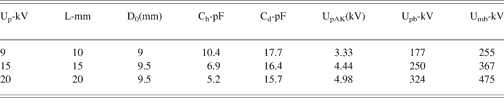
Using Eq. (1) the flash-over voltages along the surface of a solid insulator, 120 mm in diameter, used as our flash-over switch were calculated. In the calculation, t eff was taken to be 100 ns for the prepulse and 10 ns for the main pulse. The results of calculation are shown in Table 1. In Table 1, U p and U pAK are the total prepulse voltage and the prepulse applied to A-K gap, respectively; L and d o are the length of the solid insulator and the length of the A-K gap, respectively, C h and C d are the equivalent capacitance of the flash-over switch and that of the A-K gap, respectively; U pb and U mb are the breakdown voltage for the prepulse and for the main pulse during its front edge, respectively.
Table 1. The calculated results of the flash-over switch

As can be seen from Table 1 that although the amplitude of the prepulse is proportional to the primary charge voltage of accelerator, the prepulse applied to the K-A gap of the diode could be kept below 5 kV by using a flash-over switch of different length L. But it should be noticed that if a flash-over switch with an insulator length of 20 mm is used, the breakdown voltage during front edge of main pulse would be as high as 475 kV at which energy from the main pulse would be lost.
EXPERIMENTS AND DISCUSSIONS
There are many factors such as the angle between the surface of electrode and the insulator, the quality of the insulator, the surface treatment, and the waveform of the applying voltage that affect the flash-over voltage of a flash-over switch. From the experiment done by Milton (Reference Milton1972) cylinder is the best structure for decreasing the flash-over voltage of the flash-over switch. Two kinds of flash-over switches made of Nylon cylinder and ABS cylinder have been studied in our experiments. By comparing the diode voltage and the diode current of the nylon cylinder with those of the ABS cylinder, it was found that the waveforms with nylon appear 2–3 ns earlier than those with acrylonitrile butadiele styrene (ABS), which means the flash-over voltage of ABS switch is higher than that of Nylon switch.
When the diode voltage was 1.23 MV and a flash-over switch made of a 10 mm long insulator was used, the prepulse could be decreased from 9 kV to 3.3 kV and the flash-over switch broke down at 255 kV at the front edge of the main pulse. The output of the diode was reproducible and no obviously negative effects on the main pulse were found from the introducing this flash-over switch.
As the diode voltage was raised up to 1.35 MV, the insulator length of the flash-over switch was increased to 15 mm. Although the prepulse could be lowered from 15 kV to 4.4 kV, this flash-over switch was proved to be not good enough for the diode to work well. Breakdown of A-K gap or flash-over along the surface of the diaphragm that isolates the cathode from the anode sometimes happens during the period of the main pulse. The breakdown of A-K gap could be attributed to the high diode current of 500 kA as well as the corresponding high current density of 4.4 kA/cm2. Under this condition, the cathode plasma is so intense that it induces the breakdown of the A-K gap. As for the flash-over of the diaphragm surface, it may result from the flash-over of the switch happening at a too high voltage that produces strong UV photons bombing the diaphragm surface. All of these indicate that both the prepulse voltage of the A-K gap and the flash-over voltage of the switch should be further reduced.
The above experimental results show that a stable operation of the diode could hardly be achieved only by adjusting the parameters of the flash-over switch, thus, we also tested other techniques among which is the so-called “secondary prepulse technique” (SPT). If the prepulse switch shown in Figure 1 breaks down at the same time or a little bit earlier than the main switch, the prepulse on the PTL would transfer to the POL and diode, forming a SPT, a pulse with a pulse width of about 40 ns, which is much shorter than the first prepulse with a pulse width of about 700 ns, and an amplitude of about 250 kV. Figure 3 shows the secondary prepulse, relatively smaller in amplitude, appearing ahead of the main pulse.

Fig. 3. Waveform of the diode voltage with the secondary prepulse.
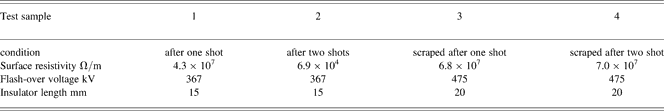
We compared the flash-over delays of the flash-over switch in case of using SPT and without using SPT. It was found that the averaged delay of the 20-mm flash-over switch using SPT is 20.2 ns, 2 ns shorter than that of the 15-mm flash-over switch without using SPT. In this way we obtained, respectively, a lower prepulse voltage of A-K gap by using a longer flash-over switch and a lower flash-over voltage of the flash-over switch by using SPT. SEM images of the switch insulator surface after 1–2 shots are shown in Figure 4. While some flexural and shallow discharge channels of about 4 µm in width were left on the insulator surface after one shot (Fig. 4a), a straight and deeper channel of about 6 µm in width was observed on the insulator surface after two shots (Fig. 4b). Figure 4c shows the insulator surface scraped 0.5 mm thick material away to remove the discharge channel left by one shot. The flash-over considerably changes not only the surface topography of the switch insulator but also its surface resistivity. Table 2 list the results of the resistivity measurements. The surface resistivity of the flash-over switch made from Nylon was decreased from 2.0 × 10⁹ Ω/m before using to 4.3 × 10⁷ Ω/m after one shot. If one more shot was made, the surface resistivity would further decreased to 6.9 × 10⁴ Ω/m. It is important to understand that the flash-over voltage of the switch strongly depends on the surface resistivity and a surface resistivity on the order of 107 Ω/m is most suitable for the 20-mm flash-over switch to operate stably at a lower flash-over voltage. This optimal value is achieved after one shot or by scraping 0.5 mm thick material away from the surface after two shot for 20 mm flash-over switch.

Fig. 4. SEM images of the switch insulator surface after 1–2 shots.
Table 2. Surface resistivity of Nylon flash-over switch after 1–3 shots
CONCLUSION
The prepulse of diode was effectively lowered by inserting a flash-over switch between the cathode stalk and the cathode. A longer insulator is usually used as the flash-over switch when the charge voltage of pulse forming line is higher. In this case, secondary prepulse technique could be used to decrease the flash-over voltage of the switch. In addition to the secondary prepulse technique, making the switch insulator have an optimal surface resistivity could also decrease the flash-over voltage. It was found that a surface resistivity on the order of 107 Ω/m is most suitable for the flash-over switch made of 20-mm nylon insulator to operate stably at a lower flash-over voltage. This optimal value is achieved after one shot for 15 mm flash-over switch or by scraping 0.5 mm thick material away from the surface after each shot for 20 mm flash-over switch.