


Introduction
High power microwave (HPM) systems are an integral part of the modern electromagnetic (EM) warfare [Reference Benford, Swegle and Schamiloglu1]. The development of HPM systems is also being done for testing how much safe our defense or civilian electronic equipments are, for any possible electromagnetic attack. The effect of EM attack is similar to the electrical disturbance/blackout during a nuclear explosion. The nuclear explosion also generates a high-power EM pulse. Such EM pulse, if generated intentionally in a controlled environment, can disturb or destroy electronics without any harm to living beings in an inhabited area and gives an edge over the enemy in a war situation. The “soft-kill” requires lesser power (of the order of Megawatts, since it causes only disturbance in electronics) than “hard-kill” which may permanently breakdown or physically damage the electronic system [Reference Guoqi and Junwei2]. In some space applications and Radars, the microwave power in kilo-Watts to few mega-Watts range is used for large distance communication and surveillance.
Microwave sources, such as Vircator (Virtual Cathode Oscillator), Magnetron, Gyrotron, MILO (magnetically insulated line oscillator), BWO (backward wave oscillator) etc. generate output power in the form of higher-order modes (of the circular waveguide) [Reference Benford, Swegle and Schamiloglu1]. Due to the circular symmetry of these sources, the output power is emitted in the form of TEM or TM 0n modes. Due to the lowest cutoff frequency, TM 01 mode contains most of the power. Also, TEM mode can be easily converted to TM 01 mode through proper matching between coaxial and hollow waveguide. For radiation through a conical horn antenna, TE 11 mode is the useful mode. Therefore, a mode converter to convert higher mode (TM 01) to TE 11 mode is required between the microwave source and horn antenna.
Conventional mode converter designs consist of a hollow circular waveguide with dual bends or serpentine shape [Reference Lawson, Arjona, Hogan and Ives3–Reference Yuan, Huan and Liang9]. These designs exhibit high conversion efficiency but have a disadvantage of non-aligned ports and nonlinear waveguide axis, which makes the structure non-compact. Other types of mode-converter designs consist of linear axis circular waveguides [Reference Tribak, Zbitou, Mediavilla and Touhami10–Reference Chittora, Singh, Sharma and Mukherjee21], in which both of the ports are aligned. These designs have some perturbation in the waveguide to perform mode conversion operation. The perturbation in waveguide limits the conversion efficiency as well as power handling capability. Some of the designs [Reference Wang, Qin, Xu and Shi16, Reference Chittora, Singh, Sharma and Mukherjee19–Reference Chittora, Singh, Sharma and Mukherjee21] are based on the principle of phase shift in the lower semicircular waveguide. The phase shift can be provided by the perturbation caused due to pure dielectric [Reference Chittora, Singh, Sharma and Mukherjee19, Reference Chittora, Singh, Sharma and Mukherjee20] or pure metallic [Reference Chittora, Singh, Sharma and Mukherjee21] structures. The perturbing structure also adds extra weight to the converter. The perturbing structure has to be appropriately chosen or designed so that the reflection of input TM 01 mode remains minimum towards the source, and conversion efficiency to TE 11 mode is maximized.
Printed substrate-based designs have not been considered yet for mode conversion. Such designs can prove to be very lightweight and low cost for portable and airborne microwave systems. Periodic loading of the printed substrate in the waveguide is reported in the literature for designing EBG structure, slow-wave structure (SWS), metamaterial structures, and also for slow-wave effect in rectangular waveguides [Reference Kshetrimayum and Zhu22, Reference Kshetrimayum and Zhu23].
This paper presents the effect of periodic loading of printed substrates in a circular waveguide to provide a relative phase shift for mode conversion. An earlier version of this paper was presented at the IMaRC-2018 Conference and was published in its Proceedings [Reference Chittora24]. Each printed substrate is equivalent to reactive loading in equivalent transmission line and can provide some phase shift to the propagating fields, based on the design. The total phase shift of 180° can be achieved by repetitive (periodic) loading of the same printed substrate.
Design principle
Among all TM 0n modes generated by microwave source (e.g. Vircator, Magnetron, BWO, MILO), TM 01 mode has the lowest cutoff frequency and therefore most of the power propagates in the form of TM 01 mode. The output port of these sources is generally large in size to handle high power levels. Large output diameter can result in higher-order mode generation along with TM 01 mode and fundamental TE 11 mode. TE 11 mode is the most favored mode in a circular waveguide and can be present along with TM 01 mode in waveguide. Since most of the power is in TM 01 mode, it is desirable to get pure TM 01 mode output from the source. Also, at the operating frequency, the converter diameter is smaller than the source diameter to avoid higher-order mode propagation. Therefore, a transition waveguide is connected between the HPM source and mode converter, which transmits only TM 01 and TE 11 modes at high efficiency and also matches the diameter of the source and mode converter [Reference Chittora, Singh, Roy, Sharma and Mukherjee25].
In this paper, the mode converter is designed at 3.2 GHz operating frequency. The diameter of the mode converter waveguide is taken as 9 cm so that the operating frequency 3.2 GHz is sufficiently larger than the cutoff frequency of TM 01 and TE 11 modes. The proposed mode converter design consists of a circular waveguide (CWG) partitioned using a horizontal metallic plate. It results in two semicircular waveguide (SWG) sections, one of which is hollow and other is loaded. The lower SWG is loaded with periodic and parallel semi-annular substrates (with inner radius rin) as shown in Figs 1 and 2. Each substrate consists of metallic strips on one side and the copper is completely removed from the other side. The strips on the substrate are radially diverging towards the waveguide wall (to support the electric field of input SWG TE11 mode) and do not connect to the waveguide wall. The strips face the input (port) side of the mode converter.
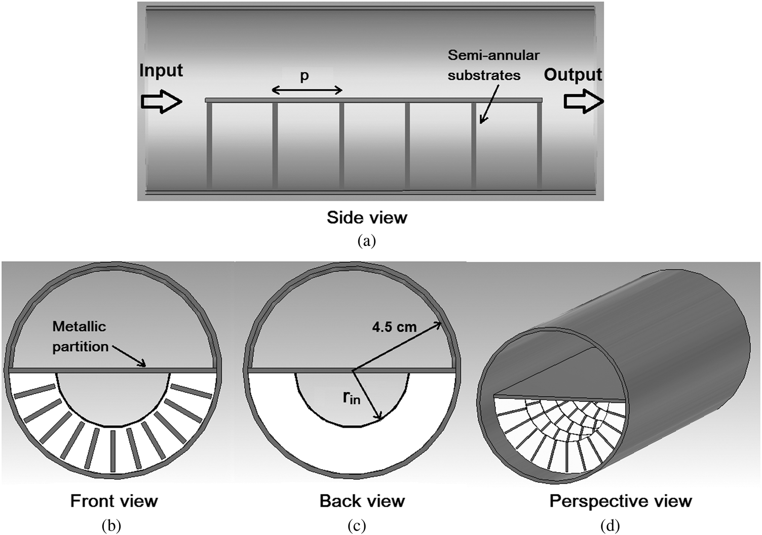
Fig. 1. Design of the proposed TM 01 to TE 11 mode converter with different views. (a) Side view, (b) front view, (c) back view, (d) perspective view.
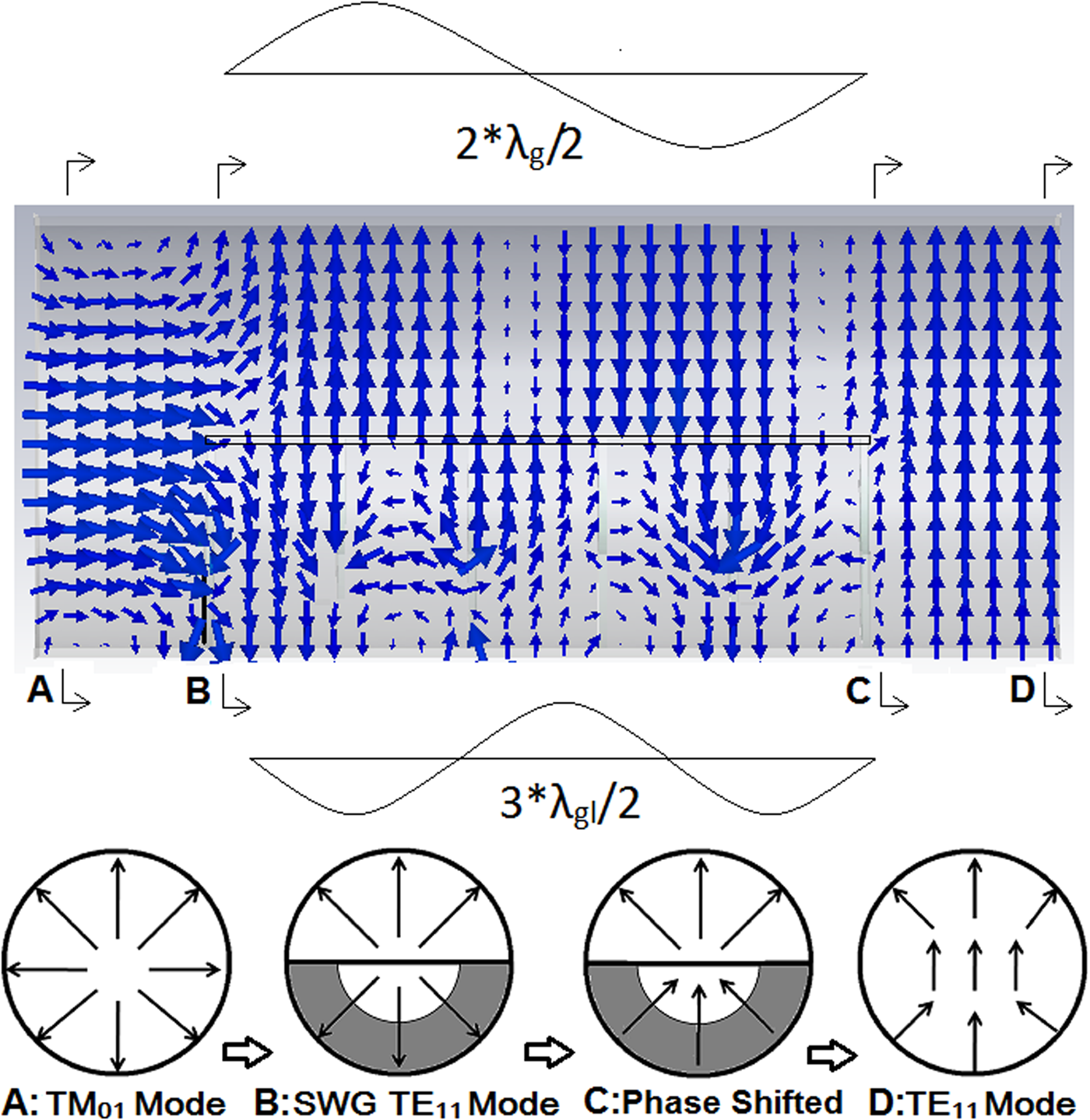
Fig. 2. Process of TM 01-TE 11 mode conversion along the length of the converter at different cross sections. A: TM 01 mode, B: SWG TE 11 mode, C: phase shifted, D: TE 11 mode.
Substrates are placed parallel and periodically in lower SWG at a certain gap/distance (p) from each other. Effectively, the periodic structure works as an artificial dielectric medium and provides the required total phase shift of 180° in lower SWG. When TM 01 mode is given as input it is divided into two SWG TE 11 modes at the metallic partition. Since the upper SWG is hollow, the fields propagate without delay. But in lower SWG, due to periodic loading, a phase shift is introduced to the propagating fields. For mode conversion, total 180° phase shift is required between upper and lower SWG fields.

where βg and βgl is propagation constant in hollow and substrate loaded SWGs respectively, and L is the total length of the converter section. In loaded waveguide, the electric field lines of the SWG TE 11 mode are terminated due to metallic strips, at a slightly smaller distance before the usual termination and causes a decrease in guided wavelength (λgl < λg). It results into partial path (or phase) difference. The partial phase difference at each substrate sums up to 180° phase difference (equivalent to half guide wavelength) at the end of Nth substrate. If upper SWG supports λg, then to provide a relative phase shift of 180° between upper and lower SWGs, the lower SWG should support 3λgl/2 of fields (or βgl = 3βg/2). The process of mode conversion is shown in Fig. 2. If lower SWG is loaded with N-substrates, each with a gap p, then using equation (1),

or

The initial value of gap (p) between substrates can be calculated using equation (3). It can be further optimized using electromagnetic solver. The E-field lines of SWG TE 11 mode in lower SWG, meet completely in-phase with respect to the upper SWG TE 11 mode at the end of Nth substrate. At the end of the metallic partition, both SWGs are joined together to make a hollow CWG and the in-phase SWG TE 11 modes combination results into CWG TE 11 mode.
Efforts have been made to minimize the size of the proposed design by reducing the number of substrates and the gap between substrates. The parametric analysis to achieve the most compact design with high conversion efficiency is discussed in the next section.
Results and discussion
The proposed mode converter is designed and simulated in electromagnetic solver CST Microwave Studio®. As discussed in the previous section, there are the following design parameters, which affect the mode conversion efficiency:
(1) Dielectric constant (ɛr) and thickness (h) of the substrate.
(2) Shape and dimension of the substrate.
(3) Number (n) and orientation of strips on the substrate.
(4) Periodicity: total number of substrates (N) and gap between two substrates (p).
Due to cost-effectiveness FR4 is used as dielectric substrate with dielectric constant ɛr = 4.4, loss tangent = 0.025, and thickness h = 1.6 mm. Other dielectric substrates can also be used to reduce losses and to improve power handling capability. Parametric analysis is performed with respect to important design parameters to achieve the optimum values for high mode conversion efficiency, compact shape, and size at the operating frequency.
Shape and dimension of the substrate
Each FR4 substrate is cut in a semi-annular shape with inner radius rin and outer radius as 4.5 cm, which is equal to the waveguide radius. The front side (input side) of each substrate consists of radially diverging metallic strips. In Fig. 3, the effect of the varying inner radius (rin) of semi-annular substrate from 2.4 cm to 2.7 cm is illustrated, keeping all other parameters constant. It is evident that maximum efficiency at 3.2 GHz is achieved with rin = 2.6 cm. The cutoff frequency of different modes is shown in Table 1 for the 9 cm diameter circular waveguide.

Fig. 3. Mode conversion efficiency with respect to inner radius (rin) of the semi-annular substrates.
Table 1. Cutoff frequency of different circular waveguide modes for radius = 4.5 cm

Number (n) and orientation of metallic strips on the substrate
Since TM 01 mode consists of electric field lines in the radial direction, metallic strips are printed symmetrically on FR4 substrate to execute the phase delay operation in lower SWG. Width of each strip is taken as 1 mm to keep the reflection minimum. The number of strips on the substrate is varied as n = 9, 11, and 13 (angular gap of 18°, 15°, and 12.86° respectively) and optimized for high mode conversion efficiency as shown in Fig. 4.

Fig. 4. Mode conversion efficiency with respect to number of strips (n) on each semi-annular substrate.
Although the results are very close to each other, a higher number can cause more reflection to the input mode. Maximum conversion efficiency and bandwidth is achieved with 11 metallic strips (15° angular gap) on each substrate. Each metal strip extends in radial direction from 2.6 to 4.4 cm on the substrate from center of the waveguide cross section, i.e. the metal strips are electrically disconnected from the waveguide wall. The back side of the substrate is completely etched.
Periodicity: total number of substrates (N) and gap (p) between two substrates
It is important to investigate the role of periodicity on mode conversion efficiency. The number of semi-annular substrates is taken as six and other parameters are kept constant. Figure 5 illustrates the effect of gap (p) between substrates on mode conversion efficiency. The gap between substrates is varied from 2.6 to 3.2 cm keeping other design parameters constant and corresponding conversion efficiency is plotted. The maximum efficiency is achieved at a gap p = 2.8 cm between the substrates, which is very close to the theoretical value (2.4 cm) calculated using equation (3).

Fig. 5. Mode conversion efficiency with respect to gap (p) between the substrates.
The optimized values of the design parameters are summarized in Table 2. The converter is simulated using the optimized parameter values. The maximum efficiency of 99.2% is achieved at 3.2 GHz with six semi-annular substrates placed at a distance (gap) of p = 2.8 cm consecutively in lower SWG. Mode conversion efficiency is more than 90% over a bandwidth of 180 MHz (relative bandwidth 5.6% at the operating frequency) as shown in Fig. 6. Reflection and transmission of TM 01 mode and conversion to higher (TE 21) mode also remain below 5% in the converter bandwidth. If TE 11 mode is present at the input port, it will be reflected back towards the source. Therefore, it is important that the input power should be in the form of pure TM 01 mode. TE 21 mode at input port can be suppressed by taking the appropriate waveguide diameter, such that TE 21 mode cutoff frequency becomes greater than operating frequency or mode conversion bandwidth.

Fig. 6. S-parameter plot of the proposed mode converter for pure TM 01 mode at the input port.
Table 2. Optimized values of design parameters for the proposed mode converter

The proposed mode converter is fabricated as shown in Fig. 7. To excite the TM 01 mode at input port a biconical shape feed [Reference Chittora, Singh, Sharma and Mukherjee27] is designed and applied at the input port axis of the mode converter. The TM 01 mode feed has high efficiency in 3–4 GHz range and suitable for low power measurements of the mode converter. The reflection coefficient of TM 01 mode at the input port is measured using Vector Network Analyzer (VNA) and compared with the simulated result as shown in Fig. 8. The reflection coefficient is well below −10 dB in the mode converter bandwidth and agrees with the simulation result. The radiation pattern is also measured in the anechoic chamber to verify the mode conversion and results are shown in Fig. 9. The pattern is first measured without mode converter and the minimum is observed at the center of radiation patternplot. In the next step, the measurement is performed with the mode converter. It is evident from Fig. 9 that the radiation pattern has a maximum at the center and is similar to the pattern obtained with TE 11 mode. This verifies the desired TM 01–TE 11 mode conversion with radiation pattern method.

Fig. 7. Fabricated mode converter waveguide and radiation pattern measurement setup in the anechoic chamber.

Fig. 8. Simulated and measured reflection coefficient of TM 01 mode input to the mode converter.

Fig. 9. (a) and (b) measurement setup and (c) radiation pattern, without (dotted curve) and with mode converter (solid and dash curve) at 3.2 GHz.
Mode conversion efficiency is also measured using the setup as shown in Fig. 10. TM 01 mode feed and TE 11 mode detector are applied at the input and output port of the mode converter respectively. The measured mode conversion efficiency is plotted as shown in Fig. 11 with simulated efficiency. The measured efficiency plot follows the simulated efficiency and has dips due to multiple reflections in a close waveguide structure. The figure also includes simulated efficiency plots, “without dielectric” and “without metallic strips” loading (dashed and dotted curve, respectively). It confirms that the mode conversion phenomenon is due to the combined effect of dielectric and metallic strip structure of the loaded periodic substrates.

Fig. 10. Measurement setup for the TM 01–TE 11 mode conversion efficiency.

Fig. 11. Simulated and measured results for TM 01–TE 11 mode conversion efficiency.
The power handling capability of the converter is estimated by maximum electric field appearing in the mode converter using simulation. The maximum electric field remains below 200 kV/cm (limit for dielectric) for 10 MW input signal, therefore the estimated power handling capability of the converter is up to 10 MW. A comparison of the mode converter designs is presented in Table 3 with the proposed design. The proposed design is very compact with respect to diameter and length compared to other designs (except [Reference Yuan, Zhong, Liu and Qian12], for which the bandwidth data are not available). Since only a thin metallic partition and dielectric substrates are used in the structure, it presents a very lightweight, compact and low-cost solution to the mode converter design.
Table 3. Comparison of the proposed and previously reported mode converter designs in the literature.

M, metallic; D, dielectric; NP, not provided.
Conclusion
In this paper, a printed substrate loaded TM 01–TE 11 mode converter design is presented. The substrates are placed periodically in a lower semicircular waveguide section to provide the required phase shift for mode conversion. The maximum conversion efficiency of 99.2% is achieved at an operating frequency of 3.2 GHz. Relative bandwidth of 5.6% (180 MHz) is also observed at the operating frequency. Power handling capability is limited to 10 MW due to dielectric based design. It can be improved by using an appropriate medium (e.g. SF 6) and high dielectric strength substrate material up to three times. The proposed structure is a compact, lightweight, and low-cost solution for mode conversion. It is easy to fabricate and install on portable and airborne HPM systems.
Acknowledgement
The author would like to thank Prof. K. R. Anupama for providing the antenna measurement facility.
 Ashish Chittora received the B.E. degree in electronics and communication engineering from Engineering College, Kota, India, in 2009, M.E. in electronics and communication engineering from Delhi College of Engineering, Delhi, India, and Ph.D. In Electrical Engineering from IIT Bombay, Mumbai, India in 2016. He worked at Amity University, Noida, India as an assistant professor and currently he is Assistant Professor in Electrical and Electronics Engineering Department at BITS Pilani, K K Birla Goa Campus. His research interests include high power microwave passive devices and antennas.
 Swati Varun Yadav received her B.E. degree in Electronics and Communication Engineering from M.I.T, Ujjain (India) in 2007 and received his M.E. degree in Digital Communication from Rajiv Gandhi Proudyogiki Vishwavidyalaya, Bhopal (India) in 2011. She has been pursuing her Ph.D. degree from Department of Electrical & Electronics Engineering, Goa Campus, BITS, Pilani (India) since 2019. Her fields of interest are high-power microwave passive devices.


