Introduction
Dielectric resonator (DR) has been widely applied in modern wireless communication systems, principally owing to its high unloaded quality factor (Q u), small size, and superior temperature stability. The DR is generally loaded in a metal cavity (made from aluminum or copper material generally) for designing high-performance filters with single-ended, balanced or balun topologies [Reference Kishor, Kanaujia, Dwari and Kumar1, Reference Chen, Li, Zhan, Qin, Shi and Bao2] for meeting various practical requirements. To miniaturize the filter size, dual-/triple-mode DRs [Reference Pelliccia, Cacciamani, Tomassoni and Sorrentino3–Reference Wong, Zhang, Feng, Chen, Xue and Zhu5] are extensively explored because they can be used as a doubly/triply tuned resonant circuit. However, in the designs of the DR filters, the metal cavity is usually indispensable, which would result in three-dimensional (3-D) bulky structure, heavy weight, and high cost.
Comparatively, planar transmission line (e.g. microstrip and strip line) resonators and filters are with simple structure, light weight, and easy integration with other microwave components/devices. However, they possess a relatively low Q u, and then high in-band loss. This problematic issue will become worse as the operation frequency increases due to the decrease of the skin depth in the metal line [Reference Du, Ma and Mou6, Reference Du, Ma and Mou7]. In the past few years, substrate integrated waveguide (SIW) [Reference Azad, Jhariya and Mohan8, Reference Cheng, Lin, Lancaster, Song and Fan9] resonators have been developed to improve Q u, but the improvement is limited due to the surface currents existing on the top and bottom metal layers. The new methodology [Reference Parment, Ghiotto, Vuong, Duchamp and Wu10, Reference Belenguer, Esteban and Boria11] for manufacturing empty waveguides in a planar substrate is proposed. In [Reference Belenguer, Esteban and Boria11], devices manufactured with this empty substrate integrated waveguide (ESIW) technique present lower losses and higher quality factor over the equivalent design using the traditional SIWs. However, the ESIW structure shows a relatively large size. Recently, the authors' group has proposed a dielectric-strip resonator [Reference Zhu, Li and Chen12] and a new low-profile dual-mode dielectric patch resonator [Reference Chen, Li, Yang and Bao13], however, the assembly of these filters is troubling, e.g. alignment of the employed resonators during the process of gluing them with the bottom substrate. Moreover, extra metal cavity in the two designs is required for shielding.
In this paper, a novel dual-mode DR is constructed for the first time by using the multilayer printed circuit board (PCB) technology, and it is made of the high permittivity substrate. Meanwhile, the proposed resonator self-packaged in an equivalent cavity implemented by multilayer PCBs is theoretically investigated, and a pair of degenerate TM11 modes (dominate mode) are used for designing bandpass filter, featuring low in-band loss, compact size, and light weight.
Proposed PCB-based DR
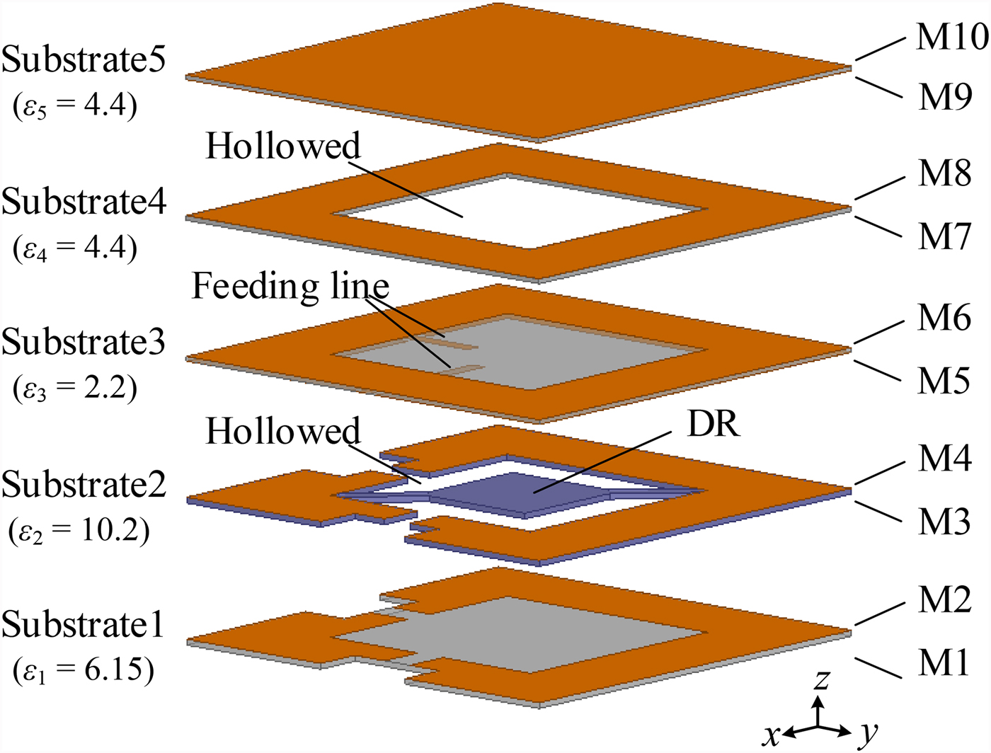
Figure 1 shows the 3-D view of the proposed dual-mode PCB-based DR filter which consists of five individual layers of substrates named Substrate1-5, and 10 metal layers, i.e. M1–M10, on both sides of each substrate. These five substrates are chosen as follows. Substrate1 is 0.635-mm-thick Rogers RO3006 (ε 1 = 6.15 and tanδ = 0.0025). Substrate2 is 0.635-mm-thick Rogers RO3010 (ε 2 = 10.2 and tanδ = 0.0035), which is etched to shape the DR. Substrate3 is 0.508-mm-thick Rogers RO5880 (ε 3 = 2.2 and tanδ = 0.0009) where there is a pair of feeding lines at the bottom of this substrate. Substrate4 and Substrate5 are 0.5-mm-thick FR4_epoxy (ε 4, ε 5 = 4.4 and tanδ = 0.015).

Fig. 1. 3-D view of the proposed dual-mode PCB-based DR filter.
Figure 2 shows the brief sketch of the proposed PCB-based DR with the volume of a × b × L for analysis, where the substrate with a relative dielectric constant ε 1 and a thickness of h 2 at the bottom of the metal cavity supports the DR with a relative dielectric constant ε 2 and a thickness of L, while ε a = 1 represents the air here. In this analysis model in Fig. 2, the substrate and DR are considered as the pure dielectric, where there exist no surface electric current density (J s) on the interface [Reference Balanis14] between the substrate and DR. According to the electromagnetic field boundary conditions, the E-field and H-field are continuous in the tangential direction on the interface between them. Hence
 $$\left\{ \matrix{e_n \times (H_1-H_2) = 0 \hfill \cr e_n \times (E_1-E_2) = 0 \hfill} \right.,$$
where e n denotes the normal to the interface between the two-layer of dielectrics. E 1, E 2 and H 1, H 2 denote the E-fields and the H-fields of the substrate and DR, respectively. The effect of the top and bottom metal walls is to modify the exponential decay of the field components into a hyperbolic z dependence. In the DR region, the trigonometric behavior is retained with the addition of a phase shift φ z in the z direction.
 $$\cos (k_zz + \varphi _z)\quad (0{\rm} \le z \le L),$$
 $$\cosh [\alpha _1(L + h_1-z)]\quad (L \le z \le L + h_1),$$
 $$\cosh [\alpha _2(h_2 + z)]\quad (-h_2 \le z \le {\rm} 0).$$
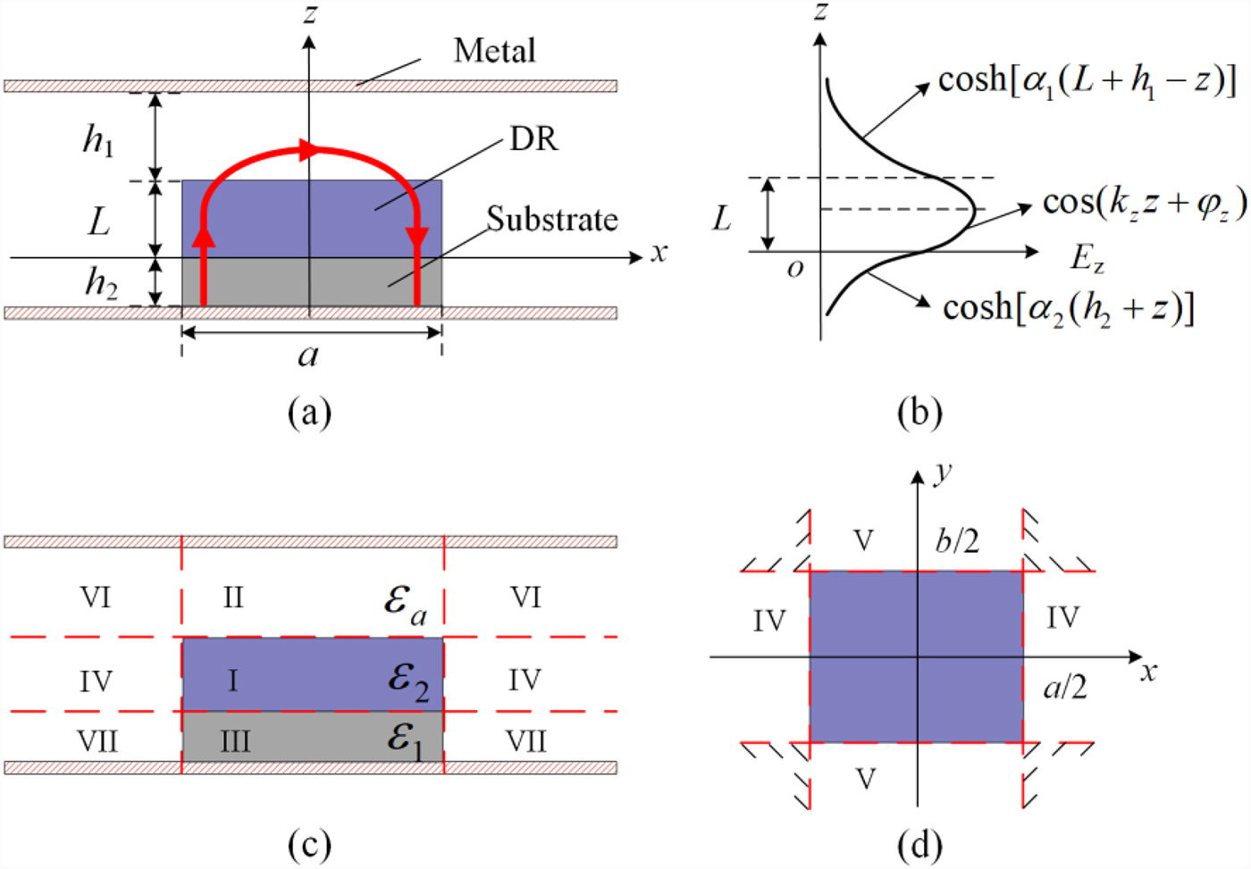
Fig. 2. The analysis model of the proposed PCB-based DR, (a) equivalent DR model with the TM11x mode E-field distribution sketch (red line), (b) the decay of the field along z-axis direction, (c) the front view of the regional division, (d) the top view of the regional division.
Here, the equivalent model which takes the regions of I–V into consideration is proposed. As a result, the complicated DR in Fig. 1 is converted to a traditional DR for solving the TM mode, which can be expressed as
 $$\left\{ \matrix{E_x = \displaystyle{1 \over {k^2 + \gamma_z^2}} \displaystyle{{\partial^2E_z} \over {\partial x\partial z}},\quad E_y = \displaystyle{1 \over {k^2 + \gamma_z^2}} \displaystyle{{\partial^2E_z} \over {\partial y\partial z}} \hfill \cr H_x = \displaystyle{{\,j\omega \varepsilon} \over {k^2 + \gamma_z^2}} \displaystyle{{\partial E_z} \over {\partial y}},\quad H_y = -\displaystyle{{\,j\omega \varepsilon} \over {-k^2 + \gamma_z^2}} \displaystyle{{\partial E_z} \over {\partial x}} \hfill} \right.,$$
 $$ \hskip-11pt \left\{ \matrix{E_{ZI} = A_1\cos (k_xx + \varphi_x)\cos (k_yy + \varphi_y)\cos (k_zz + \varphi_z) \hfill \cr E_{ZII} = A_2\cos (k_xx + \varphi_x)\cos (k_yy + \varphi_y)\cosh \alpha_1(L + h_1-z) \hfill \cr E_{ZIII} = A_3\cos (k_xx + \varphi_x)\cos (k_yy + \varphi_y)\cosh \alpha_2(h_2 + z) \hfill \cr E_{ZIV} = A_4e^{-\alpha_3(\vert x \vert -a/2)}\cos (k_yy + \varphi_y)\cos (k_zz + \varphi_z) \hfill \cr E_{ZV} = A_5\cos (k_xx + \varphi_x)e^{-\alpha_4(\vert y \vert -b/2)}\cos (k_zz + \varphi_z) \hfill} \right.,$$
 $$\left\{ \matrix{k_x^2 + k_y^2 + k_z^2 = \varepsilon_{\rm 2}k_0^2 \hfill \cr k_x^2 + k_y^2 -\alpha_1^2 = \varepsilon_ak_0^2 \hfill \cr k_x^2 + k_y^2 -\alpha_2^2 = \varepsilon_1k_0^2 \hfill \cr -\alpha_3^2 + k_y^2 + k_z^2 = \varepsilon_ak_0^2 \hfill \cr k_x^2 -\alpha_4^2 + k_z^2 = \varepsilon_ak_0^2 \hfill} \right.,$$
where ε in (5) is the permittivity in vacuum, k is the wave number at corresponding mode frequency, and γ z is the propagation constant along z direction. In this design, the PCB-based DR with a square shape owns a pair of orthogonal degenerate modes, i.e. TM11x and TM11y. They have the same resonant frequency. For the TM11x mode (k y = 0), the resonant frequency can be calculated by
 $$ \left\{ \matrix{\alpha_1^2 = k_x^2 -\varepsilon_ak_0^2 \hfill \cr \alpha_2^2 = k_x^2 -\varepsilon_1k_0^2 \hfill \cr \alpha_3^2 = \alpha_4^2 -k_x^2 \hfill \cr \beta^2 = \varepsilon_2k_0^2 -2k_x^2 \hfill \cr k_xa = \pi -2\arctan \left( {\displaystyle{{k_x} \over {\alpha_3}}} \right) \hfill \cr k_zL = \arctan \left[ {\displaystyle{{\varepsilon_2\alpha_1} \over {\varepsilon_1k_z}}{\rm coth}(\alpha_1h_1)} \right] + \arctan \left[ {\displaystyle{{\varepsilon_2\alpha_2} \over {\varepsilon_1k_z}}{\rm coth}(\alpha_2h_2)} \right] \hfill} \right..$$
Figure 3 shows the calculated and the simulated resonant frequencies of the TM11 mode under different a and L. The difference between them is <3%, which can be attributed to the difference of the employed models for simulation and calculation. As shown in Fig. 2(c), the regions of VI and VII are considered in the high frequency structure simulator (HFSS) simulation while they are ignored in the calculation based on (8). Figure 4 shows the frequency against the lateral-extension length c of the substrate. As c increases, the frequency of TM11 mode drops.

Fig. 3. The calculated and the simulated TM11 resonant frequencies under different a and L, while ε 2 = 10.2, ε 1 = 6.5, h 1 = 1 mm, and h 2 = 0.635 mm are fixed.

Fig. 4. The frequencies of TM11 mode against c.
Filter design and results
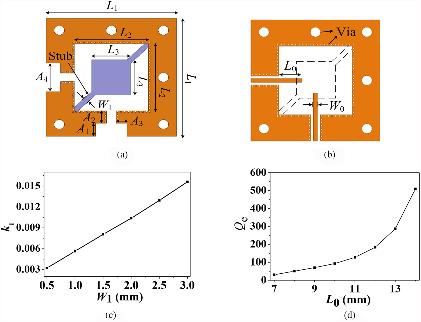
Figure 5(a) shows the layout of Substrate2 and the metal layer (M4) which is at the top of this substrate. The degenerate TM11 mode pair of the proposed PCB-based DR is orthogonal, which is fed by a pair of orthogonal strip lines in M5, as shown in Fig. 5(b). Accordingly, a pair of stubs with the width W 1 on the opposite corners in Substrate2 are not only used as the perturbations for splitting the two degenerate modes, leading to the mode coupling for building the passband, but also are useful for fixing and pinpointing the dual-mode DR. As W 1 increases, the frequency difference between the two modes is enlarged, i.e. the coupling level between them is enhanced, as shown in Fig. 5(c). Accordingly, the dual-mode filter is designed to be centered at 8.38 GHz (f 0). The 3-dB fractional bandwidth (FBW) of the passband is 1.64% and the 0.1 dB ripple FBW is 0.64%. Meanwhile, the return loss within the passband is about 20 dB. According to the specifications, the lumped-element values of a low-pass prototype filter can be calculated as g 1 = 0.60, g 2 = 0.51, and g 0 = 1. Then the required coupling coefficient k 1 and the external quality factor Q e can be obtained.
 $$k_1 = \displaystyle{{0.64\%} \over {\sqrt {g_1g_2}}} = 0.0116,\quad Q_e = \displaystyle{{g_0g_1} \over {0.64\%}} = 93.46.$$
Fig. 5. Design of the proposed filter, (a) layout of the Substrate2 and its top metal layer M4, (b) layout of the metal layer M5, (c) coupling coefficient k 1 against width of the stub W 1, (d) external quality factor Q e against the length of feeding line L 0.
The Q e is mainly determined by the length of the feeding line (L 0), which can be tuned for meeting the requirement of the desired Q e, as shown in Fig. 5(d).
The coupling mechanism of the proposed filter is shown in Fig. 6, where nodes S and L denote input and output ports, respectively. Nodes 1 and 2 represent the TM11x and TM11y modes which are a pair of degenerate modes. M S1 means the coupling strength between the input port and resonant mode TM11x, and M 2L represents the coupling strength between the TM11y mode and output port. M SL is the source-load coupling. The element M 12 in the coupling scheme can be obtained by the coupling coefficient k 1 between the TM11x and TM11y modes. As far as the nonresonating mode is concerned [Reference Bastioli, Tomassoni and Sorrentino4], it is coupled to both input and output ports, thus creating a direct input-to-output coupling. The filter employs both resonant and nonresonating modes so as to provide two reflection and two transmission zeros (TZs).

Fig. 6. Coupling scheme of the proposed dual-mode filter.
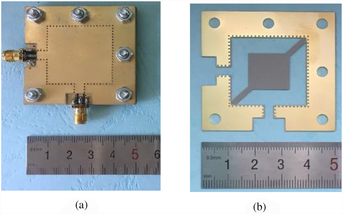
Based on the above discussion, the final dimensions of the filter are given as follows: L 0 = 10.2 mm, L 1 = 50 mm, L 2 = 30 mm, L 3 = 15 mm, W 0 = 1.6 mm, W 1 = 2 mm, A 1 = 5.5 mm, A 2 = 4.5 mm, A 3 = 4.2 mm, and A 4 = 12 mm. The simulated Q u of the resonator is about 700. Figure 7 shows the photograph of the fabricated filter. Figure 8 shows the simulated and measured results of the proposed filter, showing good agreement. The measured passband is cantered at 8.38 GHz with 3-dB FBW of 1.64%. In the passband, the measured minimum insertion loss (IL) is 1.1 dB (including SMA connector loss) and the return loss is better than 21.6 dB.

Fig. 7. The photograph of fabricated dual-mode DR filter, (a) overall structure, (b) Substrate2.
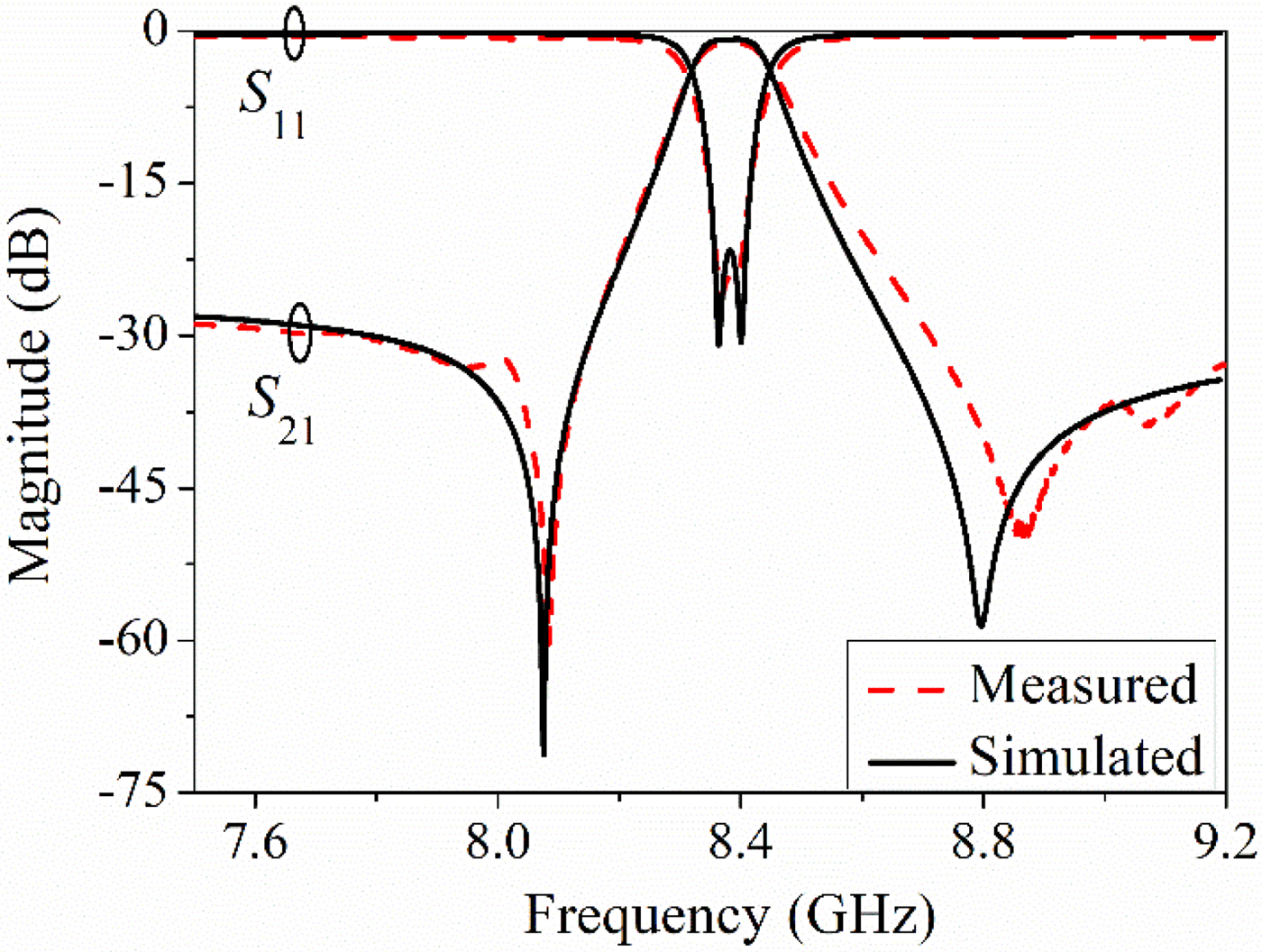
Fig. 8. Simulated and measured results of the proposed filter.
A comparison with the previous similar designs is summarized in Table 1. It can be found that the simulated Q u of the substrate-integrated suspended line (SISL) resonator also based on the similar multilayer PCB fabrication technology is still relatively low, resulting in large IL, which reaches 2.86 dB in the upper passband at 4.85 GHz. Similarly, the Q u of the SIW [Reference Cheng, Lin, Lancaster, Song and Fan9] is relatively low. As compared with the ESIW design in [Reference Belenguer, Esteban and Boria11], the proposed design has a smaller size. Meanwhile, the proposed PCB-based DR filter shows a low profile, as compared with the dielectric-strip design in [Reference Zhu, Li and Chen12]. The loss enlargement in this work is attributed to the narrower FBW. In a word, the proposed design owns several advantages such as compact size and relatively high Q u. Meanwhile, a pair of TZs are generated because the filter employs both resonant and nonresonating modes for improving selectivity of the passband.
Table 1. Performance comparison with other previous filters

Conclusion
In this paper, a substrate integrated dual-mode DR is constructed by using the multilayer PCB fabrication technology, and the resonant frequencies of the dominate modes are derived for designing X-band filter. Benefiting from the employment of the PCB-based DR with relatively high Q u, the filter possesses several advantages such as low loss, light weight, and compact size, which would be a good candidate in the current and future practical applications.
Author ORCIDs
Jian-Xin Chen, 0000-0002-8703-5294
Acknowledgement
The work was supported by Natural Science Foundation of Jiangsu Province, China (Grant No. BK20161281).
 Xiao-Xiao Yuan was born in Nantong, Jiangsu Province, China, in 1994. He received the B.Sc. degree from Nantong University, Nantong, in 2016. He is currently pursuing the M.Sc. degree in electromagnetic field and microwave technology in Nantong University, Nantong, China. His current research interests include antennas, microwave filters, and baluns.
 Li-Heng Zhou was born in Nantong, Jiangsu Province, China, in 1981. He received the B.Sc. degree from Nanjing University of Information Science and Technology, China, in 2004, the M.Sc. degree from Nanjing University of Science and Technology, China, in 2007. He has been with Nantong University, Nantong, China, since 2007. He has authored or co-authored 10 international journal or conference papers. He holds four Chinese patents. His research interests include RF/microwave components and subsystems.
 Jian-Xin Chen received the B.S. degree from Huai Yin Teachers College, Huai'an, China, in 2001, the M.S. degree from the University of Electronic Science and Technology of China (UESTC), Chengdu, China, in 2004, and the Ph.D. degree from the City University of Hong Kong, Hong Kong, in 2008. Since 2009, he has been with Nantong University, Nantong, China, where he is currently a Professor. He has authored or co-authored more than 100 academic papers. He holds 15 Chinese patents and three US patents. His research interests include RF/microwave differential circuits and antennas, dielectric resonator (DR) filters, and low temperature co-fired ceramic circuits and antennas. Dr. Chen received the Best Paper Award presented at the Chinese National Microwave and Millimeter-Wave Symposium, Ningbo, China, in 2007. He was the Supervisor of 2014 iWEM student innovation competition winner in Sapporo, Japan.