


I. INTRODUCTION
In this paper we address the targets of high energy efficiency over wide dynamic range signals along with wide operation bandwidth for high power amplifier (PA) design [Reference Kim, Junghwan and Kim1]. In the literature, both these problems are addressed separately by several design techniques [Reference Cripps2, Reference Cidronali, Mercanti, Giovannelli, Maddio and Manes3]. The most investigated PA architectures, capable of providing a wide dynamic range and sufficient operative bandwidth, are still those referring to the envelope tracking (ET-PA) [Reference Cidronali, Giovannelli, Magrini and Manes4–Reference Cidronali, Giovannelli, Vlasits, Hernaman and Manes7], and to the Doherty (DPA) [Reference Kim, Kim, Kim and Ha8]. Among these, the DPA represents a good candidate for the roll-out of new infrastructure equipment due to its reduced impact on the existing base station architecture [Reference Ladebusch and Liss9]. Nevertheless, the DPA technique still needs significant effort to meet the requirements of RF bandwidth and linearity imposed by the commercial wideband telecommunication applications. Indeed, the DPA is conventionally adopted for narrow band applications, where the main objective is the improvement of the average efficiency for high dynamic range modulated signals. With the above motivation, recent literature addresses the topic of the effective exploitation of the DPA concept over wide radio frequency (RF) bands.
The adoption of innovative device technologies like Gallium Nitride (GaN) represents a significant technological asset for many RF and microwave applications [Reference Bathich and Boeck10–Reference Chuanhui, Wensheng, Shihai, Chaojin and Youxi12]. Although GaN-based DPA permits high frequency (above 2 GHz) with wideband operation, and GaN devices on Silicon substrate are promising for lower cost, significant technological efforts are needed before they could be exploited in the below 1-GHz terrestrial digital video broadcasting (DVB-T) applications, which are addressed in this paper. In this respect, a cost-effective device technology for RF broadcasting applications is represented by the Silicon laterally diffused metal oxide semiconductor (LDMOS) device technology [Reference Moronval, Abdoelgafoer and Déchansiaud13], mainly due to its high gain (20 dB at 2 GHz), good efficiency, inherent linearity, excellent reliability, ruggedness, and low cost [Reference Theeuwen and Qureshi14]. These features make LDMOS the technology of choice for the development of DPA for broadcasting applications. This work is motivated by the experimental validation of the above assessment. We introduce a broadband DPA design technique that permits the coverage of wide fractional bandwidths like that in use in ultra high frequency (UHF) band DVB-T, with high average output power level and high energy efficiency.
In [Reference Giovannelli15] we investigated a new impedance inverter topology, in which the quarter-wave transmission line (QWTL) impedance inverter is replaced by a broadband multistage transformer capable of absorbing the device's parasitic capacitances. While the multistage impedance transformer has an inherent broad band operation as an impedance inverter, it introduces a bandwidth limitation when considered for peak-power operation, in which the load modulation at the summing node should be transferred to the main power device output. On the other hand, this issue occurs in those approaches that, focusing on the broad band increasing of the back-off operation, neglect the correct load modulation at peak power across the target bandwidth. The work proposed in [Reference Giovannelli15] extends the concept of PA devices' output capacitance absorption [Reference Qureshi, Li, Neo, van Rijs, Blednov and de Vreede16], by introducing a multi-stage impedance inverter designed over a wide bandwidth by a bi-objective optimization, capable of getting the best trade-off between the back-off and peak power DPA operations.
In this paper we further develop the approach proposed in [Reference Giovannelli15] by introducing a technique based on the splitting of the single-stage QWTL into two sub-networks and their subsequent implementation by appropriate pi-networks capable of absorbing the main device output parasitic capacitance. We show that this technique leads to an impedance inverter, suitable for DPA back-off operation fractional bandwidth, which is wider than the one associated with ideal QWTL, namely 54% versus 28%. As a direct consequence, it results in a wider DPA operation bandwidth for those RF power device technologies that exhibit higher capacitance per power density, where more conventional approaches would fail in delivering the performance across a wide bandwidth.
The paper is organized as follows. In Section II we analyze the DPA principle of operation, focusing on the factors limiting its operational bandwidth, and providing an average drain efficiency (DE) benchmark as a function of the signal dynamic. These factors are then reconsidered to introduce the direct synthesis of the impedance inverter in Section III. In Section IV the design of the DPA prototype suitable for DVB-T is provided and discussed, while its characterization is provided in Section V.
II. BROADBAND DPA LIMITATIONS
A) Principle of operation
The architecture of the DPA [Reference Kim, Kim, Kim and Ha8] exploits the mechanism of active load modulation, which is provided by the peak device over the main device. Indeed, in the so called back-off state the main device output termination at fundamental frequency is 2·R opt , where R opt is the optimum load at peak power for the main device, at its intrinsic current generator. This termination is provided by transforming, with an impedance inverter, the termination R opt /2 seen at the summing node toward the external load. In conventional designs, the impedance inverter is implemented by a QWTL, with characteristic impedance equal to R opt . When driven in the saturated state, the peak device provides an additional current into the output termination, thus making the effective main device's termination decrease from 2·R opt to R opt . In this state, the main device is saturated and its output voltage remains constant through the entire region. In saturation, the main device can be modeled by a voltage source and its output impedance is thus transformed into an open circuit at the summing node, as shown in Fig. 1.

Fig. 1. Schematic representation of the RF power devices combination at the output of the DPA operating in the saturation state.
The conventional design approaches consider the peak device biased in class-C operation to maintain its off state in the entire back-off DPA state. Despite this bias difference, in principle, the two devices at peak power would drive the same fundamental component current; thus, at a first analysis, the same output termination would be required and the same power would be generated by the two devices. In practice, due to the reduced conduction angle of the peak device, a reduced current at fundamental is generated, so a lower load termination is required for the peak device [Reference Kang, Kim, Cho, Park, Kim and Kim17]. Thus, this justifies the peak device matching network shown in Fig. 1. In addition, the latter network ensures that the peak device provides its due current into the summing node and thus enables the correct load modulation.
The described DPA operation principle exhibits at least two limiting factors for its effective exploitation. The first limiting factor consists in the inherent behavior of the QWTL impedance inverter, which significantly limits the bandwidth at back-off (transformation from R opt /2 to 2·R opt ). The second consists in the interaction between the QWTL and the parasitic capacitors, which decreases the bandwidth for both back-off and peak power states; this becomes significant for DPA with large high-power devices. These limiting factors are quite well addressed in the literature [Reference Qureshi, Li, Neo, van Rijs, Blednov and de Vreede16], and the proposed solutions consider the compensation of the RF device's output capacitor and new topologies of the output networks [Reference Piazzon, Giofre, Colantonio and Giannini11, Reference Yu-Ting, Annes, Bokatius, Kravavac and Tucker18]. Yet in all these cases the expected fractional bandwidth for continuous wave (CW) signals at DPA back-off is hardly larger than 28%. In order to increase the bandwidth, new approaches to the design of the output combiner were introduced in the literature [Reference Qureshi, Sneijers, Keenan, de Vreede and van Rijs19]. These approaches are aimed at increasing the bandwidth of the impedance inverter and concentrating the efforts on the operation of the DPA at back-off. The completely different approach proposed in [Reference Gustafsson, Andersson and Fager20], instead considers to design the impedance inverter with a characteristic impedance equal to R opt , thus making the DPA operation at back-off independent of frequency. The approach requires a proper amplitude and phase control of both the main and peak driving, which in [Reference Gustafsson, Andersson and Fager20] was implemented by an additional vector modulator.
B) DPA limitation to broadband modulated signals operation
We evaluate now the expected operative bandwidth of an ideal DPA, based on a conventional QWTL impedance inverter, as a function of exciting modulated signal peak-to-average power ratio (PAPR).
Let us assume the schematic representation of the DPA output network in Fig. 2, where the main and peak devices are represented by two current sources having fundamental output currents I m and I p that depend on the input voltage drive level 0 ≤ ξ ≤ 1,
 $${I_m} = \xi \displaystyle{{{I_{max}}} \over 2},$$
 $${I_p} = \left\{ {\matrix{ \hskip-42pt0 & {{\rm 0} \le \xi \le {\xi _{bo}}} \cr {\displaystyle{{{I_{max}}} \over 2}\displaystyle{{\xi - {\xi _{bo}}} \over {{\xi _{bo}}}}} & {{\xi _{bo}} \le \xi \le 1} \cr } } \right.,$$
where ξ bo = 0.5 is the drive level at the onset of the peak device and Imax is the maximum current of both the main and peak devices, assumed to be equal. The voltage at the summing node (node P in Fig. 2) can be evaluated by the 2-port analysis between the nodes “M” and “P” by considering the QWTL characterized by its Z-parameter matrix [Reference Qureshi, Li, Neo, van Rijs, Blednov and de Vreede16]. In order to calculate the DPA efficiency, we first calculate the output power, which after a simple manipulation and using (1) and (2) reads
 $${P_{out}} = \displaystyle{{V_{ds}^2} \over {{R_{opt}}}} \cdot \left\{ {\matrix{ {\displaystyle{{{{(\xi \cdot {\xi _{bo}})}^2}} \over {{{\cos} ^2}(\bar f) + {\xi _{bo}}{{\sin} ^2}(\bar f)}}{\rm, 0} \le \xi \le {\xi _{bo}}} \cr {\displaystyle{{{{\left \vert \matrix{\xi {\xi _{bo}} + (\xi - {\xi _{bo}}){\cos ^2}(\bar f) \hfill \cr \quad (\cos (\bar f) - j\sin (\bar f)) \hfill} \right \vert} ^2}} \over {{{\cos} ^2}(\bar f) + {\xi _{bo}}{{\sin} ^2}(\bar f)}}{\rm,} {\xi _{bo}} \lt \xi \le 1} \cr}} \right.,$$
where the normalized frequency
 $\bar f$
is defined as πf/2f
0 with the design center frequency. The (3) is valid under the assumption of QWTL designed at f
0 with characteristic impedance Z
c
= R
opt
and back-off drive level ξ
bo
= 0.5. The DC power consumption under the simplifying assumption that the peak device operates in mild class-C reads
$\bar f$
is defined as πf/2f
0 with the design center frequency. The (3) is valid under the assumption of QWTL designed at f
0 with characteristic impedance Z
c
= R
opt
and back-off drive level ξ
bo
= 0.5. The DC power consumption under the simplifying assumption that the peak device operates in mild class-C reads
 $${P_{DC}} = \displaystyle{{{V_{ds}}( \vert {I_m} \vert + \vert {I_p} \vert )} \over \pi}. $$
Combining (3) and (4), we can finally derive the DPA DE, DE = P out /P DC, which is drawn in Fig. 3 as a function of the drive level ξ, and the fractional bandwidth |f − f 0|/f 0. From the figure, we observe that the curves spread more at back-off (i.e. ξ bo = 0.5), thus determining the worst case for the DE bandwidth; in this state, only at center frequency and for the CW signal at the back-off level, the DPA exhibits the peak DE. Instead, at peak power all the curves converge at the peak DE, thus determining a significant contribution for those signals having low PAPR.

Fig. 2. Schematic representation of the DPA output network; the main and peak devices are represented by two ideal controlled current sources.

Fig. 3. DE for an ideal DPA implemented with a QWTL impedance inverter designed at f 0 with Z c = R opt , as a function of the fractional bandwidth |f − f 0|/f 0, and drive level ξ.
Let us now assume a drive signal having a level probability distribution function characterized by the Rayleigh distribution
 $$pdf(\xi ) = \displaystyle{\xi \over {{\sigma ^2}}}{e^{ - ({\xi ^2}/2{\sigma ^2})}},$$
where the parameter σ is related to the linear PAPR by
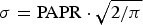 $\sigma = {\rm PAPR} \cdot \sqrt {2/\pi} $
. By integrating the curves in Fig. 3 weighted by (5), for the same signal peak power, we derive the average DE as a function of the fractional bandwidth,
$\sigma = {\rm PAPR} \cdot \sqrt {2/\pi} $
. By integrating the curves in Fig. 3 weighted by (5), for the same signal peak power, we derive the average DE as a function of the fractional bandwidth,
 $$\left\langle {DE} \right\rangle = \int\limits_0^1 {DE(\xi, \overline f ) \cdot pdf(\xi, \!\sigma )} \cdot d\xi. $$
The results of the numerical integration of (6) are shown in Fig. 4. In the same figure we include for comparison the result of the calculated average DE for a CW signal at back-off (i.e. the input level of the onset for the peak device), as a function of the normalized frequency, f/f 0. From the data we can calculate the bandwidth following the accepted criteria of 10% relative average DE drop at the band edge. The calculated bandwidth along with the maximum average DE is reported in Table 1. The bandwidth exhibits a significant reduction moving from PAPR = 3 dB to PAPR = 6 dB, while for higher PAPR it remains almost constant. Differently, the maximum of the average DE at the nominal design frequency, f 0, shows an almost linearly decreasing trend as the PAPR increases. The data relative to the CW signal at back-off confirm that the DPA DE bandwidth equals the QWTL bandwidth.

Fig. 4. Average DE performance for an ideal DPA, versus normalized frequency f/f 0, for modulated signals at different peak-to-average ratio (PAR) and same peak power. For comparison it is also reported the case of CW signal at back-off power.
Table 1. Bandwidth and average DE for ideal DPA.

It is worth highlighting that the results in Table 1 consider ideal devices, and we discuss hereinafter that the devices' output capacitance reduces significantly the bandwidth of the impedance inverter, also when a wideband absorbing technique is adopted [Reference Qureshi, Li, Neo, van Rijs, Blednov and de Vreede16]. The proper absorption of the main device parasitic is discussed in the next section.
III. THE BROADBAND SYNTHETIC MULTI-LINE IMPEDANCE INVERTER
A) Synthetic transmission lines properties
The synthesis of the proposed new wideband impedance inverter by transmission lines of proper lengths and shunt lumped elements is straightforward. With reference to Fig. 5, let us consider respectively Z 0 and θ 0 the characteristic impedance and the electrical length of a reference transmission line, and the corresponding transformed pi-network, composed of a transmission line having the characteristic impedance and the electrical length respectively Z 1 and θ 1, and being B S the shunt susceptance connected at both its ends. The ABCD matrix of the reference transmission line is
 $$\left \vert {\matrix{ {\cos ({\theta _0})} & {j{Z_0}\sin ({\theta _0})} \cr {j{Y_0}\sin ({\theta _0})} & {\cos ({\theta _0})} \cr}} \right \vert, $$
while the corresponding one associated to the pi-network is
 $$\left \vert {\matrix{ {\cos {\theta _1} - {Z_1}{B_S}\sin {\theta _1}} & {j{Z_1}\sin {\theta _1}} \cr {j\sin {\theta _1}(1 - {{({Z_1}{B_S})}^2} + 2{Z_1}{B_S}\cot {\theta _1})} & {\cos {\theta _1} - {Z_1}{B_S}\sin {\theta _1}} \cr}} \right \vert, $$
assuming B S = ω C p , with C p the parasitic capacitor to be absorbed, between these parameters the following relations hold:
 $$\omega \cdot {C_P} = \displaystyle{{\cos ({\theta _0}) - \cos ({\theta _1})} \over {{Z_0}\cos ({\theta _1})}},$$
 $${Z_1} = {Z_0}\displaystyle{{\sin ({\theta _0})} \over {\sin ({\theta _1})}}.$$

Fig. 5. Transmission line equivalence with a pi-network.
From (9) we see that for large capacitance values we get very short line lengths with corresponding high characteristic impedance. This combination of parameters makes the transmission line synthesis impractical. Furthermore, the equivalence is exact only at a single frequency, making the bandwidth of the loaded line narrower than the original unloaded line. From the above considerations, it results that in practical applications the device technology determines the maximum RF bandwidth. In particular, the ratio between the output capacitance and peak power is a figure of merit of several device suppliers in GaN and LDMOS technologies. For GaN technology this figure is in the range of 0.05 pF/W, while for LDMOS-based 50 V technology this figure ranges about 0.14 pF/W [Reference Ahmed21]. Thus, as expected, GaN technology provides the conditions for the wider bandwidth [Reference Chuanhui, Wensheng, Shihai, Chaojin and Youxi12]. Nevertheless, the LDMOS technology is still the best suited for high power at the lower frequency band, mainly due to the high ruggedness, low thermal resistance and good efficiency performance. The latter consideration motivates the effort in the development of broadband DPAs for DVB-T in the UHF band [Reference Qureshi, Sneijers, Keenan, de Vreede and van Rijs19].
For the design of the impedance inverter, we introduce a new concept that does not require complex multi-objective optimization and allows the impedance inverter function across a bandwidth that is wider than in ideal QWTL. In the treatment that follows, the parasitics are considered to be constant across the entire signal dynamic range, although not necessarily identical for the two devices. We can rewrite (9) in the more general form
 $${b_S} = \displaystyle{{{B_S}} \over {{Y_0}}} = \displaystyle{{\cos ({\theta _0}) - \cos ({\theta _1})} \over {\cos ({\theta _1})}},$$
where b S represents the shunt element at the ends of the transmission line. From (11) it results that if θ 0 < θ 1, i.e. when the line is shortened, the shunt element is positive, meaning a capacitive susceptance, while the case of elongation, θ 0 > θ 1, implies a negative, inductive susceptance.
The corresponding characteristic impedance is modified according to (10). In Fig. 6 we report a view of the line transformation expressed by (11), where the isoclines are associated with the shunt susceptance of the synthetic line. From the figure, it is evident that, starting from the reference electrical length, a transmission line can be either lengthened or shortened as long as the appropriate susceptance is shunted at the line ends, and the transformed impedance Z
1 remains feasible. For instance, having selected a cascade of two transmission lines, namely TL
a
and TL
b
, with nominal electrical length
 $\theta \hskip 1pt_0^A $
= 40° and
$\theta \hskip 1pt_0^A $
= 40° and
 $\theta \hskip 1pt_0^B $
= 10°, we can consider their implementation by a shorter transmission line tl
a
, of electrical length 20°, and a longer one, tl
b
, of 20°. The electrical length frequency dependence of the two nominal lines in the 450–850 MHz bandwidth is also reported in Fig. 6, and from their intersections with the isoclines, we can evaluate the resulting |b
S
|. Although the shunt susceptance values are not constant across the entire frequency range, the two trends are almost identical in absolute value. The advantage of this transformation is clear: since jBa and jBb follow almost the same path, they are intrinsically resonating over a broad band, thus giving a wide band equivalent line.
$\theta \hskip 1pt_0^B $
= 10°, we can consider their implementation by a shorter transmission line tl
a
, of electrical length 20°, and a longer one, tl
b
, of 20°. The electrical length frequency dependence of the two nominal lines in the 450–850 MHz bandwidth is also reported in Fig. 6, and from their intersections with the isoclines, we can evaluate the resulting |b
S
|. Although the shunt susceptance values are not constant across the entire frequency range, the two trends are almost identical in absolute value. The advantage of this transformation is clear: since jBa and jBb follow almost the same path, they are intrinsically resonating over a broad band, thus giving a wide band equivalent line.

Fig. 6. Plot describing the normalized shunt susceptance needed to either shrink (red line) or lengthen (blue line) a transmission line with electrical length θ 0.
It is remarkable that around the central area the isoclines exhibit similar slope, converging to exactly 45° for the particular condition θ 0 = θ 1, which implies no-transformation. About this line, the isocline curvature is mildly variable, meaning that for small length variation, the susceptance is almost invariant with respect to the ratio θ 1/θ 0. Opposite isoclines corresponding to ±b S show the same distance from the bisect line, which is a hint of a natural balance between the two kinds of transformation. It has to be clarified that the analysis carried out is frequency-dependent. Thus, if the shunt susceptance for the synthetic line is implemented by either a capacitor or an inductor, the bandwidth of the transformed line is in principle narrow band.
B) Synthetic multi-line impedance inverter design
The frequency behavior dualism of both the transformations discussed in the previous section, and the inherent bandwidth limitation, due to the presence of the output devices parasitic capacitance that load the impedance inverter, suggest a different way to operate, which is discussed hereinafter.
Let us consider the conventional impedance inverter based on a QWTL, and assume it is divided into two parts, namely TL
a
and TL
b
, as depicted in Figs 7(a) and 7(b). With reference to this arrangement, the transmission line TL
a
is made shorter, tl
a
in the Fig. 7(b), with the electrical length moved from
 $\theta \hskip 1pt_0^A $
to
$\theta \hskip 1pt_0^A $
to
 $\theta \hskip 1pt_1^A $
with
$\theta \hskip 1pt_1^A $
with
 $\theta \hskip 1pt_0^A $
>
$\theta \hskip 1pt_0^A $
>
 $\theta \hskip 1pt_1^A $
, while the transmission line TL
b
is made longer, tl
b
in the Fig. 7(b), with
$\theta \hskip 1pt_1^A $
, while the transmission line TL
b
is made longer, tl
b
in the Fig. 7(b), with
 $\theta \hskip 1pt_0^A $
<
$\theta \hskip 1pt_0^A $
<
 $\theta \hskip 1pt_1^A $
. According to Fig. 6, it is then possible to select the new lengths
$\theta \hskip 1pt_1^A $
. According to Fig. 6, it is then possible to select the new lengths
 $\theta \hskip 1pt_1^A $
and
$\theta \hskip 1pt_1^A $
and
 $\theta \hskip 1pt_1^B $
Z such that the required two susceptances are opposite, jBa = −jBb, and thus compensate each other. It is easy to demonstrate that the opposite susceptances lead to the condition:
$\theta \hskip 1pt_1^B $
Z such that the required two susceptances are opposite, jBa = −jBb, and thus compensate each other. It is easy to demonstrate that the opposite susceptances lead to the condition:
 $$\left \vert {{b_S}} \right \vert = \displaystyle{{\cos (\!\theta \hskip 1pt_1^A ) - \cos (\!\theta \hskip 1pt_0^A )} \over {\cos (\!\theta \hskip 1pt_0^A )}} = \displaystyle{{\cos (\!\theta \hskip 1pt_1^B ) - \cos (\!\theta \hskip 1pt_0^B )} \over {\cos (\!\theta \hskip 1pt_0^B )}},$$
which implies a further condition for the overall length:
 $${\theta _0} = \theta \,_0^A + \theta \,_0^B. $$

Fig. 7. Schematic description of the synthetic implementation of the impedance inverter (a) by two transmission lines (b) and compensating the transistors' parasitic capacitor, C p (c).
While the characteristic impedances of the two splitting lines are the same:
 ${Z_0} = Z_0^A = Z_0^B $
, the characteristic impedances composing the synthetic lines
${Z_0} = Z_0^A = Z_0^B $
, the characteristic impedances composing the synthetic lines
 $Z_1^A $
and
$Z_1^A $
and
 $Z_1^B $
are dictated by (10). The splitting ratio in (13) results to be a degree of freedom leading to the proper |b
S
|, thus yielding the proper capacitance for the left end of the synthetic tl
a
line, being |b
S
| = ω·C
p
/Y
0 with C
p
the output device capacitance. In addition, the proper choice of the addends in (13) is driven by the constraint of feasibility of the characteristic impedance from (10). The synthetic impedance inverter design is completed by inserting a shunt inductor, L
p
, at the right end of the tl
b
|b
S
| = 1/ω·L
p
·Y
0. Because of (12), in practical implementation, two out of the four shunt lumped elements, namely the inner ones depicted in Fig. 7, cancel each other out and thus do not need to be implemented. The beneficial effect of this cancellation is the removal of the corresponding band limiting behavior. As both L
p
and C
p
are frequency-dependent, inserting them as a lumped element implies that their value would be estimated at the center band, which introduces the frequency limitation of the implementation. The splitting in (13) is regarded as a degree of freedom for the design of the synthetic impedance inverter.
$Z_1^B $
are dictated by (10). The splitting ratio in (13) results to be a degree of freedom leading to the proper |b
S
|, thus yielding the proper capacitance for the left end of the synthetic tl
a
line, being |b
S
| = ω·C
p
/Y
0 with C
p
the output device capacitance. In addition, the proper choice of the addends in (13) is driven by the constraint of feasibility of the characteristic impedance from (10). The synthetic impedance inverter design is completed by inserting a shunt inductor, L
p
, at the right end of the tl
b
|b
S
| = 1/ω·L
p
·Y
0. Because of (12), in practical implementation, two out of the four shunt lumped elements, namely the inner ones depicted in Fig. 7, cancel each other out and thus do not need to be implemented. The beneficial effect of this cancellation is the removal of the corresponding band limiting behavior. As both L
p
and C
p
are frequency-dependent, inserting them as a lumped element implies that their value would be estimated at the center band, which introduces the frequency limitation of the implementation. The splitting in (13) is regarded as a degree of freedom for the design of the synthetic impedance inverter.
C) Synthetic multi-line impedance inverter bandwidth properties
The plot of Fig. 6 includes the details for the specific implementation of a 600 MHz QWTL with characteristic impedance of 8 Ω. It is composed of the cascade two transmission lines, respectively, with electrical lengths of 65° and 25°, implemented by opposite strategies. The first is subject to shortening and results in a line having 17.79 Ω and an electrical length of 24.05° with a shunt susceptance of 67.66 mS at both the ends. The second line results from the lengthening of the nominal and exhibits a characteristic impedance of 4.59 Ω and an electrical length equal to 47.35°, with a shunt susceptance of 67.67 mS. Considering the center frequency of 600 MHz, the resulting structure is implemented by the topology shown in Fig. 8(a), where the shunt elements consist of a capacitor of 17.94 pF and an inductor of 3.92 nH, which is reduced to 2.91 nH to optimize the impedance inverter center frequency. In the actual implementation, the capacitor represents the device parasitic, or at least a part of it. The topology of the resulting impedance inverter is reported in Fig. 8 along with the topology of the compensated QWTL designed by the conventional capacitance absorbing method [Reference Qureshi, Li, Neo, van Rijs, Blednov and de Vreede16]. This latter can be considered as the benchmark of the proposed approach.

Fig. 8. Topology of the synthetic impedance inverter of this work (a), and compensated QWTL by shunt capacitors (b), both implementations considering the same center frequency of 600 MHz.
The Figs 9 and 10 show the comparison between the input impedance and reflection coefficient of the two networks in Fig. 8, along with that of the ideal QWTL (designed at 600 MHz with Z 0 = 8 Ω), when the output is terminated to both 4 and 8 Ω, respectively. These values represent the terminations involved in the prototype implementation introduced hereinafter in Section IV. All the impedance inverters have a characteristic impedance of 8 Ω, and are analyzed in the 400–800 MHz bandwidth. In particular, Fig. 9 reports the normalized real part of the input impedance in the frequency range 400–800 MHz for the transformation involved in the DPA back-off operation, i.e., 4–16 Ω. From the comparison we can evaluate the capability of the proposed network to operate in a fractional bandwidth of 54%, which is twice the bandwidth of the ideal QWTL, and significantly larger than the more feasible compensated QWTL, which is limited to 21%. The proposed network in the same frequency band exhibits a maximum phase rotation of +17° to −25° at the opposite bandwidth extremes. When considering the transformation from 8 to 8 Ω reported in Fig. 10, the ideal QWTL exhibits no band limitation, while in this case the proposed impedance inverter technique exhibits an operative bandwidth, which is comparable with the one exhibited by the compensated QWTL. These results justify the expected wider bandwidth DPA operation with respect to conventional implementations.

Fig. 9. Comparison between normalized simulated input impedances for the ideal QWTL, the compensated QWTL by shunt capacitors, and the impedance inverter of this work; transformation R L = 4 to 16 Ω.

Fig. 10. Comparison between input reflection coefficients for the ideal QWTL (designed at 600 MHz with Z 0 = 8 Ω), the compensated QWTL by shunt capacitors, and the impedance inverter of this work; transformation R L = 8 to 8 Ω, frequency range 400–800 MHz.
The synthetic impedance inverter capability to deal with modulated signal is numerically evaluated in the same conditions adopted in the Section IIB. An ideal DPA implementing the synthetic impedance inverter hereinabove discussed has been numerically analyzed, and the DE has been derived as a function of the drive level and carrier frequency; the results are reported in Fig. 11. According to the impedance inverter frequency behavior at the two fundamental states of the DPA, reported in Figs 9 and 10, we clearly observe different behavior with respect of the QWTL based impedance inverter. Namely, for the same fractional bandwidth values the DE results ranging between the maximum theoretical value of 78.5%, and a minimum of 54.6% at back-off, while a minimum of 31.4% is reached at peak power. It is worth to note that, in the case of QWTL at back-off the DE is 31.1% at the bandwidth limits. This is of dramatic importance for the performance of the DPA when driven by modulated signals with high PAPR.
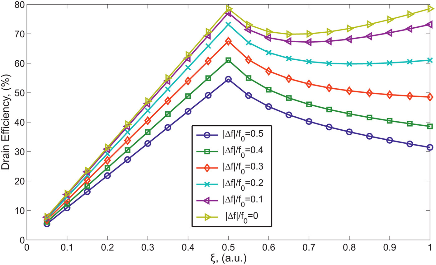
Fig. 11. DE for an ideal DPA implemented with the synthetic multi-line impedance inverter designed at f 0 with Z c = R opt , as a function of the fractional bandwidth |f − f 0|/f 0, and drive level ξ.
The DE reported in Fig. 11 has been integrated by the (6) maintaining the same peak power and the results are shown in Fig. 12, as a function of the normalized frequency, f/f 0. As in the previous case, from the data we can calculate the bandwidth following the accepted criteria of 10% relative average DE drop at the band edge. The calculated bandwidth, along with the maximum average DE is reported in Table 2. When compared with the data in Table 1 we observe that the average DE at the design frequency remains unvaried; for the case of PAPR = 3 dB the proposed technique leads to a reduction of performance, while from PAPR = 6 dB and higher the improvement of fractional bandwidth is significant, for instance, for PAPR = 9 dB the improvement is about the 16%.

Fig. 12. Average DE performance for an ideal DPA implementing the synthetic impedance inverter, versus normalized frequency f/f 0, for modulated signals at different peak-to-average ratio (PAR) and same peak power. For comparison it is also reported the case of CW signal at back-off power.
Table 2. Bandwidth and average DE for ideal DPA implementing the synthetic impedance inverter.

IV. BROADBAND DPA PROTOTYPE
The technique discussed hereinabove has been adopted for the design and the development of a prototype around Infineon's PTVA042502FC Si LDMOS transistor operating over 475–806 MHz. The devices are biased at 50 V. The main in quiescent state exhibits a drain current of 0.4 A, while the peak is in deep class-C operation. The architecture of the DPA prototype is schematically shown in Fig. 13, where the two-line impedance inverter is connected between the main device and the summing node, while, between the peak device and the summing node, a matching network adapts the common load impedance to the optimum impedance of the peak device. The impedance inverter is the one discussed in Section IIIB with its implementation reported in Fig. 8(a). Finally a multi-section broad band output matching network transforms the 50 Ω load to the optimum common termination at the summing node [Reference Fagotti, Cidronali and Manes22].

Fig. 13. Topology of the broadband DPA with synthetic multi-line impedance inverter.
The optimum device terminations are estimated by load-pull analysis, from which we estimate a total output parasitic capacitance C p = 25 pF. Assuming this value composed of two parts, C p = C p1 + C p2, (cfr. Fig. 13), a contribution of 18 pF is absorbed by the synthetic impedance inverter (see C p2 in Fig. 13), while a residual parasitic capacitor, C p1 = 7 pF, remains in parallel to the main device output. This choice is motivated by two needs: the first is related to the feasibility of the absorbing technique, which is ruled by the (9) and that imposes a maximum value of parasitic capacitance absorption given the frequency and the characteristic impedance of the nominal transmission line; the second factor is related to the beneficial effect on the DE of shorting the current harmonics. Instead, for the peak device, the load-pull analysis has been performed by considering the actual intrinsic device. The results of the two load-pull analyses are reported in Fig. 14, for the center frequency of 600 MHz. From the data we estimate an output delivered power of 51.5 dBm on the termination of 8.3 + j4.3 Ω for the main device, while for the peak device we estimate 50.4 dBm of delivered power on a load of 7 − j0.9 Ω. The difference between main and peak optimum impedances is due to the different operation.

Fig. 14. Load pull analysis at 600 MHz, for the main and peak devices considering a residual drain capacitor of 7 pF for the main device, while for the peak device the data are referred to the intrinsic device drain current generator.
The device output capacitance for the peak is estimated at 30 pF, with the bonding and package parasitic not significantly affecting this value; the package is taken into account for the design of the peak matching network design. For the purpose of the complete output combiner design, the summing node impedance is fixed at 4 Ω across the entire bandwidth. The output combining network, which includes the bias networks, the actual layout geometries, and the compensation of the residual parasitic capacitance, has been optimized starting from the two-line impedance inverter dimensioning depicted in Fig. 8(a). The use of a multi-objective routine optimizes the performance across the bandwidth by compensating the non-idealities of the transmission lines bend, their junctions and the package influence.
The resulting simplified schematic of the output network is shown in Fig. 15 along with the nominal values of the critical parts. In the figure, TL 1, TL 2 and L 1 along with part of the device parasitic implement the impedance inverter. In the same figure, TL 3 and L 2 implement the peak device matching network capable of transforming the optimum termination in Fig. 14 into the summing node common impedance, taking account of the device and package parasitics. The implementation of the circuit is on a plastic laminate substrate with dielectric constant ε r = 3.5 and 10 mils thickness. The simulated behavior in terms of CW DE across the bandwidth (not reported) shows that the peak power reaches 55 dBm with a DE of 65%. At 6 dB back-off, the DE reduces due to the imperfect operation of the impedance inverter, and for the same reason the DE shapes spread between 40 and 50%.

Fig. 15. Detailed schematic of the DPA output combiner. L 1 = 2.91 nH L 2 = 8.2 nH; TL 1: width/length 3.8/4.2 mm; TL 2: width/length: 4.5/1.6; TL 3: width/length: 8/4.3.
The input network provides a two-stage symmetric Wilkinson power divider, which enables more accurate control of the phasing between peak and main across the bandwidth. This network has been optimized to maximize the amplitude and phase-alignment between peak and main output currents at the summing node point at the maximum drive level. The amplitude mismatch of the designed input network is within 1.5 dB, while the nominal phase difference is 90 ± 15° across the bandwidth. In Fig. 16 we show the photograph of the assembled prototype, used for the RF test hereinafter introduced.

Fig. 16. Photograph of the DPA prototype based on the PTVA042502FC Si LDMOS operating in the 450–806 MHz range implementing the multi-line impedance inverter.
V. PROTOTYPE EXPERIMENTAL RESULTS
The characterization of the prototype considers both a pulsed CW characterization and a DVB-T signal composed of 8 k sub-carriers orthogonal frequency-division multiplexing (OFDM), with 64 quadrature amplitude modulation (QAM) and one channel with 8 MHz bandwidth. The input signal PAPR is 10.5 dB. The signal bandwidth of concern is the one referred to the broadcast application.
A) Large signal pulsed CW characterization
The pulsed CW characterization of the prototype is performed with an RF pulse width of 100 µs and 10% duty cycle; the resulting measured pulsed CW DE is reported in Fig. 17 as a function of the output power, across the 500–800 MHz bandwidth. The DE shows a peak of 62% at 53.9 dBm measured at 750 MHz, while the peak power of 54.9 dBm to which a DE of 54.5% corresponds is measured at 650 MHz. The DE reported in Fig. 17 at 6-dB output back-off spans form a minimum of 36.7% at 500 MHz to a maximum of 48.2% at 750 MHz. The Fig. 18 reports the power gain as a function of the output power, where a maximum is observed at all the measured frequencies. For the entire set of test frequencies, the gain expansion, due to a possible input mismatch of the main device, and the following compression are responsible of the observed reduction of the output power range, within which the DE remains about its maximum value.

Fig. 17. Measured DE versus output power in pulsed CW for several carrier frequencies.

Fig. 18. Measured power gain versus output power in pulsed CW for several carrier frequencies.
B) DVB-T modulated characterization
The test of the DPA prototype performance for DVB-T operation is carried out by the use of a DVB-T signal exciter. The set of input signals considers carriers spanning 475–850 MHz; the signal PAPR is 10.5 dB. All of the following data points are measured with a constant PAPR at the Doherty output of 7 dB, which corresponds to 3.5 dB of output level compression for each frequency point within the observed bandwidth. In Fig. 20 we report the corresponding average power as a function of the DVB-T carrier frequency. From the figure we observe that the maximum average power of 50.3 dBm is reached at 750 MHz, while across the bandwidth the average power remains within 49.3 dBm ± 1 dB. The values of the average power reported in the figure correspond to the maximum power at the prototype output, regardless of any other linearity concerns; in these cases the ACPR is slightly better than 20 dBc.

Fig. 19. Photograph of the broadband push-pull PA prototype designed by using the same device and adopted to benchmark the DPA prototype performance.

Fig. 20. Measured average output power as a function of the carrier frequency.
The corresponding values of the average DE are reported in Fig. 21. The maximum of 53% is obtained at 750 MHz, while the minimum of 40% is reached at 470 MHz. The 13% variation of the DE is considered an acceptable spread for practical applications; nevertheless, more effort in the optimization might lead to a flatter response. Recalling the theoretical analysis reported in Fig. 12 and summarized in Table 2 we observe that for PAPR = 10.5 dB an estimated average DE of 59.5% is expected, which should be considered as a performance benchmark , and represents an overestimation due to the non-idealities of the DPA not included in the analysis conducted in Section IIIC. The maximum shown in Fig. 21 results shifted at slightly higher frequency due to the effect of the DPA power gain, shown in Fig. 22, also shifted of the same amount due to imperfect matching of the input stage. The large signal power gain reported in Fig. 22 exhibits a maximum of 18 dB at 750 MHz and a behavior very similar to the trend seen for the DE, thus confirming that also the gain feature requires an optimization versus the frequency band.

Fig. 21. Comparison between measured average DE as a function of the carrier frequency for both the DPA and the push-pull prototypes developed with the same devices.
For a more comprehensive evaluation of the DPA performance, we provide the gain, DE and adjacent channel power ratio (ACPR) obtained by a push-pull PA designed using the same LDMOS device. The prototype photograph for the push-pull PA is provided in Fig. 19. The measured data for the DE, power gain and ACPR, under the same DVB-T excitation, are reported along with those of the DPA, respectively in Figs 21–23. The selection of a push-pull PA as a benchmark for the evaluation of the DPA design provided in this work is mainly motivated by the widely recognized characteristic of this design to provide a high-power level in a broad band due to the mechanism of doubling the output termination and thus reducing the output Q-factor of the output matching network. The comparisons show that the DE exhibited by the push-pull PA is constant across the bandwidth at about 28%, which is between 12 and 24% lower than the DPA prototype values. As expected, the inherent linearity of the DPA is worse than the raw linearity of the push-pull linearity. This is demonstrated by the ACPR raw data for the two prototypes shown in Fig. 23, which reports values for the push-pull that are on average 10 dB better than those of the DPA. These comparisons provide a qualitative, although meaningful, evaluation of the quality of the DPA design introduced in this paper.

Fig. 22. Comparison between measured gain as a function of the carrier frequency for both the DPA and the push-pull prototypes developed with the same devices.

Fig. 23. Comparison between measured ACPR as a function of the carrier frequency for both the DPA and the push-pull prototypes developed with the same devices.
C) Linearized DPA evaluation
The prototype is evaluated in a laboratory digital pre-distortion (DPD) platform supporting a bandwidth of 150 MHz. The platform consists of a vector signal generator for stimulus generation, a signal analyzer for capturing the feedback signal, and a host machine for system identification and stimulus pre-distortion using an indirect learning architecture implemented in MATLAB. The test signal adopted in the following set of experiments is the same as already presented in Section VB, though with different carrier amplitude levels in order to meet different energy efficiency versus linearity trade-offs. For all experiments, a generalized memory polynomial model [Reference Morgan, Ma, Kim, Zierdt and Pastalan23] of order 9 with memory 5 and envelope-lag 1 is used.
Two showcases are herein reported as representative of the prototype performance, and are of specific interest for the DVB-T applications. The first result, shown in Fig. 24, is a test with 60 W target power at a carrier frequency of 750 MHz. In this case, the output PAPR is equal to 7 dB and the DPD makes it possible to achieve better than −51 dBc of ACPR measured at 8 MHz offset. In this case, the total average output power is 47.8 dBm with a system average DE of 44.3%. It is worth to note that the power level is 2.5 dB lower than the average power reported in Fig. 20 for 3.5-dB of power compression. Before the application of the DPD the ACPR results −27.3 dBc, while for a better comprehension of the inherent DPA linearity, the AM/PM and AM/AM curve in the envelope domain are reported in the Fig. 25. The result of the second showcase, reported in Fig. 26, considers a high-linearity case with PAPR = 7.5 dB at the carrier frequency of 650 MHz. In this specific case, the output power is of 46.2 dBm with an ACPR of −58 dBc, while the resulting DE is 30.6%. For this test case, should be noticed that the power is 3.5 dB lower than the average power reported in Fig. 20. It results that, before the application of the DPD the ACPR results −33.73 dBc, while for a better comprehension of the inherent DPA linearity, the AM/PM and AM/AM curves in the envelope domain are reported in the Fig. 27. The discussed showcases demonstrate that the prototype is suitable for inclusion in a DPD platform with a significant expectation of linearity performance, while preserving output power and energy efficiency.

Fig. 24. Spectrum about the carrier of 750 MHz with memory digital pre-distortion; bandwidth = 7.61 MHz, output PAPR = 7 dB.

Fig. 25. AM/PM (a) and AM/AM (b) distortion for a DVB-T signal with carrier at 750 MHz before and after pre-distortion; with memory digital pre-distortion; bandwidth = 7.61 MHz, output PAPR = 7 dB and total channel power of 47.8 dBm.

Fig. 26. Spectrum about the carrier of 650 MHz with memory digital pre-distortion; bandwidth = 7.61 MHz, output PAPR = 7.5 dB.

Fig. 27. AM/PM (a) and AM/AM (b) distortion for a DVB-T signal with carrier at 650 MHz before and after pre-distortion; with memory digital pre-distortion; bandwidth = 7.61 MHz, output PAPR = 7.5 dB and total channel power of 46.2 dBm.
VI. CONCLUSION
The work presented in this paper has shown the development of a broadband LDMOS DPA, whose optimization is enabled by a two-line impedance inverter capable of absorbing most of the parasitic main device output capacitance. The measured performance with an 8 MHz DVB-T 10.5 dB PAPR signal has shown a 475–806 MHz bandwidth. Across the bandwidth, the PA exhibited more than 48.3 dBm of average output power with between 40 and 53% of average DE. Under the action of a memory DPD the prototype exhibits −52 dBc ACPR, with more than 60 W output power and 44.3% efficiency at the carrier frequency of 750 MHz. Both with and without DPD, the PA shows more than 50% efficiency enhancement compared with a standard class AB push-pull PA built around the same device. The prototype performances are compared in Table 3 with recently reported results for wideband DPAs in Si-LDMOS technology. From the Table we observe that [Reference Qureshi, Sneijers, Keenan, de Vreede and van Rijs19] and this work present the widest fractional bandwidth reported in the literature. In addition, with respect to [Reference Qureshi, Sneijers, Keenan, de Vreede and van Rijs19], which adopts a larger device, namely 700 W versus 280 W, this work reports a lower output power back-off with respect to the peak power, namely 6.7 dB versus 8 dB, and maintains simultaneously a better linearity, namely −52 dBc versus −45 dBc.
Table 3. Comparison with LDMOS Wideband DPA.

* Wideband envelope.
† Mixed-signal dual input drive.
 Alessandro Cidronali received his Laurea and Ph.D. degrees in Electronics Engineering from the University of Florence, Florence, Italy, in 1992 and 1997, respectively. From 1999 to 2011, he was an Assistant Professor with the Department of Electronics and Telecommunications, University of Florence. From 1999 to 2003, he was a Visiting Researcher with the Motorola Physics Science Research Laboratory. From 2002 to 2005, he was a Guest Researcher with the Non-Linear Device Characterization Group, Electromagnetic Division, National Institute of Standards and Technology (NIST). Under the frame of the IST-EU FP6 Network TARGET (IST-1-507893-NOE), he was Work package Leader for the transmitters modeling/architectures for wireless broadband access' work packages. He is currently an Associate Professor with the Department of Information Engineering, University of Florence, where he teaches courses on electron devices and integrated microwave circuits. His research activities concern the study of analysis and synthesis methods for nonlinear microwave circuits, the design of broadband microwave integrated circuits and the development of computer-aided design (CAD) modeling for microwave devices and circuits. He was recipient of the Best Paper Award presented at the 61st ARFTG Conference. From 2004 to 2006, he was an Associate Editor for the IEEE Transaction on Microwave Theory and Techniques. He is currently a member of the IEEE MTT-S TC-20 Wireless Communications and TC-27 Vehicular Technologies and Communications.
 Niccolò Giovannelli was born in Vienna, Austria, in 1984. He received his Master Degree (cum laude) in Electronic Engineering from the University of Florence, in 2007, and his Ph.D. in RF, Microwaves and Electromagnetics in 2011 from the same University. From 2008 to 2011 he has been working at Nujira Ltd. in Cambridge, UK, developing high efficiency Envelope Tracking Power amplifiers for Base Stations, TV broadcast and military applications. From 2011 to 2014 he has worked for Infineon Technologies in Munich, Germany, as Senior RF Applications Engineer for RF power transistors in both LDMOS and GaN technologies. He is currently working for Infineon Technologies Americas based in California, San Jose', as Cellular Applications Engineering Manager. Since 2007 he has being actively collaborating with Miclab within the Department of Electronics and Telecommunications of the University of Florence. His research interests include high-efficiency RF power amplifier design, RF systems and advanced transmitter architectures for future base-stations and RF power applications.
 Stefano Maddio was born in Florence, Italy on September 3, 1978. Graduated in Electronic Engineering at the University of Florence in 2005, he received Ph.D. with a thesis entitled “Circularly Polarized Smart Antennas for Wireless Sensor Network Devices” in 2009 and then he joined the staff of Microelectronic laboratory (Department of Electronics and Telecommunications) at University of Florence. His research activities cover both the electromagnetic and electronic topics of the microwave engineering, such as the analysis and design of radiative systems for microelectronics in the field of smart antenna technology for wireless applications, with particular emphasis on the issues of wireless localization and special-purpose antenna systems for Dedicated Short Range Communications. His scientific interests also cover the area of signal elaboration and manipulation at front-end level, with particular emphasis on active and passive filtering and noise mitigation as well as numerical techniques for free and guided electromagnetic propagation.
 Andrea Del Chiaro was born in Florence, Italy, in 1988. He received his Master degree (cum laude) in Electronic Engineer from the University of Florence, in 2014, and he is currently working in Infineon Technologies Austria. In 2014 he joined the Application Engineers Team of the RF Power group of Infineon Technologies, in Munich, Germany, after he developed his Master thesis work about a broadband Doherty power amplifier. From 2015 he is located in Villach, Austria, where he is involved in the design of high-efficiency power amplifier (e.g. Doherty amplifiers) for base-station telecommunication. His research interests include high-efficiency RF power amplifier design, RF systems and advanced transmitter architectures for future base-stations and RF power applications.
 Christian Schuberth received his Dipl.-Ing. degree from the Technical University in Vienna in 2004. From 2004 to 2010 he was with the Microwave Engineering Group at the Institute for Electrical Measurements and Circuit Design (TU Vienna) where he was involved in the design and testing of efficient and linear microwave power amplifiers and non-linear device characterization. Since 2010 he is with Infineon Technologies Austria, where he is currently working as a design engineer for wireless communication applications. He is a member of the IEEE. His research interests include highly efficient and linear power amplifiers as well as non-linear device measurement systems.
 Thomas Magesacher received his Dipl.-Ing. degree in Telematics from Graz University, Austria, the Ph.D. degree in Signal Processing from Lund University, Sweden, and the Docent degree in Telecommunications from Lund University, Sweden, in 1998, 2006, and 2011, respectively. During 2007–2008, he spent a year as postdoctoral fellow at the Department of Electrical Engineering, Stanford University, CA. Since 2011, he holds an Associate Professor position at the Department of Electrical and Information Technology, Lund University, Sweden. He has (co)authored about 70 papers in international journals, conference proceedings, and edited books as well as 15 patents. He has been and is working in close cooperation with the semiconductor and telecommunications industry both as staff member and in consulting roles. His research interests include applied information processing and optimization for communications. He received the 2008 Ingvar Carlsson Award from the Swedish Foundation for Strategic Research. He is a co-recipient of two IEEE International Conference on Communications (ICC) best paper awards (2014, 2015) and two best paper awards form the IEEE Communications Society's Transmission, Access, and Optical Systems (TAOS) Technical Committee (2014, 2015).
 Peter Singerl received his M.Sc and Ph.D. degrees in Telematics and Electrical Engineering from Graz University of Technology, Austria, in 2000 and 2006, respectively. From August 2003 to March 2007, he was with the Christian Doppler Laboratory for Nonlinear Signal Processing at the Graz University of Technology Austria. He joined Infineon Technologies Austria in August 2000, where he is currently working as a Principal concept engineer and manager for wireless communication applications. His research interest includes the identification and linearization of power amplifiers as well as system concepts for radio frequency transceivers. He has received two international student best paper awards, the 2011 IEEE ESSCIRC best paper award and the 2014 IEEE circuits and systems Darlington award. He has authored and co-authored more than 40 international publications including journal and conference papers and patents.


