I. INTRODUCTION
Antenna arrays with beam-steering attributes have been a research subject in wireless communication systems [Reference Chang, Lee and Shih1–Reference Dyadyuk, Huang, Stokes and Pathikulangara3]. These antennas have received a lot of attention for extending smart antennas and radar systems due to decline the polarization mismatch, multipath fading, and interference destructive effects. Realization of appropriate antennas with narrow and controllable beams helps to overcome mentioned disturbances. Polarization has significant impact in operation of communication systems so that polarization mismatch can reduce the signal more than 20 dB in a linearly polarized system. Polarization inconformity and the effect of multi pass reflections that leads to remodel left-handed circular polarization (LHCP) to right-handed circular polarization (RHCP), and vice versa [Reference Manandhar, Shibasaki and Torimoto4]. If both of receiver and transmitter antennas are CP, mentioned failures are not issues for design process. Planner microstrip CP antennas with low profile and ease of realization features, are suitable in wireless systems. In these antennas CP property can be obtained with different methods. Some of the approaches are used to excite two orthogonal modes which are explained as follows: (1) Inserting a T-shaped grounded strip which is perpendicular to coplanar waveguide (CPW) feed line [Reference Sze, Wong and Huang5]. (2) Embedding inverted L-shaped grounded strips at corners of the slot antennas [Reference Felegari, Nourinia, Ghobadi and Pourahmadazar6, Reference Sze, Hsu, Chen and Chang7]. (3) Inserting spiral slot in ground surface [Reference Chen and Yung8]. (4) Inserting a U-shaped strip on the ground plane [Reference Jamali, Sadeghzadeh and Naser-Moghadasi9]. Several CP beam-steering methods have been presented, for example, beam-steering with pattern reconfigurable element [Reference Yang, Wang, Yeung, Xue and Man10], mechanical CP array [Reference Fusco11], and CP antenna array based on butler matrix [Reference Ouyang12]. Pattern reconfigurable CP antenna is a well-known technique to drive the beams without phase shifters. In this method, beam-steering property is obtained by parasitic elements. Non stability problem in mechanical CP antennas is one of the disadvantages in beam-steering antennas with CP property. Butler matrix is most cost effective approach for extending smart antennas systems [Reference Liu, Xiao, Guo, Bai and Wang13]. In [Reference Huang and Wang14], a 2 × 2 beam-steering antenna with circular polarization at 61 GHz was presented with directivity of 14 dBi and half-power beam width of 20°. In [Reference Kishk15] antenna array produces four orthogonal phase, i.e. 0°, 90°, 180°, and 270°, which achieved beams have narrow circularly polarized (CP) property. A CP reconfigurable beam-steering array for millimeter wave was proposed in [Reference Roden beck, Li and Chang16], which have low axial-ratio CP beams. Although reconfigurable antennas are desired in selecting circular polarization orientation, but these kinds of antenna hardly receive RHCP and LHCP signals concurrently. In conventional CP beam-steering antenna arrays, axial-ratio is decreases when scan angle shifts away broadside. It seems that sequentially rotation method can be effective to solve this problem. Recently, electromagnetic band-gap (EBG) structures have been considered in the antenna and microwave fields. Generally EBG materials are periodic structures that barricades the propagation of unwanted electromagnetic surface waves within a special frequency band called stop-band. They are often used to forbid some undesired operating modes and controlling harmonics in ultra wideband (UWB) applications. Also, they can shield the antenna from unwanted multi-path signals which are important in multipoint communications [Reference de Maagt, Gonzalo, Vardaxoglou and Baracco17]. Utilization of EBG scheme is an effective solution to problems of surface and leaky waves. Various types of EBG structures have been studied in [Reference Yang and Rahmat-Samii18]. It is known that, when a planar microstrip antenna is realized on an EBG substrate the impedance bandwidth and overall radiation efficiency of the antenna is increased. It is also shown that, when a compact spiral EBG structure is used as part of a microstrip antenna array design, the operation of the array and its impedance matching characteristics are enhanced [Reference Nashaat, Elsadek, Abdallah, Iskander and Hennawy19].
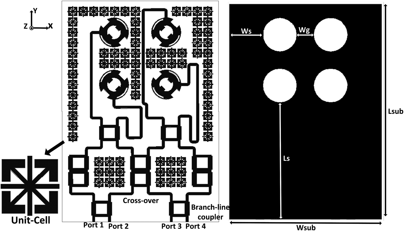
In this communication a 2 × 2 low-cost CP switched beam antenna array fed by 4 × 4 quasi butler matrix is proposed (see Fig. 1). Presented array is comprises of CP slot elements, feed network and modified uni-planner compact electromagnetic band-gap structure (UCEBG). The antenna element has circular polarization attribute that cause to improve the antenna 3 dB axial-ratio bandwidth. Moreover, sequentially rotated feed and periodic EBG structures are used, which leads to enhance circular polarization purity, impedance bandwidth, and radiation characteristics. UCEBG schemes are also utilized on corners of substrate, in feeding network and between the radiating elements to decrease mutual coupling and avoid unwanted excitation modes. Measured results illustrate that the fabricated antenna has impedance bandwidth of 2.9 GHz that extends between 4.1 and 7 GHz, and 3 dB axial-ratio bandwidth of 1.95 GHz between 4.6 and 6.55 GHz. Antenna gain is more than 9 dBi between 5 and 6 GHz.

Fig. 1. Configuration of presented Antenna array.
A) Antenna configuration
1) ELEMENT DESIGN
The modified geometry of single-fed proposed element with CP property is shown in Fig. 2. The procedure of element design is as followed:
-
Step (1) Create a circular ring patch with inner radius of R 1 and outer radius of R 2.
-
Step (2) Cut out two notches with width of W 2 and a length of L 2 along the outer periphery of ring patch at diagonal opposite points.
-
Step (3) Attach two stubs with dimensions of W 3 and L 3 at the inner periphery of ring patch with 90° rotated respect to notches.
-
Step (4) Insert a pair of arc-shaped slots on the ring patch.

Fig. 2. Geometry of array element with impedance and axial-ratio bandwidths.
The resonant frequency of element and CP property are mainly determined by the size and position of notches and attached stubs. Moreover impedance matching can be enhanced, by cutting circular slot with radius R 3 from ground plane. The arc-shaped slots change current distribution on the patch and lead to enhance CP characteristic. The single feed line is located at angle of 45° from notch and stub axis. This feed method excites two equally amplitude and orthogonal modes with 90° phase difference. Simulated frequency responses of impedance and axial-ratio bandwidths are evaluated by HFSS Ver. 15 and they are shown in Fig. 2. The total size of element is 22 × 28 × 0.8 mm3 which has been printed on FR4 dielectric substrate with relative permittivity of 4.4 and loss tangent of 0.024. Element dimensions are as follows (units: mm): L 1 = 5.5, L 2 = 5, L 3 = 3, L 4 = 28, W 1 = 1.5, W 2 = 2.12, W 3 = 1.2, W 4 = 0.85, W 5 = 22, R1 = 4, R 2 = 8.5, R 3 = 10, θ = 68°.
2) FEED NETWORK
Feeding network of presented beam-steering array is consists of four inputs, four outputs, two pairs of branch-line couplers, one crossover, two half crossovers, and 50 Ω microstrip lines, as shown in Fig. 3. Crossover is applied to isolate cross lines in the planner layout. The configuration of feed network is designed in a way that the mutual coupling was minimal. This geometry can help to enhance the accuracy of beam-steering in operational band. Two half-crossover are employed that helps to obtain signals with approximately equal amplitudes at feeding points of radiating elements. The distance between two adjacent radiating patches is 0.5 λ at 5.5 GHz, which λ is free space wavelength. For improving CP property, radiating elements are rotated 90° in clock wise direction. Desired phase difference among elements obtained by microstrip lines with appropriate lengths and a pairs of branch line couplers. Design and optimization procedure of proposed feed network is evaluated by Agilent advanced design system (ADS) commercial software. The curves of transmission and reflection coefficients for two ports (Port 1 and Port 2) excitation and differential phase diagram between ports are plotted in Fig. 3. The curves show agreeable performance of feed network in operational frequency range. The whole size of antenna array is 90 × 127 × 0.8 mm3, and fabricated on commercially cheap FR4-epoxy substrate. Additional dimensions of antenna are (units: mm): L sub = 127, L s = 67, W sub = 90, W s = 20, W g = 10.

Fig. 3. Simulated results of feeding network (a) transmission and reflection coefficients when port 1 is fed, (b) transmission and reflection coefficients when port 2 is fed, and (c) differential phase diagram between ports.
3) ELECTROMAGNETIC BAND-GAP STRUCTURE
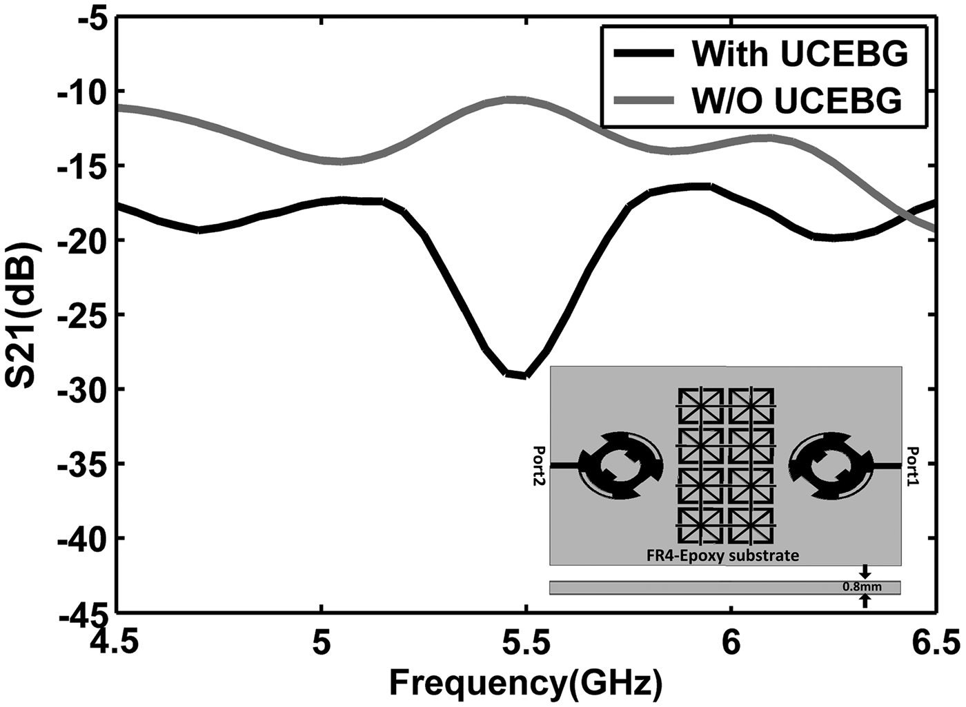
Microstrip patch antennas are usually used in arrays for achieving high gain and beam-steering property. The existence of the surface waves and overlapping near fields of radiating elements causes to intense mutual coupling, which significantly degrades the antenna's performance. Recently, various schemes of EBG structures have been investigated in antennas and microwave components. Due to the periodic nature of these structures, their physical size regulation are usually difficult, hence realizing EBG structure with compact size is important [Reference Chuang20]. Mushroom-like model is one of the first types and it is consisted of small metal pads with grounding vias. Although this specimen is sufficient scheme but requires a non-planar fabrication process [Reference Xu, Zhao, Lv, Du and Luo21]. Uni-planar compact EBG (UCEBG) structures composed of square metallic pads connected by strips mounted on grounded dielectric slab to form a LC network. They have small size and are interesting due to their easy fabrication. Conventional UCEBG structure consists of square pads and narrow lines with insets. The gap between the two adjacent cells presents equivalent capacitance and the strips together with insets demonstrate equivalent inductance [Reference Chang, Qian and Itoh22]. To obtain more compact scheme, the equivalent capacitance and inductance should be increased. In presented geometry insets are etched into the center part of the pad and only several conductor lines are remained, therefore the space over the center part has been used efficiently. Additional inductances are produced in this design, which are related with the extra magnetic flux flowing around the conductor lines. To verify the attributes of EBG structures and determining the band-gap regions, a 2 × 4 array of EBG structures are placed between the two 50 Ω open-ended microstrip-line (see Fig. 4(b)). One of the microstrip lines is used to excite the surface wave and another is resembled as the detector of the electromagnetic field intensity [Reference Xu, Zhao, Lv, Du and Luo21]. The EBG structures are utilized on FR4-Epoxy substrate whose permittivity is 4.4 and thickness is 0.8 mm. The simulated result for transmission coefficient is shown in Fig. 4(c). Due to the existence of EBG structures between two microstrip lines, the magnitude of S 21 significantly reduced at two ranges of 5.15–6.1 and 6.6–7.1 GHz. It means that propagation of surface wave is greatly repressed.

Fig. 4. (a) Geometry of EBG unit cell, (b) array of EBG structure, and (c) simulated result for transmission coefficient.
The extracted transmission coefficient curve between antenna elements with and without UCEBG is shown in Fig. 5. It is obvious that the mutual coupling among radiating elements is effectively decreases in presence UCEBG structure.

Fig. 5. Simulated transmission coefficient curve between antenna elements with and without UCEBG structure.
The EBG unit-cell dimensions in Fig. 4(a) are (units: mm): a = 6, b = 2, c = 0.75, d = 0.5, g = 0.25.
II. MEASURED RESULTS
The proposed beam-steering array was fabricated and measured to evaluate the design. The process of measurements is carried out for two antennas; (Ant. I: array without UCEBG and Ant. II: array equipped with UCEBG). The return-loss coefficients are measured by Agilent vector network analyzer 8722ES. Due to approximately symmetrical structure of array only ports 1 and 2 were excited in both antennas. The measured and simulated return-loss curves are depicted in Figs 6 and 7. Figure 6 exhibits the impedance bandwidths of both antennas when port 1 is excited. The measured impedance matching bandwidths are from 4.8 to 6.8 GHz (Ant. I) and 4.1 to 7 GHz (Ant. II). Figure 7 illustrates the impedance bandwidths for antennas, when port 2 is excited. The impedance bandwidths are covered from 4.65 to 6.6 GHz (Ant. I) and 4.25 to 6.75 GHz (Ant. II). It is understood from both figures, EBG structure causes approximately 20% bandwidth improvement.

Fig. 6. Simulated and measured results of return-loss for antennas when port 1 is fed.

Fig. 7. Simulated and measured results of return-loss for antennas when port 2 is fed.
The axial-ratio curves for antennas are shown in Figs 8 and 9. The measured axial-ratio bandwidth is from 4.6 to 6.55 GHz for port 1 and 4.7 to 6.7 GHz for port 2. It is interesting to note that, CP property is obtained in 66% of operating frequency range.

Fig. 8. Simulated and measured results of axial-ratio for port 1 excitation.

Fig. 9. Simulated and measured results of axial-ratio for port 2 excitation.
Extracted patterns at 5.5 GHz are plotted in Figs 10 and 11.

Fig. 10. Extracted far field results of RHCP and LHCP at 5.5 GHz when port 1 is fed.

Fig. 11. Extracted far field results of RHCP and LHCP at 5.5 GHz when port 2 is fed.
It can be found that the main beam directions are at θ = −18° for port 1 fed and θ = 20° for port 2 fed. Figure 12 shows the obtained results for axial-ratio as a function of elevation angel (θ) for both antennas at 5.5 GHz for two ports. The main lobe has circular polarization for −50° ≤ θ ≤ −15° and 10° ≤ θ ≤ 35° for ports 1 and 2 excitation, respectively. This figure shows that UCEBG structure, can partly improve the beam polarization.

Fig. 12. Obtained axial-ratio as function of elevation angle when two ports are excited.
Figure 13 shows the measured gain of both antenna arrays. The maximum values of gain are 8.2 dBi (Ant. I) and 11.2 dBi (Ant. II). It is better to mention that EBG structure has increased the peak gain of antenna with an average of ~2.5 dBi. Use of UCEBG structures helps to decrease surface waves produced by the antenna substrate. This phenomenon leads to concentrate current flow in patches and optimizes the radiation. In addition UCEBG structure resonates at operating frequency of array and causes to reduce the back radiation and increase overall efficiency.

Fig. 13. Measured gains for both antennas as versus of frequency for two ports excitation.
III. CONCLUSION
Beam-steering antenna array with improved impedance bandwidth, circular polarization purity, and radiation characteristics is proposed. Using the appropriate rotation technique, impedance, and axial-ratio bandwidths are effectively enhanced. EBG structures are utilized in the design of array to reduce the surface wave malicious effects and the mutual coupling between elements. It is note that, using EBG structure improves the overall operation of antenna. Four beams firing at different directions are obtained by exciting each port of network. The beams have good axial-ratio, agreeable gain, and CP diversity in their main lobes. The antenna array has impedance bandwidth over a frequency range of 4.1–7 GHz (~53%) for S 11 ≤ −10 dB and 3 dB axial-ratio bandwidth of 1.95 GHz that extends between 4.6 and 6.55 GHz (~35%). Measured maximum gain is 11 dBi at 5.5 GHz. Proposed array with its specific feed network is remarkable choice for smart wireless communications.
ACKNOWLEDGEMENT
The authors would like to acknowledge the help of electrical committee of science and research branch Islamic Azad University.
 Tohid Aribi was born in Urmia, Iran, in 1984. He received his B.Sc. degree in Telecommunication Engineering from IAU University, Urmia, Iran in 2005, and M.Sc. degree from IAU, South Tehran branch, Iran in 2009. Since 2010, he is in IAU University working with Telecommunications Department at faculty of Electrical and Computer Engineering. He is Ph.D. student in Telecommunication Engineering in SRBIAU University since 2011. He current interests are numerical techniques in electromagnetic, antenna, propagation, metamaterial and electromagnetic band gap (EBG) structure, substrate integrated waveguide (SIW), and array antenna.
 Mohammad Naser-Moghadasi was born in Saveh, Iran, in 1959. He received his B.Sc. degree in Communication Eng. in 1985 from the Leeds Metropolitan University (formerly Leeds polytechnic), UK. Between 1985 and 1987 he worked as an RF design engineer for the Gigatech company in Newcastle Upon Tyne, UK. From 1987 to 1989, he was awarded a full scholarship by the Leeds educational authority to pursue an M.Phil. for studying in CAD of Microwave circuits. He received his Ph.D. in 1993, from the University of Bradford, UK. Then he was offered a 2 years Post Doc. to pursue research on Microwave cooking of materials at the University of Nottingham, UK. From 1995, Dr. Naser-Moghadasi joined Islamic Azad University, Science and Research Branch, Iran, where he currently is an Associate Professor and head of postgraduate studies. His main areas of interest in research are Microstrip antenna, Microwave passive, and active circuits, RF MEMS. Dr. Naser-Moghadasi is member of the Institution of Engineering and Technology, MIET and the Institute of Electronics, Information and Communication Engineers (IEICE). He has so far published over 140 papers in different journals and conferences.
 R. A. Sadeghzadeh received his B.Sc. degree in Telecommunication Engineering from K. N. Toosi University of Technology, Tehran, Iran, in 1984, M.Sc. in digital communication engineering from the University of Bradford, Bradford, UK and the University of Manchester Institute of Science and Technology (UMIST), Manchester, UK, as a joint program in 1987, and the Ph.D. degree in Electromagnetic and antenna from the University of Bradford in 1991. During 1992 to 1997, he worked as a Postdoctoral Research Assistant in the field of propagation, electromagnetic, antenna, biomedical, and wireless communication with the University of Bradford. From 1984 to 1985, he was with Iran Telecommunication Company, Tehran, Iran, working on networking. Since 1997, he has been with the Faculty of Electrical and Computer Engineering, K. N. Toosi University of Technology. He has published more than 120 referable papers in international journals and conferences. His research interests include numerical techniques in electromagnetics, antenna, propagation, radio networks, wireless communications, nano antennas, and radar systems.