


I. INTRODUCTION
Cognitive radio (CR) is known as an efficient solution to reduce the spectrum scarcity, which is especially due to the lack of available frequency bands, which are already allocated by the Federal Communications Commission (FCC), to meet the strong demand of higher communication data rate and the significant number of wireless users [Reference Mitola and Maguire1]. CR is an intelligent wireless system, based on the concept of Software Defined Radio (SDR), which allows by several factors in the external and internal radio environment, such as network state, radio frequency spectrum, and user behavior, to provide the ability to adjust its parameters and adapt itself to optimize its operations [2]. This system is able to continuously supervise spectrum holes (white spectrum), and then dynamically tune its characteristics to operate within these unused frequency bands.
From the hardware point of view, the structures used in such a system must be reconfigurable to meet its requirements. The reconfigurability can be defined as the dynamic modification of one or several fundamental properties of the used components (i.e. antenna, filter, duplexer, and other devices). Recently, reconfigurable filters have been attracting much attention in CR applications due to their capability to dynamically adapt to the variability of the environment and to avoid the interference caused by the increasingly crowded spectrum. Filter reconfiguration techniques can be divided into two categories, continuous tuning and discrete tuning. The first technique can be obtained by using varactor diodes [Reference Hunter and Rhodes3, Reference Sanchez-Renedo, Gomez-Garcia, Alonso and Briso-Rodriguez4], micro-electrical mechanical systems (MEMS) capacitors [Reference Abbaspour-Tamijani, Dussopt and Rebeiz5, Reference Kim6], ferroelectric materials [Reference Courreges, Li, Zhao, Choi, Hunt and Papapolymerou7, Reference Subramanyam, Van and Miranda8], or ferromagnetic materials [Reference Murakami, Ohgihara and Okamoto9, Reference Tsai, Su and Lee10]. On the other hand, the discrete tuning technique can be generally achieved by employing either PIN diodes [Reference Koochakzadeh and Abbaspour-Tamijani11–Reference Karim, Guo, Chen and Ong14] or MEMS switches [Reference Ocera, Farinelli, Mezzanotte, Sorrentino, Margesin and Giacomozzi15, Reference Entesari, Obeidat, Brown and Rebeiz16]. Furthermore, several filter designs combining continuous and discrete tuning have been also investigated in the literature [Reference Yan and Mansour17]. However, most of the cited designs present a tunable center frequency or a reconfigurable response at the same frequency. For example, the authors in [Reference Karim, Guo, Chen and Ong14] present a ultra-wideband (UWB) bandpass-to-bandstop reconfigurable filter, but only at one resonant frequency.
Despite the extensive research on the reconfigurable filters, filters that can be reconfigured from bandpass to bandstop and switched between two different frequencies are very rarely reported. This paper presents a novel reconfigurable and switchable filter using two open-circuited stubs, which can be reconfigured from bandpass to bandstop filter and switched from 2.4 to 5 GHz. The discrete tunability of the proposed filter is achieved using two PIN diodes inserted at the end of each stub. The most distinguishing features of the proposed filter are its wide bandwidth with operation in the two most commonly used frequency bands (2.4 and 5 GHz), the switching between bandstop and bandpass response at both frequencies, and the low-cost fabrication due to use of the commercially available FR4 substrate and only two diodes. For the demonstration, a prototype of the proposed filter with total size of 55 × 60 mm2 (including feed lines, sub-miniature version A (SMA) connectors, and the bias circuit) has been designed, fabricated, and tested to verify the proposed concept. Measured results show a very good agreement with the simulated ones.
II. FILTER DESIGN AND ANALYSIS
A) Filter topology
In general, stopband or passband responses are accomplished by the creation of a zero-impedance or infinite-impedance to the transmission line at the desired frequency, respectively. In the present work, the passband response is achieved by introducing an infinite-impedance to the connecting transmission line, while the stopband response is obtained by creating a zero-impedance in the connecting line. To create the zero- or infinite-impedance to the transmission line, a quarter- or half-wavelength open-circuited stub is used, respectively. However, the number of the introduced stubs faces the dilemma of the good performance versus the encumbrance of stubs. Therefore, the need for the two-stub structure, rather than the one stub structure, is exigent, in order to ensure the best performance of the proposed filter in terms of return loss, increasing the rejection bandwidth by creating two transmission zeros on each side of the rejection band, and enhancing the bandwidth around the desired frequency.
As aforementioned, to switch from stopband to passband, the open-circuited stubs must be stretched by two times, i.e. from λ g /4 to λ g /2, which produces two transmission zeros on each side of the bandpass [Reference Pozar18]. Due to space limitations, this technique is replaced by the proposed method, which consists of grounding the two stubs directly via two PIN diodes, in order to turn the section from open to short-circuit, as shown in Fig. 1.

Fig. 1. (a) Initial and (b) proposed configurations of the proposed bandpass filter.
The final proposed structure consists of two quarter wavelength shunt stubs, calculated at the operating frequency 2.4 GHz, and separated from each by a distance of λ g /2 to provide a good isolation between them, as shown in Fig. 2. The transmission line connecting the two stubs is meandered, due to the necessity of reducing the total size of the structure, inasmuch as the proposed structure is intended to be integrated with the feed network of antennas used in CR applications. The two stubs are connected to ground via two switches to turn the section from open to short circuit.

Fig. 2. Proposed topology.
B) DC bias network
As aforementioned, in order to shorten the two open-circuited stubs, two switches based on PIN diodes are used. In this work, a switch circuit based on Infineon BAR88-02V PIN diode is used for electronic switching. It is forward-biased with a voltage of 0.95 V and a current of 100 mA. The equivalent circuit model used in full wave simulation, as extracted from the datasheet [19], is shown in Fig. 3. The diode presents a forward resistance R s in ON state of 1.5 Ω and a parallel circuit with a resistance of 65 kΩ and a capacitor of about 0.4 pF in the reverse bias state. The chip package presents a series parasitic inductor L 1 of about 0.5 nH. The overall package size is about 1.2 × 0.5 mm2.
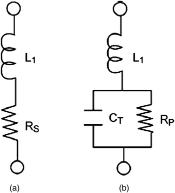
Fig. 3. Equivalent circuit model of the chosen PIN diode. (a) Forward bias. (b) Reverse bias.
As noted previously, both stubs must be open- or short-circuited simultaneously. To do this, the switches are biased with a single DC bias network. In order to properly bias the diodes, some design considerations must be taken into account, in terms of RF and DC signals isolation. The bias network used in this work consists of a high-impedance quarter-wavelength line, capacitors, and a radial stub. The aim of this network is to introduce an infinite-impedance at its input to prevent the RF signal from interfering with The DC source. Therefore, the quarter-wave line is used to transform a zero impedance to ideally infinite impedance. The zero impedance is established by of the radial stub due to its longer fringing capacitance at the open end. Furthermore, the zero impedance is enhanced by means of a 22 pF surface-mount-device (SMD) capacitor, as shown in Fig. 4. Moreover, the infinite-impedance is reinforced by the high-impedance of the transmission line. On the other hand, to prevent the DC signal from flowing into RF source and to maintain the RF continuity, two SMD capacitors of 22 pF are placed at the input and output of the filter. The PIN diodes are grounded through the use of two via-holes. The dimensions of the final topology are shown in Table 1.

Fig. 4. Final topology of the proposed reconfigurable and switchable filter.
Table 1. Dimensions of the proposed filter (in mm).

C) Equivalent circuit models
In order to explain how the proposed filter can operate in both modes (passband and stopband), an equivalent circuit model of the whole filter in the two states based on lumped elements is shown in Fig. 5. For simplicity, the connecting transmission line is modeled as a series combination of an inductor L 3 and a capacitor C 3. The open-circuited stub is modeled as a series LC resonant circuit (L 6 and C 6), while the short-circuited stub is modeled as an inductor L 2 in parallel with a capacitor C 2. Moreover, to properly model the proposed filter, the bias network is modeled as well. The high-impedance line is modeled as an inductor L 4 in series with a capacitor C 4, while the radial-line stub can be approximated as a series LC resonant circuit, consisting of a capacitor C 5 and an inductor L 5, connected in parallel with the grounded capacitor C s = 22 pF. Using Agilent ADS software [20], the performance of both circuits is simulated and shown in Fig. 6. As it can be seen, the modeled circuit in ON state presents a passband response around 2.4 GHz, while in the OFF state, the circuit provides a stopband response at the same frequency. Table 2 summarizes the filter responses for each diodes state.

Fig. 5. Lumped element equivalent circuit model of the proposed reconfigurable filter. (a) ON state. (b) OFF state.

Fig. 6. Simulated return losses of the modeled filter in ON state (solid-line) and in OFF state (dashed-line).
Table 2. Filter responses versus diodes biasing.

The equivalent circuit in Fig. 7 is a third-order filter composed of one element section 2 × θ 1 = λ g /2 wavelength with characteristic impedance Z A and two stubs of θ 3 = λ g /4 wavelength and characteristic impedance Z C . The DC biasing network consisting of a high-impedance quarter-wave and radial-line stubs is modeled as a transmission line of characteristic impedance Z B and wavelength θ 2 = λ g /4 + λ/8. The terms M A , M B , and M C represent the transmission matrices of Z A , Z B , and Z C , respectively:
 $$M_A = \left[ {\matrix{ {\cos \theta _1} & {jZ_A \cos \theta _1} \cr {j\displaystyle{{\sin \theta _1} \over {Z_A}}} & {\cos \theta _1} \cr}} \right],$$
 $$M_B = \left[ {\matrix{ 1 & 0 \cr {j\displaystyle{{\tan \theta _2} \over {Z_B}}} & 1 \cr}} \right],$$
 $$M_C = \left[ {\matrix{ 1 & 0 \cr {Z_e} & 1 \cr}} \right],$$
where Z e is the impedance of the stub, when the didoes are reverse-biased:
 $$Z_e = - jZ_C \cot \theta _3 $$
and when the diodes are forward-biased:
 $$Z_e = jZ_C \tan \theta _3. $$

Fig. 7. Equivalent transmission line model of the proposed filter.
Therefore, the overall ABCD matrix of the proposed filter can be obtained by multiplication of the sub-sections in sequence as follows:
 $$M_0 = M_A \times M_B \times M_A = \left[ {\matrix{ {A_0} & {B_0} \cr {C_0} & {D_0} \cr}} \right],$$
 $$M_1 = M_C \times M_0 \times M_C = \left[ {\matrix{ {A_1} & {B_1} \cr {C_1} & {D_1} \cr}} \right],$$
with
 $$A_1 = \mathop {\cos} \nolimits^2 \theta _1 \left( {1 - \displaystyle{{Z_A} \over {Z_B}} \tan \theta _2 - \tan \theta _1 + j2Z_A Z_e - \displaystyle{{Z_e Z_A^2} \over {Z_B}} \tan \theta _2} \right)$$
 $$B_1 = \mathop {\cos} \nolimits^2 \theta _1 \left( {jZ_A - \displaystyle{{Z_A^2} \over {Z_B}} \tan \theta _2 + jZ_A} \right),$$
 $$C_1 = \mathop {\cos }\nolimits^2 \theta _1\left[ \matrix{\tan \theta _2\left( {j\displaystyle{1 \over {Z_B}} - 2\displaystyle{{Z_eZ_A} \over {Z_B}} - \displaystyle{{Z_e^2 Z_A^2 } \over {Z_B}}} \right) + \hfill \cr \tan \theta _1\left( {j\displaystyle{2 \over {Z_A}} - 2Z_e} \right) + 2Z_e + j2Z_AZ_e^2 \hfill} \right], $$
 $$D_1 = \mathop {\cos} \nolimits^2 \theta _1 \left( {1 - \displaystyle{{Z_A} \over {Z_B}} \tan \theta _2 - \tan \theta _1 + j2Z_A Z_e - \displaystyle{{Z_e Z_A^2} \over {Z_B}} \tan \theta _2} \right).$$
Hence, using the ABCD to scattering (S) parameters transformation, the required S 11 and S 21 can be written as:
 $$S_{11} = \displaystyle{{A_1 + (B_1 /Z_0 ) + C_1 Z_0 - D_1} \over {A_1 + (B_1 /Z_0 ) + C_1 Z_0 + D_1}}, $$
 $$S_{21} = \displaystyle{{2Z_0} \over {A_1 + (B_1 /Z_0 ) + C_1 Z_0 + D_1}}. $$
The obtained equations are quite useful for determining the transmission and rejection bandwidths of the proposed filter. The derived equation (13) shows that the rejection bandwidth is strongly dependent on the connecting stub length (θ 1). In addition, since Z B , which represents the sum of the biasing line impedance and the radial stub impedance, is very high, M B becomes a unitary matrix (equation (2)), which its multiplication does not change the result. This can also be confirmed by equations (8)–(11). Therefore, this simply implies that the DC-biasing network has nearly no effect on the transmission or rejection bandwidths.
In summary, the design procedures of the proposed filter can be described as follows:
-
(1) The design procedure starts with a three-order bandstop filter;
-
(2) Transform the proposed filter from bandstop to bandpass, by shorting the stubs;
-
(3) Introduce two switches to ensure the transformation;
-
(4) Properly design the switches biasing network to not affect the filter performance;
-
(5) Modeling the proposed filter to evaluate the impact of each part of the circuit on the filter characteristics and to tailor the filter performance by using transmission line model;
-
(6) Finally, the proposed filter is fabricated and tested to verify the design concept.
III. SIMULATION AND EXPERIMENTAL RESULTS
After analyzing and designing the reconfigurable filter and its biasing network using Agilent ADS, a prototype is fabricated using LPKF milling machine to validate the circuit concept. The filter is manufactured on an FR4 substrate with a relative permittivity of 4.3 and a thickness of 1.58 mm. Excluding the feed lines, the overall filter dimensions are approximately 0.41λ g × 0.76λ g , where λ g is the guided waveguide at the center frequency 2.4 GHz. A photograph of the fabricated reconfigurable filter is shown in Fig. 8. The S-parameters were measured using an Anritsu MS2028C vector network analyzer (VNA) while a GW Instek AFG-2112 DC power supply was used to bias the diodes. The simulations were carried out by means of CST Microwave Studio and Ansoft HFSS software.

Fig. 8. Photograph of the fabricated filter.
Comparisons between the measured and simulated results of return losses and insertion losses are shown in Figs 9 and 10, respectively, for both states. From state ON to state OFF, the filter center frequency shifts from 2.6 to 5.57 GHz, which is corresponding to a frequency tuning ratio of 2.15:1. The 10 dB passband bandwidth is 100.76 and 45.78% for state ON and state OFF, respectively. The 10-dB bandwidth was chosen over the 3 dB bandwidth owing to the nature of the use of the proposed filter in antenna feed systems. Although, the 20 dB rejection bandwidth is 14.5 and 20.5% for state ON and state OFF, respectively. It is evident from the results that, despite a small discrepancy, a very good agreement is achieved between the measured and simulated results. The discrepancy between the results can be mainly attributed to the: (1) inaccuracies in the fabrication and measurement processes, (2) lack of proper modeling of diodes and capacitors, (3) effects of the feeding and RF cables in measurement, (4) parasatic of PIN diodes and capacitor, and (5) soldering imperfection in filter fabrication. Table 3 summarizes the performance of the proposed reconfigurable and switchable filter for both diodes states.

Fig. 9. Return loss of the proposed filter in ON state (a) and OFF state (b).

Fig. 10. Insertion loss versus frequency for the two switching cases, (a) switch ON and (b) switch OFF.
Table 3. The proposed reconfigurable and switchable filter performance.

Since the proposed filter includes active components and likewise the DC current that flows into the structure, the signal transmitted through the filter may be distorted. The phase characteristics of the filter are important to evaluate, in order to estimate its transmission distortion. To do this, the group delay (GD), which is the differential of the phase response, is calculated and shown in Fig. 11. The GD of this filter can be calculated by the following equation:
 $$\tau = \displaystyle{{\partial \angle S_{21}} \over {\partial \omega}}, $$
where
 $\angle S_{21} $
is the insertion loss phase and ω is the angular frequency in radians per second.
$\angle S_{21} $
is the insertion loss phase and ω is the angular frequency in radians per second.

Fig. 11. Measured GD of the proposed filter in ON state (solid line) and OFF state (dashed line).
Figure 11 shows the measured GD of the proposed filter for both diodes states. As can be observed, within the passband of each state, the measured GD is flat and below 1 ns with a variation of about 0.45 ns. The GD flatness and its small variation within the operational bandwidth in both states indicate that the proposed filter has good linear transmission characteristics and could not distort the transmitted signal.
The performance of the manufactured filter compared with those reported in other works are summarized in Table 4. As it can be noticed, the filter designs that provide both frequency and bandwidth tunability and reconfigurability are rarely reported. However, the proposed filter exhibits a good fractional bandwidth and a very wide tuning range of 2.4–5 GHz. Moreover, it can switch between bandpass to bandstop response at two frequencies. The proposed filter is designed on a low-cost FR4 substrate compared with other costly substrates used in reported designs. In addition, the proposed design incorporates only two PIN diodes, thus making the design simple and cheap to manufacture. To date, a simple miniature reconfigurable (bandpass-to-bandstop) as well as switchable filter from 2.4 to 5 GHz using only two PIN diodes has not been yet reported.
Table 4. Comparison of the proposed filter with reported reconfigurable filters.

IV. CONCLUSION
In this work, a simple reconfigurable and switchable filter has been presented using only two PIN diodes for CR front-ends. By controlling the bias voltage of both diodes simultaneously, the manufactured filter can be reconfigured from bandpass to bandstop and switched from 2.4 to 5 GHz. The proposed filter has been fabricated and tested results show a good agreement with the simulated ones. Moreover, the filter exhibits a flat GD in the passband of about 0.8–0.45 ns for both diodes states. The obtained results indicate that the fabricated reconfigurable filter is promising for CR front ends, and systems operating at 802.11 b/g/n/s and WiMAX bands. Furthermore, the proposed filter may be an effective solution to solve the serious problem of interferences between users in cognitive networks or between devices operating at 2.4 and 5 GHz bands.
ACKNOWLEDGEMENTS
The authors are grateful to Departamento de Ingenieria de Comunicaciones (DICOM), University of Cantabria (UNICAN), Spain, for support with regard to simulation software and facilities.
 Hamza Nachouane received his M.Sc. degree in Telecommunications and Microwave Devices with the highest grades from the National School of Applied Sciences of Fez, Morocco, in 2012. He is currently pursuing the Ph.D. degree at INPT (Institut National des Postes et Télécommunications, Rabat, Morocco). His main research interests include microstrip antennas, design, and analysis of reconfigurable antennas for cognitive radio and UWB applications, RF circuit design, diversity antennas, electrically small antennas, multi-input–multi-output antennas, phased array antennas, active and passive microwave devices.
 Abdellah Najid has Master degrees in Networking and Communication Systems and Ph.D. thesis in Microwaves and Wireless Networking in 1997 from Institut National Polytechnique de Toulouse INPT, France. Abdellah NAJID was working as researcher Engineer at INRIA Labs from 1998 to 2000. His research fields are routing protocols, wireless networking, microwave, and antennas design. Actually, Abdellah NAJID is a full Professor at Institut National des Postes et Télécommunications in Rabat, Morocco.
 Abdelwahed Tribak was born in Larache, Morocco, in 1981. He received the M.Sc. degree in Physics from Abdelmalek Essaadi University, Tetouan, Morocco, in 2006. He received a Master degree in Communications Engineering in 2008, and the Ph.D. of Telecommunication in 2011, both from the University of Cantabria, Santander, Spain. He is currently an associate Professor of antennas and microwave at the National Institute of Posts and Telecommunications, Rabat, Morocco. His main area of research is microwave circuits and systems, antenna feed subsystems for satellite, and radio-astronomy applications.
 Fatima Riouch is a Professor at INPT (Institut National des Postes et Télécommunications, Rabat, Morocco) since 1986. She graduated from ENAC Toulouse France in 1983 and then prepared a Certificate of Preparation for Research in Electronics and Communications at EMI, Rabat. In 2013, she became a qualified professor to supervise research. She has held several positions of responsibility at the INPT (head of the logistics department, education department head, and division head of continuing education, and currently coordinator of the Telecom engineering option). Her research is centered on antennas and wave propagation in the mobile radio environment.


