


1. INTRODUCTION
Modern communication systems require the design and development of the differential-mode bandpass filters (BPFs) with good common-mode suppression, such kind of filters exhibit higher invulnerability to low crosstalk, low electromagnetic interference, and low environmental noise in contrast with that of single-ended systems. To meet the above-mentioned requirements of communication system, researchers have developed many differential-mode BPFs with common-mode suppression. The earlier developed differential-mode BPFs are available using single [Reference Shi and Xue1], multi-section [Reference Wu, Wang and Chen2], and half-wavelength resonators [Reference Shi and Xue3]. These BPFs have good common-mode rejection in the differential-mode passband with planar topologies. However, they have low-quality factor; some of them are electrically large in size and low-power handling capability [Reference Shi and Xue1–Reference Shi and Xue3]. After that, several improved performance balanced BPF have been designed and developed using coupled line structures [Reference Wu, Wang and Chen4], split ring resonator [Reference Tamura, Ishizaki and Hoft5], defected ground plane [Reference Liu, Tsai, Han and Wu6], transformer integrated using integrated passive device's technology [Reference Wu, Kuo and Chen7], dual-mode balanced BPF by utilizing strip line resonator [Reference Shi, Chen and Xue8], and also using stepped-impedance resonators [Reference Wu, Wang and Chen9]. Good differential-mode selectivity and significantly reduced size balanced BPF using low-temperature co-fired ceramic technology is also presented in [Reference Chen, Shao and Lu10]. Substrate-integrated waveguide-based differential-mode BPF can exhibit good common-mode rejection in the differential-mode passband, beside its compact size [Reference Chen, Hong and Ho11]. The quality factor and size are not optimum, but many of those filters are quite useful. Indeed planar implementations are preferred to dielectric resonator (DR) implementations in many applications. However, modern high-speed communication system requires filters having high Q, low losses, compact in size, good common-mode rejection, and superior in band response along with spurious free out-of-band response. DR mounted on a planar surface is one of the favorite choices for such applications. Recently, two differential-mode BPFs using DR have been reported [Reference Chen, Zhan, Qin, Bao and Xue12, Reference Zhan, Li, Qin and Chen13], which have good common-mode suppression in the differential-mode passband. One of them consists of two rectangular resonators mounted on the PCB substrate. A pair of microstrip feeding lines is used to excite TE11δ -mode in the differential-mode passband of the filter. The disadvantage of this design includes custom made DR and high insertion loss (IL) in the differential-mode passband of the filter. However, Zhan et al. [Reference Zhan, Li, Qin and Chen13] make use of a ring-type DR with probe excitation. Probe excitation makes this structure non-planar. In addition, another disadvantage of the above design is its low spurious performance.
This paper presents a synthesis and design method of common-mode suppressed differential BPF having ring dielectric resonator (RDR) excited by a pair of the microstrip line. In addition, the microstrip feed line is introduced transmission zeros (TZs) in the lower and upper stopband of the filter. Finally, a second-order differential-mode BPF is designed at a center frequency of 3.93 GHz with fractional bandwidth (FBW) of 1.5% and IL of 0.6 dB.
II. CHARACTERISTICS OF RDR
An RDR can resonate in various modes having different resonating frequencies. Figures 1 and 2 present the electromagnetic field distribution of the first two modes in RDR under differential mode, obtained using HFSS. According to the resemblance of their field distribution, the first mode is TE01δ -mode, while the second mode is TM01δ .

Fig. 1. Field distribution of TE01δ mode. (a) Electric field. (b) Magnetic field.

Fig. 2. Field distribution of TM01δ -mode. (a) Electric field. (b) Magnetic field.
First, keeping the inner radii and the height of the RDR constant, varying the outer radii from 2 to 3.8 mm, TM01δ -mode resonant frequency will decrease, while TE01δ -mode frequency is almost constant. As we increase the outer radii beyond 3.8 mm, the resonant frequency of the TM01δ -mode becomes almost constant, but the resonant frequency of the TE01δ -mode will be decreased, as shown in Fig. 3(a). Similarly, we observed that the variation in inner radii did not influence the resonant frequency of the TM01δ -mode, while the resonant frequency of the TE01δ -mode would be increased from 3.5 to 3.75 GHz, as illustrated in Fig. 3(b).
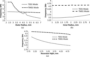
Fig. 3. Resonant frequencies of theTM01δ and TE01δ -mode with (a) outer radius, (b) inner radius, and (c) height of the resonator.
As shown in Fig. 3(c), the resonance frequency of the TM01δ - and TE01δ -mode are decreasing with the height of the RDR. It can be seen that the variation in outer radius and height will be affected the resonant frequency of the RDR. However, variation in the inner radius will have very small effect on the resonance frequency of the resonator. Q-factor is a measure of the loss of the DR, lower the losses associated with the DR higher the value of the quality factor (Q). However, the quality factor of the DR will be depend on the length of the microstrip feed line and the gap (g), as illustrated in Fig. 4. The quality factor of RDR coupled with a balanced transmission line is as follows:
 $$\displaystyle{1 \over {Q_u}} = \displaystyle{1 \over {Q_c}} + \displaystyle{1 \over {Q_d}} + \displaystyle{1 \over {Q_{leak}}}, $$
where Q c , Qd , and Q leak correspond to the conductor, dielectric, and leakage losses, respectively.

Fig. 4. Schematic of the proposed filter.
Q leak is considered to be zero. Figure 5 shows the relationship between the length of the microstrip feed line and quality factor for the different value of the gap (p), quality factor has been decreasing with the increase in the length of the microstrip feed line, after 7.5 mm the quality factor becomes constant around 300.

Fig. 5. Q factor of TE01δ -mode.
III. COUPLING CONTROL
The coupling coefficients can be computed by determining even-mode and odd-mode resonant frequencies f 1 and f 2 of the structure and by applying the equation (1)
 $$k = \displaystyle{{f_2^2 - f_1^2} \over {f_2^2 + f_1^2}}. $$
The amount of coupling depends on the distance between microstrip feed lines and resonator. Coupling between the resonators can be controlled by varying the distance between the DRs for different value of gap (g), as shown in Fig. 6. As illustrated in Fig. 6, in the case of common mode the coupling coefficient will be affected to a certain extent, but in the case of differential-mode coupling coefficient will be vary with the change of the distance between DRs.
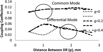
Fig. 6. Variation of coupling coefficient with distance between the DR for different value of the gap (g) between the DR and stub.
IV. REALIZATION OF TZ
A variation of the TZs frequencies with the distance between the DR for different value of the gap (g) between the DR and stub is presented in Fig. 7. A TE01δ -mode dielectric filter coupled with a pair of microstrip feed line will be create a TZ in the upper and lower stopband of the differential mode. From Fig. 7, it has been observed that the position of the TZs is changing with increasing the gap (g). Hence, TZs are only affected by the gap between DR and stub. Thus, in order to design a differential-mode filter with good selectivity, the position of the TZs, can be controlled by varying the gap between the feeding line and DR.

Fig. 7. Variation of TZs frequencies with distance between the DR for different value of the gap (g) between the DR and stub.
V. CIRCUIT REALIZATION OF SECOND-ORDER BPF
A second-order lowpass prototype network has been considered, as shown in Fig. 8(a). The element value of the filter in terms of “g” parameters are g 0 = 1, g 1 = 0.66482, and g 2 = 0.12665, where “g” may be a shunt capacitor or series inductor. Well-known, dual network theorem has been used to transform a series inductor to shunt capacitor. After transformation new circuit consists of all admittance or conductance, and is called a parallel resonance lowpass filter prototype circuit, as shown in Fig. 8(b). In a next step, this parallel resonance lowpass filter has been used to realize a BPF by replacing the admittances with a parallel L–C circuit and doing the appropriate scaling for the resonance frequency and bandwidth. The scaled BPF is shown in Fig. 8(c). Symmetric and anti-symmetric sources or even- and odd-mode analyses are used to obtain the general equation for inverter-coupled parallel resonance network.

Fig. 8. Lowpass to BPF transformation. (a) Lowpass prototype. (b) Lowpass prototype after application of dual network theorem. (c) Bandpass prototype network.
A) Even-mode analysis
The ABCD matrix could be obtained by using the even-mode analysis. Bisect the filter network has shown in Fig. 9 with open circuit along the symmetry plane (XX′). Then, looking into the two ports, the ABCD matrix of the network is given below:
 $$\left[ {\matrix{ { - 1} & 0 \cr { - 1} & 0 \cr}} \right]$$

Fig. 9. BPF in symmetric form.
B) Odd-mode analysis
For the odd-mode excitation, there is a voltage null along the middle of the filter network shown in Fig. 9. Thus, this filter network has been bisected along the symmetry plane (XX′). The symmetry plane behaved as an electric wall in the differential mode, hence they are grounded. Then, looking into the two ports, the ABCD matrix of the network is given below:
 $$\eqalign{&\left[\matrix{ - 1 - \left(j\omega 2C_{11} + \displaystyle{2 \over j\omega L_{11}} \right) \left(j\omega 2C_{22} + \displaystyle{2 \over j\omega L_{22}} \right) \cr - \left( j\omega 2C_{11} + \displaystyle{2 \over j\omega L_{11}} \right)}\right. \cr &\quad \left. \matrix{ - \left(j\omega 2C_{22} + \displaystyle{2 \over j\omega L_{22}} \right) \cr - 1} \right].}$$
The above-discussed ABCD matrix have been used to obtain the resultant S-parameter response of the realized BPF, as shown in Fig. 10. In the next section, we will realize this BPF with the help of RDR.

Fig. 10. Frequency response of the realized BPF.
VI. REALIZATION OFBPF USING RDR
To validate the proposed concept a second-order TE01δ -mode, differential-mode DR filter has been designed and implemented as shown in Fig. 11(a). Specification chosen for the design of the second-order differential-mode DR filter is as follows: center frequency 3.93 GHz, return loss (RL) 20 dB in the differential-mode passband, FBW 0.5%, and 0.5 dB passband ripple. To employed differential-mode filter, the RDR [14] has dielectric constant 98 and quality factor >1200. Two RDRs are placed on the RT-Duriod substrate having relative permittivity ε r = 2.2, height h = 30 mil feed with a pair of 50 Ω microstrip lines, located on both sides of the RDR. The 3D EM software HFSS has been used to design and simulate the proposed BPF. Figure 11(b) also shows the fabricated RDR based BPF, whose dimensions are given in the Table 1. A pair of microstrip line coupled with the RDR can excite TE01δ -mode in the differential-mode passband and TE01δ -mode in the common-mode passband of the filter. Since, both the modes have a different resonant frequency, so that good common-mode suppression can be achieved in the differential-mode passband of the DR filter. Input and output coupling have been used to introduce the TZs in the left- and right-hand sides of the center frequency. The introduction of the TZs has been used to improve the selectivity of the proposed BPF.

Fig. 11. Proposed differential-mode BPF. (a) Layout of the proposed BPF. (b) Fabricated BPF.
Table 1. Dimension of the filter.

Figure 12 shows, the simulated and measured S-parameter of the proposed differential-mode BPF. The measured diffferential mode passband centered at 3.93 GHz with 3-dB FBW of 1.5%. The simulated and measured S-parameters of the differential-mode BPF are in good agreements. From the broadband response of the filter, it can be observed that a TZs appear in the lower and upper stopband of the differential-mode filter and rejection level of more than 50 dB, which is achieved in the differential-mode passband of the filter. Comparisons with the previously reported balanced BPF are summarized in Table 2. The proposed BPF exhibits better performance.

Fig. 12. Simulated and measured frequency response of the proposed BPF.
Table 2. Performance comparison with previous work.

VII. CONCLUSION
This paper demonstrated synthesis, design, and analysis of second-order differential-mode BPF. The proposed differential-mode BPF has a planar configuration, high Q with simple coupling configuration and high common-mode rejection level (50 dB). TE01δ and TM01δ -mode are effectively excited in differential and common-mode configuration, respectively. TZs are also created in the lower and upper stopband of the filter to improve the selectivity of the differential-mode BPF. To validate the proposed concept a differential-mode BPF using the RDR has been fabricated and its frequency response is measured.
ACKNOWLEDGEMENT
The author would like to acknowledge the Department of ECE, Ambedkar Institute of Advanced Communication Technologies and Research, Geeta Colony, New Delhi-110031, India for providing technical assistance at each stage of this project.
 Jugul Kishor received his B.Tech. degree in Electronics Engineering from KNIT Suktanpur, India in 2002 and M.Tech. degree in microwave Electronics in 2008 from the University of Delhi, Delhi, India. Currently, he is working toward his Ph.D. degree in Electronics Engineering from Indian School of Mines, Dhanbad, India. His recent research interest activities have focused on the design and development of dielectric reonator filters and antennas. He is also a member of IEEE MTT-S.
 Binod Kumar Kanaujia is working as a Professor in the School of Computational and Integrative sciences, Jawaharlal Nehru University, New Delhi since August, 2016. Before joining Jawaharlal Nehru University, he had been in the Department of Electronics & Communication Engineering in Ambedkar Institute of Advanced Communication Technologies & Research (formerly Ambedkar Institute of Technology), Delhi as a Professor since February 2011 and Associate Professor (2008–2011). Dr. Kanaujia held the positions of Lecturer (1996–2005) and Reader (2005–2008) in the Department of Electronics & Communication Engineering, and also as the Head of the Department in the M.J.P. Rohilkhand University, Bareilly, India. Prior to his career in academics, Dr. Kanaujia had worked as an Executive Engineer in the R&D division of M/s UPTRON India Ltd. Dr. Kanaujia had completed his B.Tech. degree in Electronics Engineering from KNIT Sultanpur, India in 1994. He did his M.Tech. and Ph.D. in 1998 and 2004; respectively, from the Department of Electronics Engineering, Indian Institute of Technology Banaras Hindu University, Varanasi, India. He has been awarded Junior Research Fellowship by UGC Delhi in the year 2001–2002 for his outstanding work in electronics field. He has keen research interest in design and modeling of microstrip antenna, dielectric resonator antenna, left-handed Metamaterial microstrip antenna, shorted microstrip antenna, ultra wideband antennas, reconfigurable and circular polarized antenna for wireless communication. He has been credited to publish more than 150 research papers with more than 430 citations with h-index of 12 in peer-reviewed journals and conferences. He had supervised 50 M.Tech. and 08 Ph.D. research scholars in the field of microwave engineering. He is a reviewer of several journals of international repute, i.e. IET Microwaves, Antennas & Propagation, IEEE Antennas and Wireless Propagation Letters, Wireless Personal Communications, Journal of Electromagnetic Wave and Application, Indian Journal of Radio and Space Physics, IETE Technical Review, International Journal of Electronics, International Journal of Engineering Science,IEEE Transactions on Antennas and Propagation, AEU-International Journal of Electronics and Communication, International Journal of Microwave and Wireless Technologies, etc. Dr. Kanaujia had successfully executed four research projects sponsored by several agencies of Government of India, i.e. DRDO, DST, AICTE, and ISRO. He is also a member of several academic and professional bodies, i.e. IEEE, Institution of Engineers (India), Indian Society for Technical Education, and The Institute of Electronics and Telecommunication Engineers of India.
 Santanu Dwari was born in Howrah, West Bengal, India. He received his B.Tech. and M.Tech. degrees in Radio Physics and Electronics from the University of Calcutta, Kolkata, West Bengal, India in the year of 2000 and 2002 respectively and Ph.D. degree from Indian Institute of Technology, Kharagpur, West Bengal, India in the year of 2009. He joined Indian School of Mines, Dhanbad, Jharkhand, India in 2008 where he is currently an Assistant Professor in the Department of Electronics Engineering. He has published seven research papers in referred International Journals. He is carrying out two sponsored research project as Principal Investigator. His research interest includes Antennas, RF planar circuits, and Computational Electromagnetics.
 Ashwani Kumar received his B.Sc. (Hon.) Electronics, M.Sc. Electronics, M.Tech. Microwave Electronics, and Ph.D. degrees in 2000, 2004, 2006, and 2014, respectively from the University of Delhi, Delhi, India. Currently, he is an Assistant Professor at the Department of Electronics, Sri Aurobindo College, the University of Delhi, Delhi, India. His current research interests design and development of microwave passive components such as microstrip filters, dielectric resonator-based filters, and circularly polarized antennas using metamaterial. He is a Member of IEEE Microwave Theory and Techniques Society. He has published 45 journal and conference technical papers on filters and antennas.


