I. INTRODUCTION
Envelope tracking [Reference Kahn1] has shown itself to be an efficient method of amplifying contemporary communications standards with large peak-to-average power ratios (PAPR) such as long-term evolution (LTE) [2] by manipulating the supply voltage to radio frequency (RF) power amplifiers (PA) with a modulator in harmony with the transmitted RF signal. Ideally, this modulator consists of only a high bandwidth switched mode power supply (SMPS) [Reference Habler, Ellinger, Jorges, Wolf and Lindner3]. At low-switching frequencies (i.e. <1 MHz) SMPS efficiencies of 95% are possible, but efficiency rapidly decreases as the switching frequency increases to the tens or even hundreds of megahertz necessary for LTE. One proposal is to switch between multiple supply voltages at high speed [Reference Augeau, Bouysse, Martin, Nebus, Quéréa, Lapierrea, Jardela and Piotrowicz4], but this generates significant output noise and cannot achieve sufficient granularity to meet the stringent emission masks.
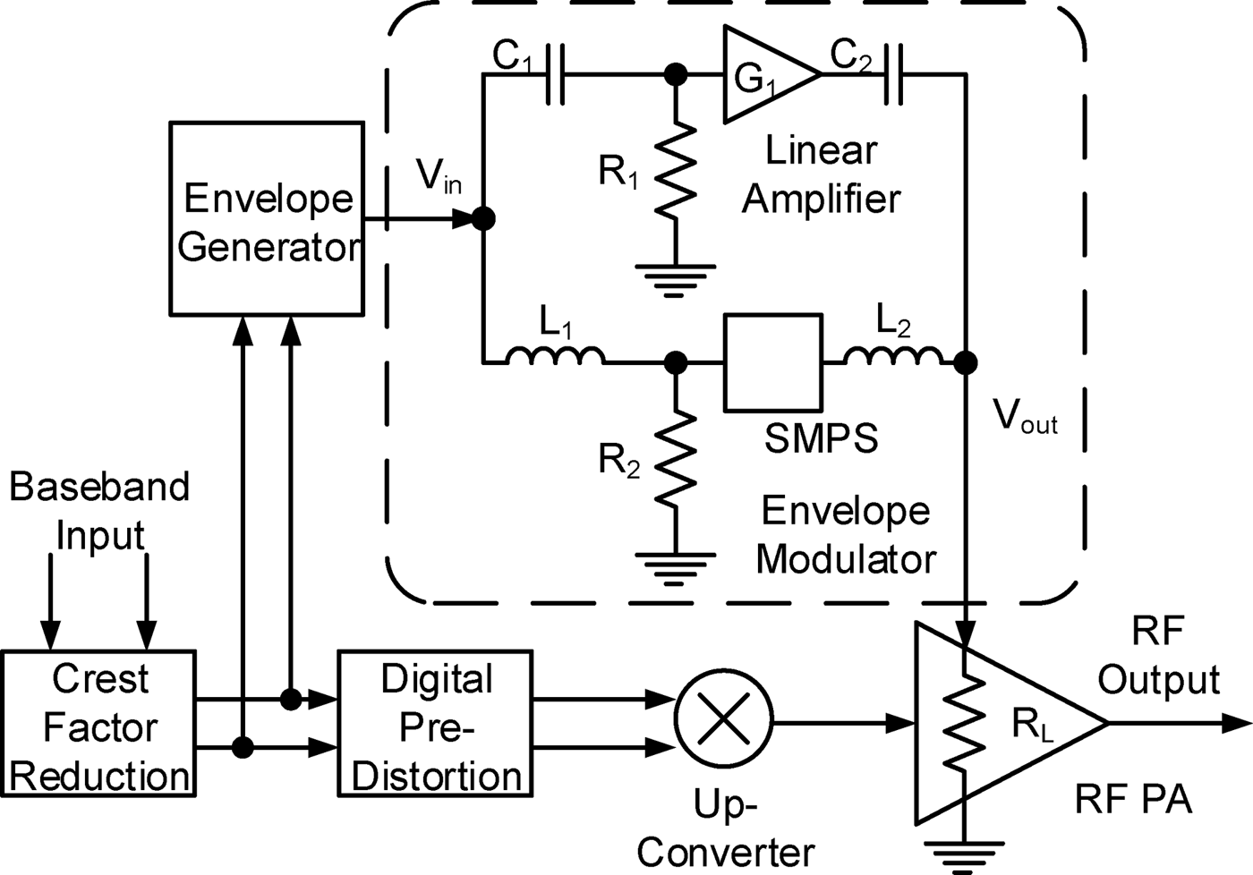
A more practical modulator design combines a high-efficiency low-switching frequency SMPS and a low-efficiency high bandwidth Linear Amplifier in a split frequency architecture [Reference Raab5]. A typical split frequency envelope tracking (ET) transmitter architecture is shown in Fig. 1 where the low-frequency component is low-pass filtered by L 1, R 2, and L 2, and amplified by an SMPS. The high-frequency content is filtered by C 1, R 1, and C 2, and amplified a Linear Amplifier (G 1). The resulting envelope signal is then applied to the supply voltage terminal of the RF PA which has an equivalent drain impedance of R L. In Fig. 1, crest factor reduction is used to reduce the high PAPR of the input baseband signal. From this the envelope signal is extracted and applied to the envelope modulator. Digital pre-distortion is used to improve system linearity.

Fig. 1. Split frequency envelope tracking RF PA; R L is the equivalent drain impedance of the RF PA.
Splitting and recombining the envelope signal into low- and high-frequency paths introduce a 360° phase transient at the crossover point due to the phase shift experienced by each path, and then when combined in anti-phase. When amplifying a modulated signal, this phase transient leads to distortion at the RF output which is hard to compensate for. Solutions proposed in the literature have used either impractical negative impedances for C 1 and L 1 [Reference Raab5] or complex filtering functions [Reference Yousefzadeh, Alarcon and Makismovic6]. In this paper, a simpler solution is proposed based on a lead-lag structure which can be implemented without excessive system overheads.
This paper is organized as follows: First the split frequency envelope modulator of Fig. 1 will be mathematically analyzed in Section II and the lead-lag modulator analyzed in Section III. Both modulators will be simulated in Section IV with an LTE signal to quantify the improvement. A modification to the lead-lag modulator using synthetic impedance, whose function is to maintain high system efficiency will be discussed in Section V. Implementation of a practical modulator will be discussed in Section VI. Results are presented in Section VII and the paper concluded in Section VIII.
II. SPLIT FREQUENCY ENVELOPE MODULATOR
To fully understand how the split frequency modulator operates it should be first analyzed mathematically. In its simplest form it consists of both a low-pass and a high-pass filter in parallel. As frequency increases the low-pass filter rolls-off and the high-pass filter starts to pass the signal, thus becomes the dominant path. Assuming in Fig. 1 that both G 1 and the SMPS have unity gain, the transfer function can be expressed as:
 $$\displaystyle{{{V_{out}}} \over {{V_{in}}}} = \displaystyle{{\displaystyle{{{R_1}{C_1}{C_2}{L_2}{s^3}} \over {1 + {R_1}{C_1}s}} + \displaystyle{1 \over {1 + ({L_1}/{R_2})s}}} \over {({L_2}/{R_L})s + {C_2}{L_2}{s^2} + 1}}.$$
In the ideal modulator all filters would have an equal cut-off frequency. Therefore all capacitors are equal to C, resistors equal to R, and inductors equal to L:
 $$\displaystyle{{{V_{out}}} \over {{V_{in}}}} = \displaystyle{{\displaystyle{{RL{C^2}{s^3}} \over {1 + RCs}} + \displaystyle{1 \over {1 + (L/R)s}}} \over {(L/R)s + CL{s^2} + 1}},$$
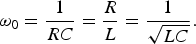 $${\omega _0} = \displaystyle{1 \over {RC}} = \displaystyle{R \over L} = \displaystyle{1 \over {\sqrt {LC}}}.$$
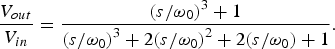 $$\displaystyle{{{V_{out}}} \over {{V_{in}}}} = \displaystyle{{{{(s/{\omega _0})}^3} + 1} \over {{{(s/{\omega _0})}^3} + 2{{(s/{\omega _0})}^2} + 2(s/{\omega _0}) + 1}}.$$
Making the substitution:
 $$s = j\omega,$$
we arrive at:
 $$\displaystyle{{{V_{out}}} \over {{V_{in}}}} = \displaystyle{{1 - j{{(\omega /{\omega _0})}^3}} \over {1 - j{{(\omega /{\omega _0})}^3} - 2{{(\omega /{\omega _0})}^2} + 2j(\omega /{\omega _0})}}.$$
At the crossover frequency when ω = ω 0:
 $$\displaystyle{{{V_{out}}} \over {{V_{in}}}} = \displaystyle{{1 - j} \over {j - 1}},$$
which results in unity gain at the crossover frequency, but with a phase of −180°.
III. LEAD-LAG ENVELOPE MODULATOR
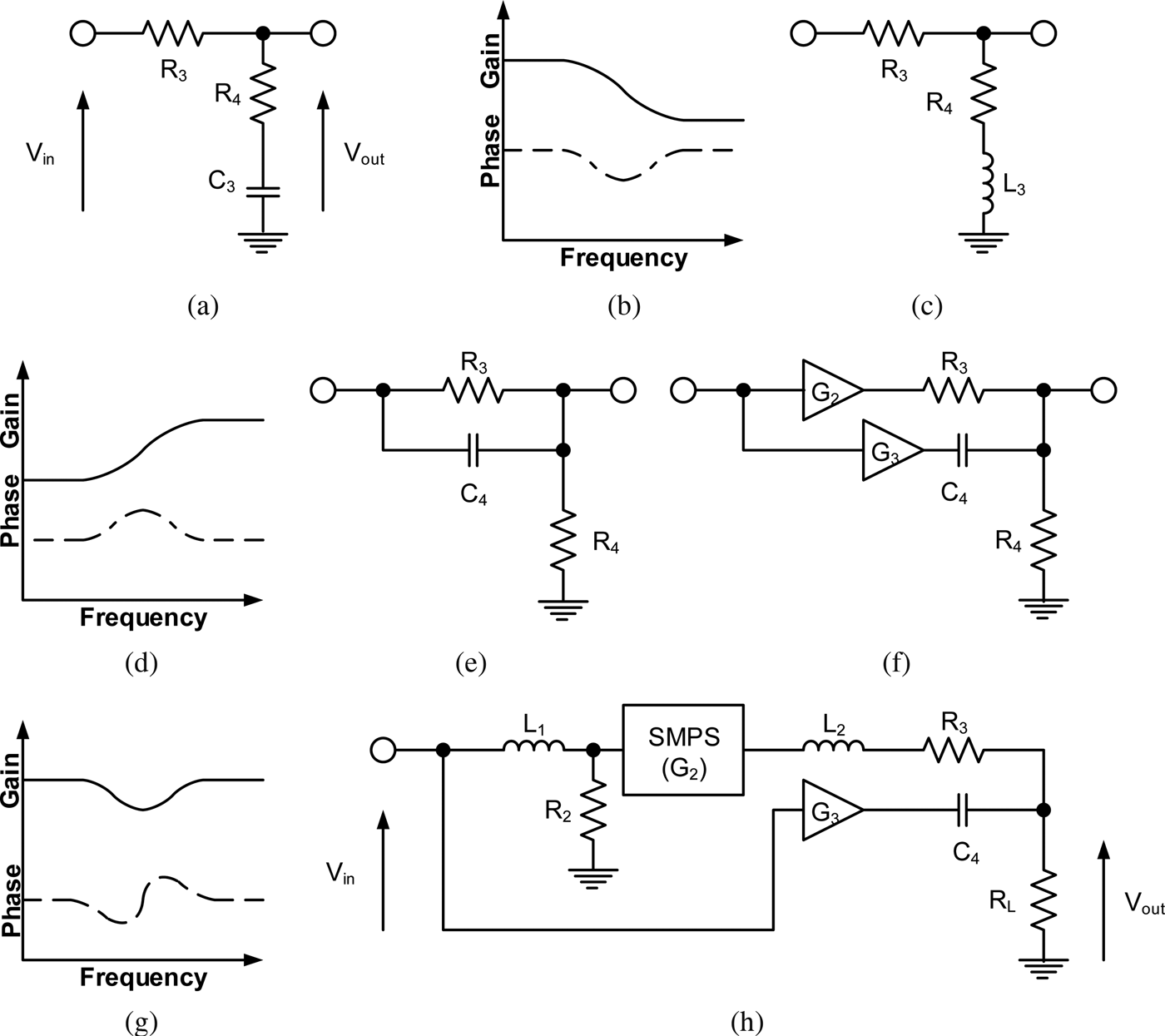
The new architecture proposed here is based on a lead-lag network. This is the dual of the lag-lead network often used in the feedback loop of phase-locked loops [Reference Egan7] and shown in Fig. 2(a). Its frequency response is shown in Fig. 2(b), where at low frequencies C 3 has a high impedance; so zero attenuation or phase shift is introduced. As frequency increases, the impedance of C 3 drops attenuating the output and introducing a phase shift. At high frequencies where C 3's impedance tends to zero, R 3 and R 4 form a potential divider with zero overall phase shift. The dual of the lag-lead network is the lead-lag shown in Fig. 2(c) which attenuates signals at low frequencies, but not at high ones. Its response is shown in Fig. 2(d), which also shows that there is zero phase shift at high and low frequencies.
Fig. 2. (a) Lag-lead network and its frequency response (b), (c) lead-lag network and its frequency response (d), (e) capacitor lead-lag network, (f) gain compensated lead-lag network and its frequency response (g), (h) lead-lag-based modulator.
The inductor L 3 can be replaced with a capacitor (C 4) as shown in Fig. 2(e) to achieve the same transfer function where high-frequency content bypass R 3 through C 4. Amplifiers (G 2 and G 3) can be introduced into Fig. 2(e) to form Fig. 2(f) and their gains selected, so that the low- and high-frequency gains are equal, as shown in Fig. 2(g). This introduces a phase transient, but one which is less severe than that of the original split frequency modulator. For simplification, it is assumed that R 3 is equal to R L, so the gains of G 2 and G 3 are such that:
 $${G_2} = 2{G_3}.$$
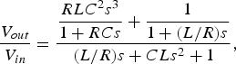
Finally, in Fig. 2(h) the low-frequency amplifier G 2 is replaced by an SMPS. This SMPS is band limited by its control loop and switching frequency. Past work has shown that the maximum bandwidth is in the order of 20 kHz for an off-the-shelf SMPS IC [Reference Watkins8]. The overall crossover frequency must be set lower than the SMPS bandwidth, so that it does not interfere. L 2 is selected to isolate the smoothing capacitor present at the SMPS's output at high frequencies. This is of no consequence, since the current flow through the high-frequency path (G 3 and C 4) will dominate in this region of the frequency domain. The cut-off of the input filter formed from L 1 and R 2 is set to the same frequency as L 2 and R 3. G 3 is equivalent to the Linear Amplifier in Figure 1 with R L takes the place of R 4. The transfer function of Fig. 2(h) can be derived as:
 $$\displaystyle{{{V_{out}}} \over {{V_{in}}}} = \displaystyle{{{R_L}{C_4}s + {L_2}{C_4}{s^2} + \displaystyle{2 \over {1 + ({L_1}/{R_2})s}}} \over {({L_2}/{R_L})s + {L_2}{C_4}{s^2} + {R_L}{C_4}s + 2}}.$$
By making all resistors equal to R, and inductors equal to L:
 $$\displaystyle{{{V_{out}}} \over {{V_{in}}}} = \displaystyle{{R{C_4}s + L{C_4}{s^2} + \displaystyle{2 \over {1 + (L/R)s}}} \over {(L/R)s + L{C_4}{s^2} + R{C_4}s + 2}}.$$
In the original split frequency modulator all filters had equal cut-off frequencies; this is not true for the lead-lag since the pass-bands must overlap:
 $${\omega _1} = (R/L),$$
 $${\omega _2} = (1/R{C_4}), $$
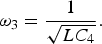 $${\omega _3} = \displaystyle{1 \over {\sqrt {L{C_4}}}}.$$
Substituting (11), (12), and (13) into (10):
 $$\displaystyle{{{V_{out}}} \over {{V_{in}}}} = \displaystyle{{(s/{\omega _2}) + {{(s/{\omega _3})}^2} + \displaystyle{2 \over {1 + (s/{\omega _1})}}} \over {(s/{\omega _1}) + {{(s/{\omega _3})}^2} + (s/{\omega _2}) + 2}}.$$
To ensure the pass-bands overlap, ω 1 is set to three times ω 2. A factor of 3 is a slightly arbitrary value chosen as a compromise because the SMPS path has a finite upper bandwidth. The lower cut-off frequency of the high-frequency band is reduced with C 4. ω 2 and ω 3 are scaled thus:
 $${\omega _2} = ({\omega _1}/3),$$
 $${\omega _3} = \displaystyle{{{\omega _1}} \over {\sqrt 3}}.$$
Substituting (15) and (16) into (14):
 $$\displaystyle{{{V_{out}}} \over {{V_{in}}}} = \displaystyle{{3(s/{\omega _1}) + 3{{(s/{\omega _1})}^2} + \displaystyle{2 \over {1 + (s/{\omega _1})}}} \over {(s/{\omega _1}) + 3{{(s/{\omega _1})}^2} + 3(s/{\omega _1}) + 2}}.$$
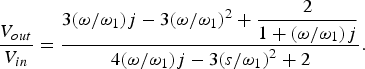 $$\displaystyle{{{V_{out}}} \over {{V_{in}}}} = \displaystyle{{3(\omega /{\omega _1})j - 3{{(\omega /{\omega _1})}^2} + \displaystyle{2 \over {1 + (\omega /{\omega _1})j}}} \over {4(\omega /{\omega _1})j - 3{{(s/{\omega _1})}^2} + 2}}.$$
Rearranging (18):
 $$\displaystyle{{{V_{out}}} \over {{V_{in}}}} = \displaystyle{{3{{(\omega /{\omega _1})}^3}j - 3(\omega /{\omega _1})j + 6{{(\omega /{\omega _1})}^2} - 2} \over {3{{(\omega /{\omega _1})}^3}j - 6(\omega /{\omega _1})j + 7{{(s/{\omega _1})}^2} - 2}}.$$
At the crossover frequency where ω = ω 1:
 $$\displaystyle{{{V_{out}}} \over {{V_{in}}}} = \displaystyle{4 \over {5 - 3j}},$$
Eq. (20) has a magnitude of 0.69 at the crossover frequency. This will result in a null of −3.3 dB in the gain response, with a phase shift of 30.9°. The phase shift causes a delay resulting in time misalignment between the two signal paths at the crossover frequency. That of the lead-lag modulator is significantly less than the −180° of the original modulator as shown in Fig. 1. The two modulators will be simulated in the next section.
IV. MODULATOR SIMULATION
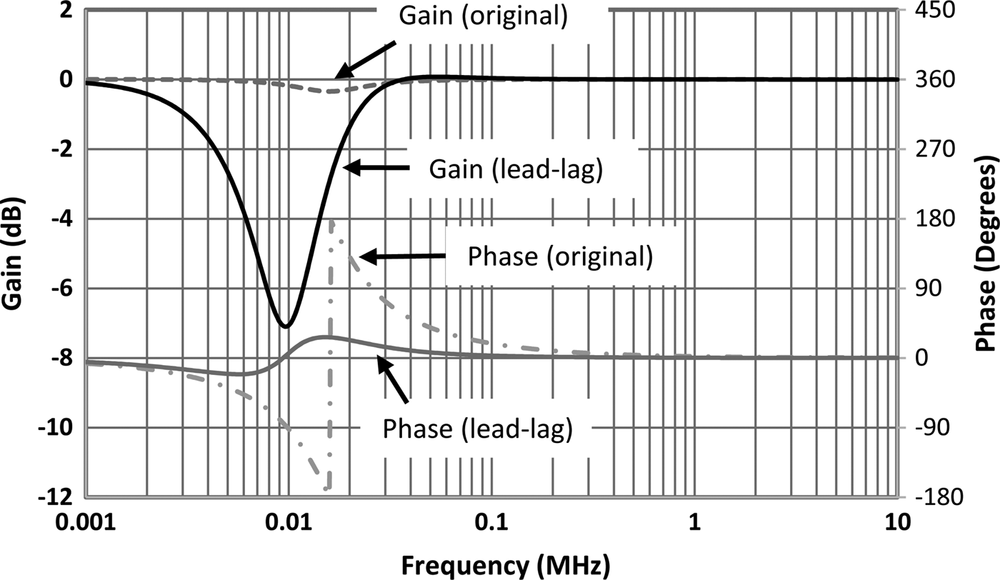
In this work, R L has a value of 10 Ω – an appropriate value for RF PA drain impedance for an RF PA with an output power in the region of 20 W [Reference Watkins8]. The lead-lag modulator is designed with the same value of L 2 as the original split frequency modulator and SMPS input filter (L 1 and R 2), but C 4 is increased by a factor of 3 as previously explained. Apart from the introduction of R 3, the low-frequency path is unchanged. A small signal simulation of the two modulators was carried out in Advance Wave Research's Virtual System Simulator, the results of which are shown in Fig. 3.
Fig. 3. Simulated small signal frequency response of modulators.
The original modulator was tuned for a flat gain response as proposed in [Reference Raab5], but it still incurs the 360° phase transient. In comparison, the phase transient of the lead-lag modulator is significantly reduced. The null resulting from the lead-lag architecture when the paths are in anti-phase due to current limiting is clearly shown in Fig. 3. The crossover frequency is also shifted to 9.3 kHz by the lead-lag design.
The importance of modulator frequency response can be best demonstrated when simulating the transfer response with a wideband LTE envelope signal. For this work a 3 MHz bandwidth signal was used, which is the maximum operating bandwidth of the modulator used in the practical section of this work. Signal fidelity is evaluated with the normalized root-mean-square error (NRMSE) [Reference Hong, Mukai, Gheidi, Shinjo and Asbeck9], which is a comparison of the input and output signals. The NRMSE is calculated from the root-mean-square error (RMSE) with:
 $$NRMSE = \displaystyle{{RMSE} \over {{V_{out,max}} - {V_{out,min}}}},$$
and the RMSE is:
 $$RMSE = \sqrt {\displaystyle{{\sum\nolimits_{t = 1}^n {{{\left( {{V_{out,t}} - \alpha {V_{in.t}}} \right)}^2}}} \over n}},$$
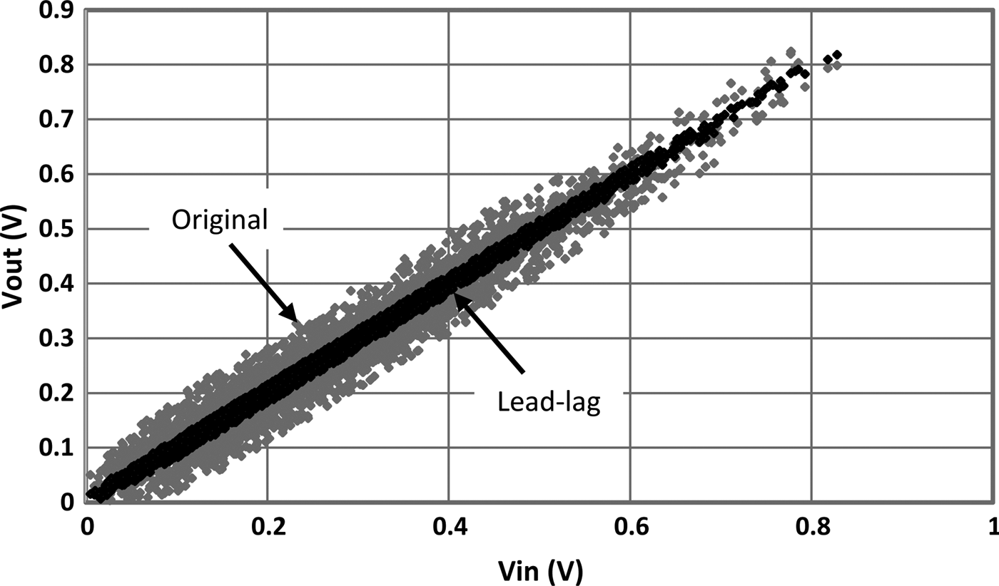
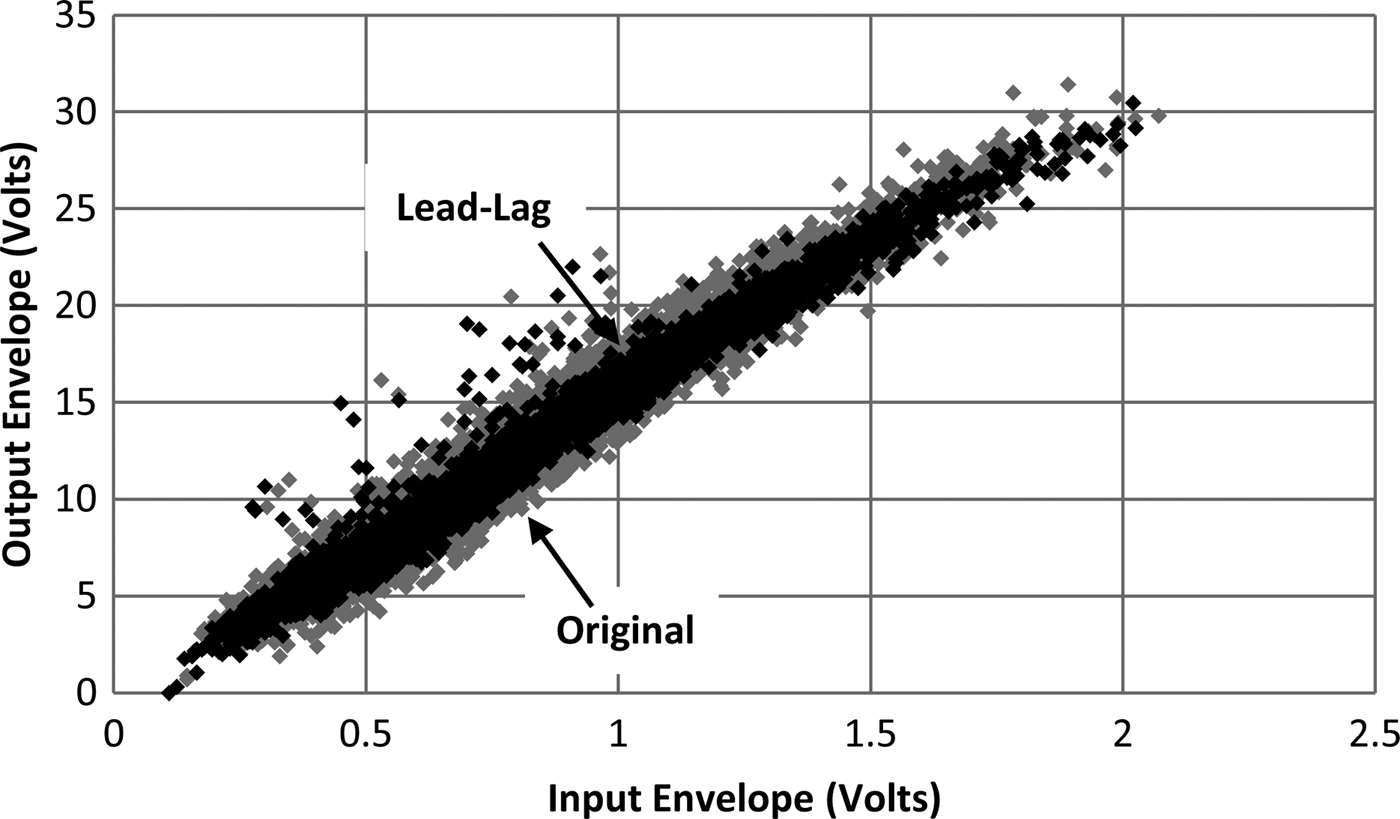
where α is a gain constant used to normalize the input voltage (V in) with respect to the output (V out). V out,max and V out,min are the maximum and minimum values of V out. The NRMSE of the original split frequency modulator (Fig. 1) was calculated as −27.3 dB and that of the lead-lag as −39.2 dB. The transfer response of both modulators is shown in Fig. 4. From Fig. 4, it can be surmised that the spreading of the points of the original modulator's transfer response are due to the phase transient at the crossover region. The reduced phase transient of the lead-lag modulator results in far less spreading. It should be noted that the SMPS and Linear Amplifier used in this simulation are ideal, i.e. infinite bandwidth and free of non-linear distortion.
Fig. 4. Simulated transfer response of original and lead-lag modulators.
The distortion introduced by the timing misalignment between the RF and modulator paths will degrade the error vector magnitude and the adjacent channel power ratio at a transmitter output. It has previously been shown that any irregularities in envelope modulator response – both linear [Reference Kato, Funahashi, Yamaoka, Yamaguchi, Jiafeng, Morris and Watkins10] or non-linear [Reference Hassan, Larson, Leung and Asbeck11] – can also degrade RF performance. The null in the gain response of the lead-lag modulator as shown in Fig. 3 has less of an impact on the modulator response than the phase transient, justifying the benefit of the lead-lag architecture.
The simulation was also performed with a 20 MHz LTE signal. Under these conditions the NRMSE of the original modulator was −33.3 dB and the lead-lag −37.1 dB, resulting in a 3.8 dB improvement. This is less than the improvement found with a 3 MHz bandwidth signal because as the envelope signal bandwidth increases, the distortion at the crossover region affects a smaller proportion of the signal. Hence the impact of the distortion is less significant. However in the future it will be preferable to increase the crossover frequency as SMPS switching frequency increases, since this will reduce the value and physical size of L 1, L 2, and C 4 in Fig. 2(h). However, doing this also increases the impact of the distortion originating from the crossover region.
Although linearity is enhanced by the inclusion of R 3 in Fig. 2(h), efficiency is severely degraded since half of the SMPS output voltage is dropped across it. Reducing R 3 improves efficiency, but the magnitude of the phase transient also increases until it approaches that of the original split frequency modulator. A technique for overcoming this issue is described next.
V. SYNTHETIC IMPEDANCE
R 3 and R L in Fig. 2(h) form a potential divider at the SMPS output. In this work, they are equal in value, therefore halving the efficiency of the low-frequency path. Replacing R 3 with synthetic impedance [Reference Jordan12] maintains the efficiency. Synthetic impedance simulates a resistor using a combination of current and voltage feedback around an amplifier. Current feedback is achieved by measuring the voltage drop across a sense resistor. Any voltage dropped across this resistor is dissipated as heat, therefore reducing efficiency. For example, if the sense resistor is 2% of R L approximately 2% of the output voltage will be dropped across the sense resistor and the efficiency of the SMPS path reduced by a similar amount.
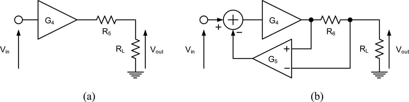
To calculate the amount of feedback needed; an amplifier with gain G 4, an output impedance R 5 and load R L is compared with the equivalent synthetic impedance circuit composed of G 4, G 5, R 6 (the sense resistor), and R L in Fig. 5(b).
Fig. 5. Potential divider formed at SMPS output (a) and equivalent circuit using a synthetic impedance (b).
R 5 and R L in Fig. 5(a) form a potential divider so that:
 $${V_{out}} = \displaystyle{{{G_4} \cdot {R_L} \cdot {V_{in}}} \over {{R_L} + {R_5}}}.$$
Figure 5(b) uses feedback via G 5 to produce:
 $${V_{out}} = \displaystyle{{{G_4} \cdot {R_L} \cdot {V_{in}}} \over {{R_L} + {R_6} \cdot ({G_4} \cdot {G_5} + 1)}},$$
(23) and (24) can be equated to derive G 5 as:
 $${G_5} = \displaystyle{{{R_5} - {R_6}} \over {{R_6} \cdot {G_4}}}.$$
Although it is desirable to reduce the value of R 6 as much as possible to increase efficiency, excessive gain of G 5 could lead to instability [Reference Cantrell13].
VI. IMPLEMENTATION
Although the synthetic impedance is not crucial to improving linearity, without it the modulator would be inefficient, and the resulting ET transmitter offer no efficiency enhancement compared to a non-ET transmitter. Because of this, the synthetic impedance shall be described and evaluated first before the complete modulator.
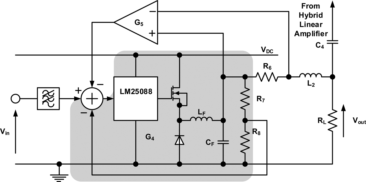
The synthetic impedance was implemented around a Texas Instruments LM25088 SMPS [Reference Watkins8]. A simplified schematic of the SMPS is shown in Fig. 6, where the components within the shaded area are equivalent to G 4 in Fig. 5. Voltage feedback to the SMPS is provided by the potential divider formed by R 7 and R 8 and current feedback by G 5. The output filter of the SMPS is formed by L 2 and C 4 with a cut-off of 15.9 kHz.
Fig. 6. Simplified schematic of SMPS, the components in the shaded area are equivalent to G 4.
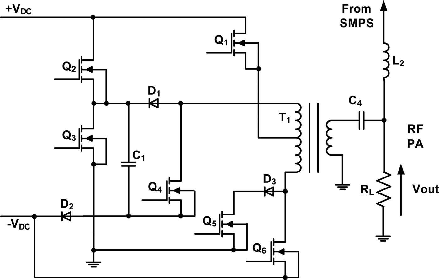
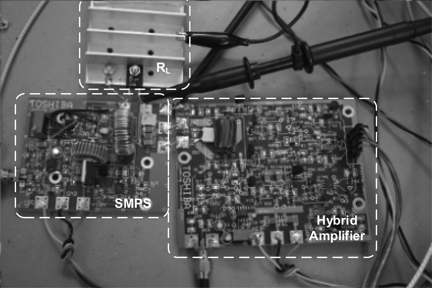
The SMPS is combined with an existing high-efficiency modulator based around the hybrid analog/switching Linear Amplifier shown in Fig. 7. The hybrid amplifier consists of two switching sections; Q 2, Q 3, and Q 4 responsible for amplifying the positive excursions of the high-frequency content of the envelope signal, and Q 5 and Q 6 for the negative. The high-frequency content is asymmetric, i.e. the amplitude of its peak positive excursion is 1.5 times that of the negative for a 7 dB PAPR signal [Reference Watkins8]. Alternative ends of transformer T 1 are terminated with a plurality of voltages to recreate the positive and negative excursions of the AC signal. Q 1 passes a linear signal to fill in the gaps caused by the switching action. The switching transistors are ZVN2110A [14] and Q 1 which is a linear device is an LDMOS PD85004 RF device [15]. A photograph of the prototype modulator is shown in Fig. 8, including the SMPS with a synthetic output impedance, hybrid modulator, and the load R L.
Fig. 7. Simplified schematic of hybrid amplifier (G 3).
Fig. 8. Photograph of prototype modulator.
VII. RESULTS
A) Synthetic impedance
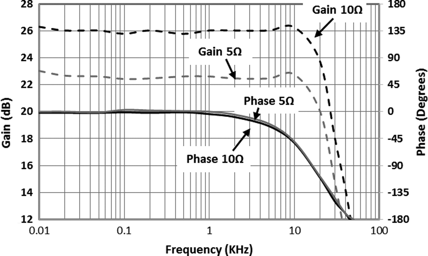
The synthetic impedance was characterized by applying a DC input so that SMPS's output voltage was at the mean value of 13.5 V – a typical mean operating point for a practical ET RF PA. A sinusoid was superimposed upon this. The frequency of this sinusoid was swept from 10 Hz to 50 kHz with the 10 Ω load. Then the 10 Ω load was replaced with a 5 Ω resistor and the measurements repeated under the same input signal conditions. The SMPS frequency responses for both loads are shown in Fig. 9.
Fig. 9. SMPS frequency response with 5 and 10 Ω loads.
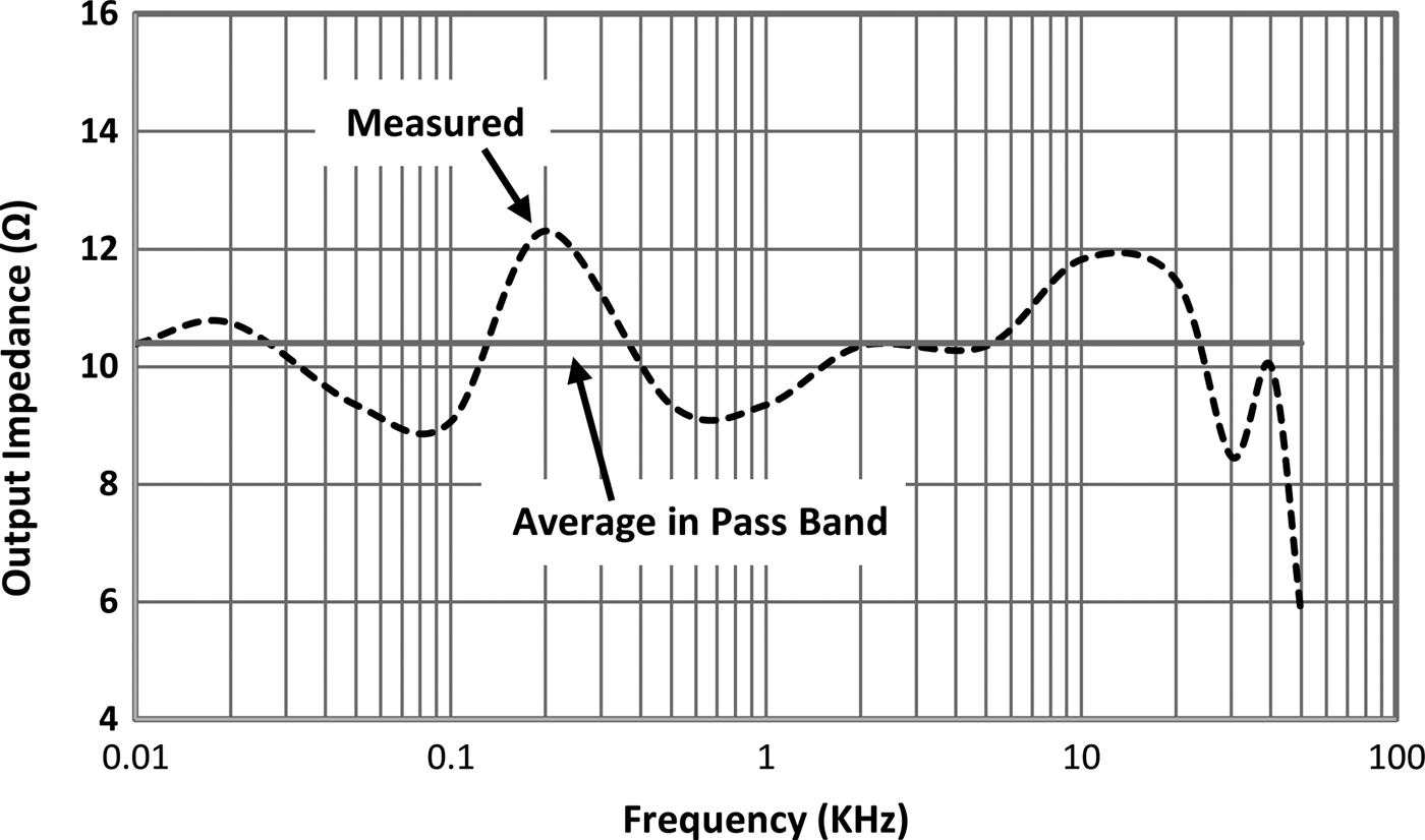
Due to the potential divider formed by the output impedance and the load, there should be a 3.5 dB difference in gain between the 10 and 5 Ω loads, similar to that observed in Fig. 9. The phase response with both loads is essentially identical, suggesting that the synthetic impedance is purely resistive. A reactive output impedance would result in a difference in the phase responses. The bandwidth with both loads is 22 kHz. By comparing the gain responses of Fig. 9 the output impedance is calculated as shown in Fig. 10.
Fig. 10. SMPS output impedance derived from Fig. 9.
Due to the low measurement frequency, a vector network analyzer could not be used to measure the gain and phase response, so this was done manually with a Tektronix AFG3101 function generator and a LeCroy WaveAce 222 oscilloscope. The oscilloscope had a vertical accuracy of ±3%. This will introduce errors to the voltage measurements and could likely account for the large ripple visible in Fig. 10. Over the 22 kHz pass-band the output impedance fluctuates between 8.8 and 12.3 Ω corresponding to an average value of 10.4 Ω.
B) Modulator frequency response
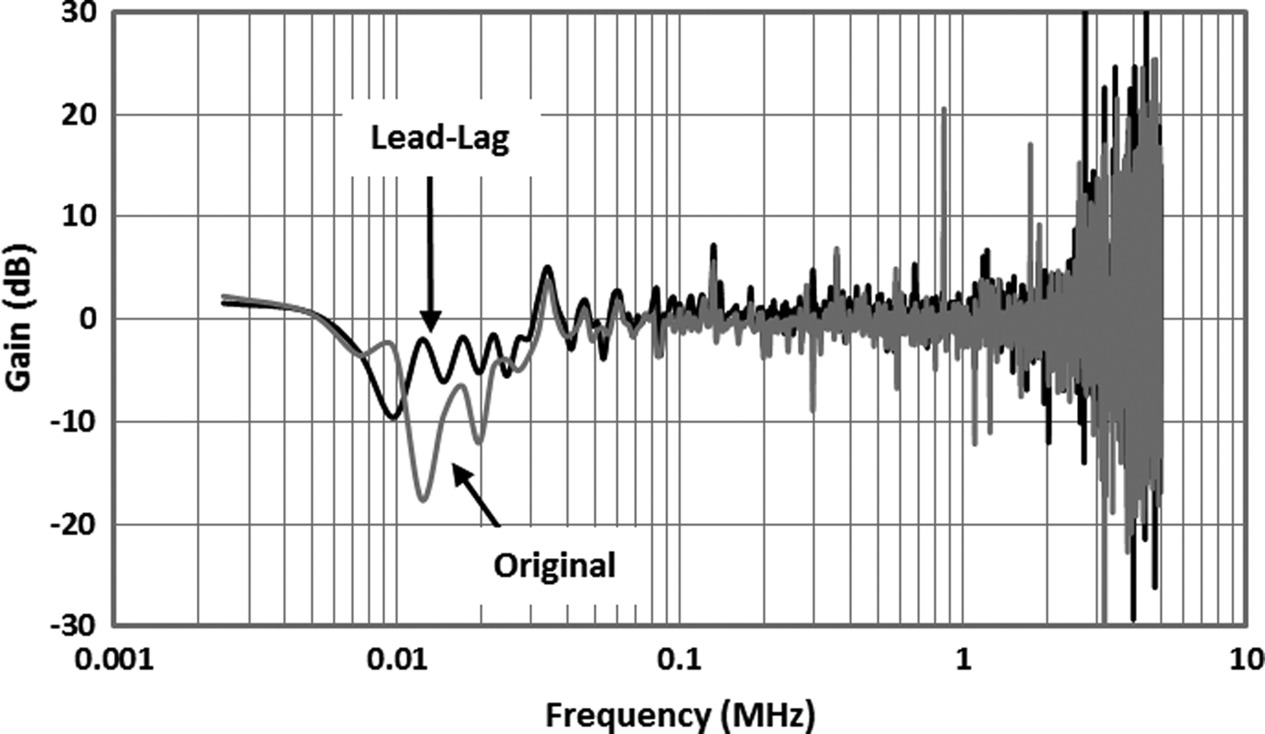
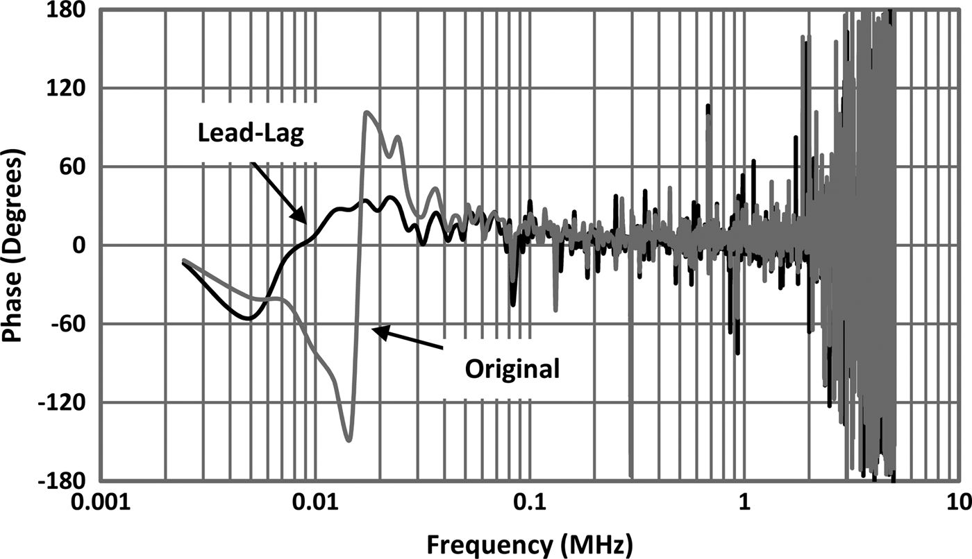
It is not possible to perform a conventional small signal frequency sweep of the modulator due to the hybrid Linear Amplifier (G 1 in Fig. 1 and G 3 in Fig. 2(h)) and the baseband processing required for its digital control signals which are calculated off-line in this work. Instead the dynamic frequency response was measured by applying the 3 MHz bandwidth LTE signal to the modulator and performing a fast Fourier transforms (FFT) on the input and output captured waveforms. The FFTs were subtracted from one another to determine the gain and phase responses shown in Figs 11 and 12. Under these conditions the modulator delivered 23.7 W into the 10 Ω load.
Fig. 11. Dynamic gain response of the modulators with 3 MHz bandwidth LTE signal.
Fig. 12. Dynamic phase response of the modulators with 3 MHz bandwidth LTE signal.
It should be noted that the limited output current of the SMPS and hybrid linear amplifier in the original split frequency modulator resulted in a null in the flat gain response around the crossover region as predicted. For these results the FFT bin size was 2.44 kHz (10 Msps/4096) which limits the resolution at the lower end of the frequency response. The phase transient can however be seen to be significantly reduced to −57° and +36°, and the crossover frequency shifted to 8.5 kHz.
The inclusion of 10.4 Ω synthetic impedance reduced the modulator efficiency slightly from 83.0 to 81.6%. If a synthetic impedance had not been used as shown in Fig. 5(a), then the final modulator efficiency would have been 49%.
The degradation in response at the upper ends of Figs 11 and 12 is due to the switching noise of the modulator. At low frequencies any timing misalignment between the stages is small, but as frequency increases it becomes more significant. The transfer response of the original split frequency and the lead-lag modulators is shown in Fig. 13.
Fig. 13. Measured transfer response of modulators.
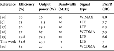
From Fig. 13 the NRMSE can be seen to improve by 2.5 dB from −27.5 to −30.0 dB, less than the 11.9 dB of the simulated results. This is largely due to out-of-band switching noise, which will tend to spread the points of the transfer response. There is also likely to be an impact of the modulator's finite frequency response, which has been shown to introduce distortion if not accounted for [Reference Kato, Funahashi, Yamaoka, Yamaguchi, Jiafeng, Morris and Watkins10]. To test this, both modulators were also tested with a 1.4 MHz bandwidth LTE signal. Under these conditions the NRMSE improved by 3.6 dB from −27.1 to −30.7 dB. This small improvement suggests that dominant factor is not the bandwidth of the modulator, but its switching noise. The NRMSE reported here is less than that of similar work, for example, in [Reference Hong, Mukai, Gheidi, Shinjo and Asbeck9], but that is for low-power (3.3 W) modulator based on a full signal bandwidth SMPS. Also, although [Reference Hong, Mukai, Gheidi, Shinjo and Asbeck9] is more linear, it has a lower efficiency of 73% compared with the 81.6% of this work.
Compared with the similar published work, the modulator performs favorably with others in its class as shown in Table 1. Only one of the wideband code division multiple access (WCDMA) modulators [Reference Aitto-Oja18] has a higher efficiency. It is not appropriate though to compare the results for an ET modulators optimized for LTE with one for WCMDA since the two signals have different characteristics. Approximately 80% of an LTE's envelope signal power falls within the SMPS's bandwidth, whereas for WCDMA it is 93% [Reference Warr, Morris, Watkins, Horseman, Takasuka, Uedo, Kobayashi and Miya21]. LTE also has a larger PAPR than WCDMA. Though [14] is valid, since WiMAX uses orthogonal frequency division multiplexed modulation like LTE, so can be considered similar.
Table 1. Comparison of similar envelope modulators.
VIII. CONCLUSION
In this paper, we propose a new envelope modulator architecture based on a lead-lag network. It is intended to improve the frequency response in the crossover region compared with the original split frequency type. In simulation, the NRMSE is improved by 11.9 dB from −27.3 to −39.2 dB.
The lead-lag modulator includes a resistor in the output of the low-frequency path. This would severely impact system efficiency. To counteract this, a synthetic impedance is implemented using current and voltage feedback around an SMPS. Over the low-frequency path bandwidth, the synthetic impedance had an average value of 10.4 Ω.
Overall modulator dynamic frequency response was evaluated by applying a 3 MHz bandwidth LTE envelope signal to the modulator and calculating the spectrum of the input and output signals. The lead-lag architecture is found to have a flatter frequency response than the original modulator, with reduced gain and phase distortion in the critical crossover region. Practically the NRMSE was improved from −27.5 to −30.0 dB. Total modulator efficiency was 81.6% at 23.7 W mean envelope power. These results compare favorably with other published works.
ACKNOWLEDGEMENTS
The author would like to thank all at Toshiba's Telecommunications Research Laboratory for their support in this work.
 G. T. Watkins is a member of both the Institute of Engineering Technology and the European Microwave Association. He received his M.Eng. degree in Electrical and Electronic Engineering in 2000 from the University of Bristol and a Ph.D. degree from the same institution in 2003 on the topic Wideband Feedforward Amplifiers for Software-defined Radios. From 2003 to 2004, he was a Technical Consultant for Detica Information Intelligence before joining the University of Bristol as a Research Associate. Since 2008 he has been with Toshiba Research Europe Limited where he is currently a Principal Research Engineer and team leader. His research interests include linear power amplifiers, high-efficiency system architectures, analog circuitry, high-speed power switching architectures, and wideband RF structures.
 K. Mimis received his M.Sc. and Ph.D. degrees from the University of Bristol, Bristol, UK in 2008 and 2013, respectively. Since 2012 he has been with Toshiba Research Europe Limited, Bristol, UK. His research interests include high-efficiency, broadband power amplifier design, amplifier linearization, and efficiency enhancement techniques.