I. INTRODUCTION
Radio-frequency (RF) wireless communication systems that are used to send and receive information are common in modern society. To obtain a more advanced system with lower costs, the integrated circuits must be more highly compacted. In recent years, the CMOS process has been used to design RF circuits, because the process technology has been improved. The front-end RF circuit has been designed to realize system on chip (SoC), which is now possible in the CMOS process [Reference Abidi1]. The high performance of a local oscillator (LO) is very important and can stabilize the system as well as increase power transfer from DC to AC signal efficiency in wireless transceivers. Therefore, how to design a high-performance (low-power, wide tuning-range, low-phase noise, and small area) voltage-controlled oscillator (VCO) is an important issue of communication application.
Recently, the low-power LC VCOs topology has been reported [Reference Park and Cho2–Reference Kwok and Luong7]. There has been much research on low-voltage operation with transformer feedback [Reference Hsu and Huang3, Reference Chiu, Lin and Chang4, Reference Kwok and Luong7], lower power with body bias [Reference Park and Cho2] or current-reused topology [Reference Chuang, Jang, Senior, Lee, Yen and Jhao5] and low-phase noise with Q-improvement techniques [Reference Park, Lee, Choi and Hong8]. Since lower-power consumption saves energy to enhance the device or system efficiency, this proposed circuit is designed for low power consumption with the body-biasing technique and low-phase noise with the Q-improvement technique. Analysis and a detailed circuit design of the proposed circuit have been addressed in the paper. The phase noise issues are described in Section II. The proposed VCO topology with formula derivation for negative resistance and body-biasing technique and Q-enhancement is presented in Section III. The measurement results are shown in Section IV. Finally, the conclusion is described in Section V.
II. PHASE NOISE ISSUE
It was in early 1997 that researchers came to realize a fully integrated LC-tank N-type metal-oxide-semiconductor (NMOS) VCO [Reference Craninckx and Steyaert9]. In the high-frequency operation regime, the NMOS device is viewed as a high-noise device because of its high density of the majority carriers. Therefore, the P-type metal-oxide-semiconductor (PMOS) device has been replaced by the NMOS to reduce phase noise because of its lower flicker noise at lower frequencies. In addition, the PMOS transistor has lower flicker noise than that of NMOS transistor. This property will give rise to reduce phase noise (by up-conversion) than that of only NMOS transistor VCO. For the purpose of symmetrical signal output swing, the complementary P/N MOS cross couple VCO has good performances than that of only PMOS VCO or NMOS VCO. Of course, the output voltage of signal swing can also reach double ratio with V DD supply. Therefore, the complementary cross-couple VCO is popular for circuit design with high performance [Reference Han and Hajimiri10]. But, there are some drawbacks that include an unsymmetrical output signal, switching speed that becomes slower than the NMOS, instability coming from the V DD variation and interference noise.
Figure 1 is a complementary cross-coupled LC-tank with fixed-bias (FB) tail transistor VCO, which is composed of the NMOS and PMOS cross-coupled pairs. There are three excellent properties as described in the following [Reference Han and Hajimiri10]:
-
1. Same current existing, so that the complementary cross-coupled pair offers higher transconductance and faster switching speed on each side.
-
2. The rise-time and the fall-time are more symmetrical to each other, for consideration to prevent the excess noise, which comes from low-frequency noise 1/f, transferring to high frequency.
-
3. In all NMOS pairs, the channel voltage is higher, which causes a faster saturation speed and a higher γ value (γ is a fabrication-process parameter).
As shown in Fig. 1, M1–M4 consist of a complementary cross-coupled pair, which yields negative resistance to compensate for the loss of the non-ideal LC tank and whose outputs are differential. Figure 1 also shows that the P/N cross-coupled topology can reduce the impulse sensitivity function (ISF) because of its symmetrical output signal. The tail transistor M5 is designed to operate in the saturation region as a current source. Consequently, the tail current determines the oscillation amplitude.
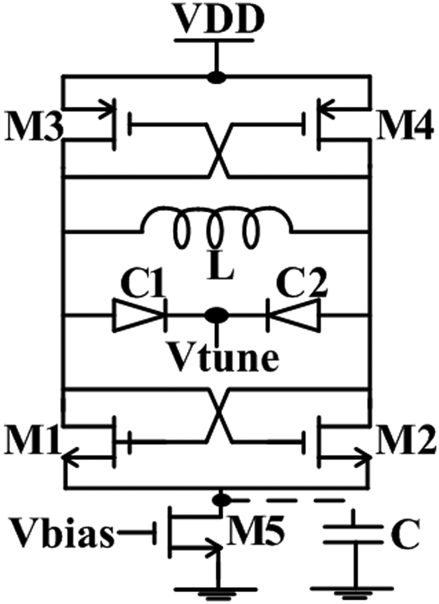
Fig. 1. FB tail transistor VCO with and without capacitor.
In the VCO, the generation of phase noise results from various reasons. But, there are only certain parts of the noise sources that contribute significantly to the total phase noise [Reference Rael and Abidi11]. It should be noted that phase noise is not caused mainly by up-conversion or down-conversion. Finally, the tail current source, which is well known, is a large noise source in a VCO. Flicker noise sources will be up-converted to AM noise, and then go into phase noise by amplitude-modulation-to-phase-modulation (AM–PM) conversion of varactors and capacitors dependent on voltage, and thermal noise sources will be converted into phase noise, due to the switching mechanism of the cross-coupled pair as a single-balanced mixer [Reference Hegazi, Sjoland and Abidi12]. These noise sources go into output phase noise by up-conversion and down-conversion. Generally, thermal noise will be converted into 1/f 2 region, and flicker noise will be converted into 1/f 3 region [Reference Hajimiri and Lee13]. Table 1 shows the phase noise contribution of each part in the VCO circuit.
Table 1. Phase noise contribution of each part in the VCO circuit.

The tail transistor source only gave thermal noise in the current-source transistor around the second harmonic of the oscillation. Moreover, high impedance was viewed at the tail that required the stopping of the cross-couple PMOS/NMOS in the triode at the second harmonic from loading the resonator. This suggests that a narrowband circuit is required to suppress the troublesome noise frequencies in the current source, making it appear noiseless to the oscillator, which gives high impedance in the narrow band of frequencies. Therefore, we can put a capacitor into the circuit in parallel with the current source, as shown in Fig. 1 [Reference Hegaji, Sjoland and Abidi14]. This technique is also called the tail current-shaping technique for LC-VCO application [Reference Soltanian and Kinget15].
Figure 2 shows the self-bias (SB) tail transistor VCO. The operation of the novel oscillator is as follows. Initially, when the circuit is balanced, both the output voltage and current flowing in the two sides are set by the size of the tail transistors. The tail transistors will go into the saturation region first while the cross-coupled NMOS transistors are still in the cutoff region. When both the tail transistors and cross-coupled NMOS transistors are in the triode region, the tail transistors determine the current as the voltages at the source of the cross-coupled NMOS transistors are floating. Since all the transistors in this VCO topology are switched biasing rather than fixed biasing, it is expected to have lower flicker noise [Reference Klumperink, Gierkink, van der Wel and Nauta16, Reference Gierkink, Klumperink, van der Wel, Hoogzaad, van Tuijl and Nauta17]. Moreover, as the transistors operate in the triode region for a large portion of the oscillation period, they exhibit lower current flicker noise than the transistors that operate in the saturation region, for example, the tail transistor in the FB topology [Reference Hung, Ko, Hu and Cheng18].

Fig. 2. SB tail transistor VCO.
In this paper, we added two merits in the circuit. The first is the SB of the tail current transistor and the capacitance ground filter technique, which are combined to improve the phase noise performance. The second is the body-biasing technique of the cross-couple transistor to reduce the power consumption.
III. CIRCUIT DESIGN
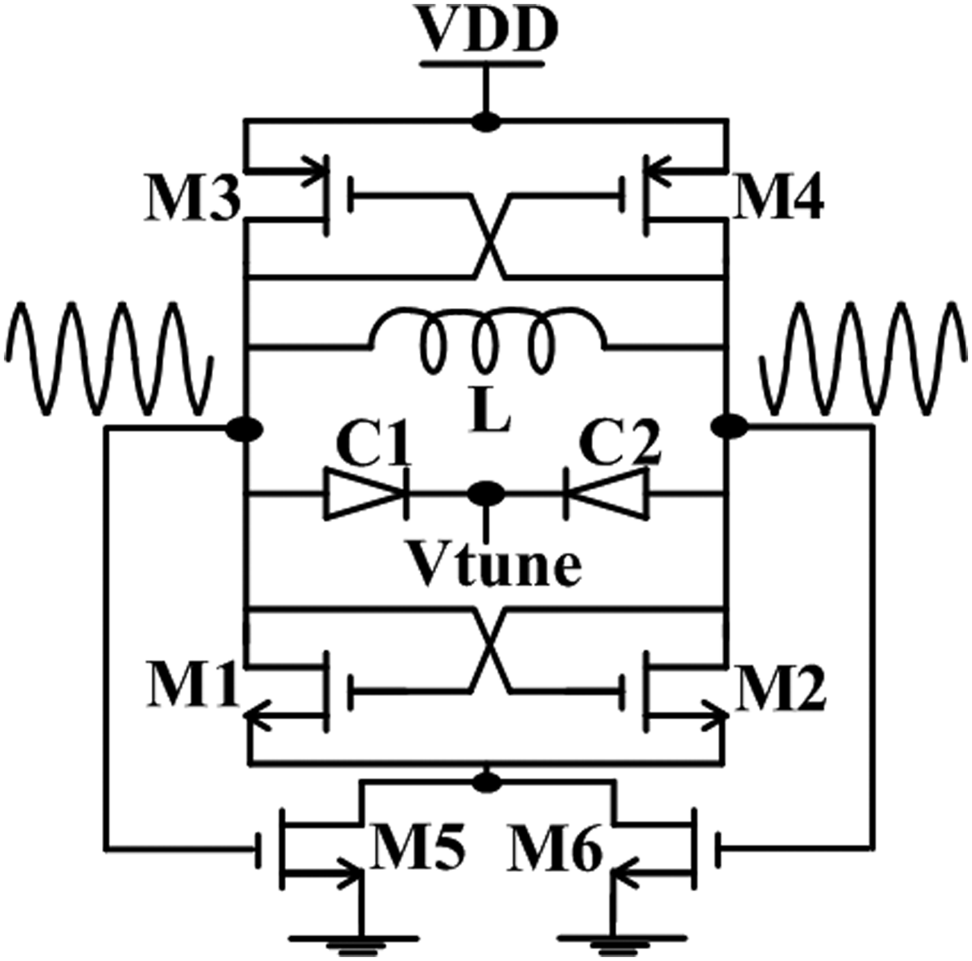
The proposed low-power consumption VCO is realized by the body-biased and Q-enhancement techniques. The schematics of the proposed VCOs are shown in Fig. 3. All those circuits are designed with the body-biasing technique. Figure 3(a) shows the chip with Q-enhancement in terms of capacitors C1/C2 and transistors M3, M4, M5 and M6. Figure 3(b) shows the circuit without Q-enhancement.
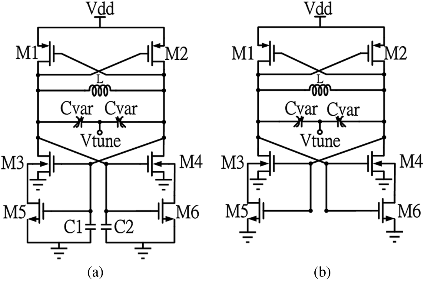
Fig. 3. Schematic diagrams of the two VCOs, (a) chip with Q-enhancement circuit and (b) non-Q-enhancement circuit.
A) LC tank
The oscillation frequency is generally determined by tanks. The first consideration of LC tanks fabrication is inductor design, which is more difficult than the capacitance. In order to have a wide tuning range, it is desirable for the inductor L to be small compared to the varactor C var , and have low parasitic capacitance such as metal-to-substrate capacitance and metal-to-metal capacitance. Furthermore, as the operating frequency is raised, then quality factor Q increases and inductor loss decreases. This VCO uses a two-loop inductor, which can provide enough inductance and also has a high-quality factor for the resonator to operate with fundamental circuit topology from 4.92 to 5.7 GHz. A 0.7 nano-Henry spiral inductor is implemented in this chip. The inductor has a quality factor of approximately 12.3 at the working frequency 5 GHz. The inductance and quality factor of the inductor are shown in Fig. 4.

Fig. 4. Inductance and quality factor.
The capacitance range of the MOS varactor [Reference Andreani and Mattisson19] is wider than the junction varactor and the equivalent series resistance of the former is smaller than that of the latter. Because an NMOS varactor does not lie in a P-well, the NMOS varactor is apt to be disturbed in substrate. The concentration of the dopant in the N-well is bigger than that in the P-bulk, which reduces interference as far as the PMOS varactor is concerned. In view of this, we have adopted the PMOS varactor.
B) Body-biasing technique
In many integrated circuit applications, the source terminal is connected to the body (substrate) terminal. According to Adel et al. [Reference Adel and Sedra20], the body-effect equation can be indicated as follows:
 $$V_t=V_{t0}+\gamma \left({\sqrt {2\varphi _f+V_{sb} } - \sqrt {2\varphi _f } } \right)$$
and
 $$\gamma=\sqrt {\displaystyle{{2qN_A \varepsilon _S } \over {C_{OX} }}}$$
where V t0 is the threshold voltage for source–body voltage V sb = 0; ϕ f is a physical parameter; γ is a fabrication-process parameter, q is the electron charge (1.6 × 10⁻¹⁹ C), N A is the doping concentration of a p-type substrate, and ε S is the permittivity of silicon. Equation (1) indicates that an incremental change in V sb will give rise to an incremental change in V t . In other words, when the V sb source-body voltage is reduced, the MOSFET required threshold voltage V t is lessened, too. Besides, the MOS current consumption can be reduced. The body-biasing technology can reduce the MOS threshold voltage V t to decrease the drain–source current which will produce sufficient transconductance (g m ) [Reference Park and Cho2]. Figures 5 and 6 are high-frequency small signal models of MOS. Figure 5 shows the MOS in which the source terminal is connected with the body terminal. The equivalent transconductance (g m ) of this MOS model can be indicated as follows [Reference Adel and Sedra20]:

Fig. 5. The case body-source terminal is connected for high-frequency small signal model of MOS.

Fig. 6. The case body terminal and source terminal is divided for high-frequency small signal model of MOS.
 $$g_m=\mu _n C_{ox} \displaystyle{W \over L}\left({V_{GS} - V{}_t} \right)$$
without body-biasing technique, the body terminal and source terminal are connected together, so V bs = 0. Moreover, the body-effect can be ignored. Figure 6 is the high-frequency small signal model of MOS in which the source and body terminal are divided. When a bias voltage is applied to the body terminal, then the equivalent transconductance can be rewritten as follows [Reference Adel and Sedra20]:
 $$g_{mb}=\mu _n C_{ox} \displaystyle{W \over L}\lpar V_{GS} - V{}_t\rpar \left({\displaystyle{\gamma \over {2\sqrt {2\varphi _f - V_{bs} } }}} \right).$$
Furthermore, it produced extra body-transconductance (g mb ) in the MOS equivalent transconductance (G m ), when the MOS body terminal has the appropriate bias applied. The formula for MOS equivalent transconductance (G m ) is shown as follows [Reference Allen and Holberg21]:
 $$G_m=g_m+g_{mb}\comma$$
where g m is MOS transconductance from the V GS bias, g mb is MOS body transconductance from the V bs bias. Compared to the general connect body–source terminal MOS, body-biasing can give larger negative conductance with a less V GS biased condition. The body-biasing technology also can indirectly improve the VCO phase noise under switched MOS gate conditions [Reference Šiprak, Zanolla, Tiebout, Baumgartner and Fiegna22].
C) Q-enhancement circuit
The proposed VCO based on complementary cross-coupled topology is shown in Fig. 3(a), the simple schematic of the proposed Q-enhancement circuit is shown in Fig. 7 and its equivalent low-frequency model with body-biasing is shown in Fig. 8.

Fig. 7. Simple schematic of proposed Q-enhancement circuit.

Fig. 8. Equivalent low-frequency model with body-biased of Q-enhancement circuit.
By considering the equivalent low-frequency model with a body-biased of Q-enhancement circuit (Fig. 8), we have
 $$Vx=V_3 - V_4\comma$$
 $$I_X=g_{m4} V_4+g_{m6} V_4+g_{mb4} V_{bs4}+sC_1\, V_3\comma$$
then we have
 $$I_X+\lpar g_{m4}+g_{m6} \rpar V_X - g_{mb4} V_{bs4}=V_3 \lpar g_{m4}+g_{m6}+sC_1 \rpar$$
and
 $$V_3=\displaystyle{{I_X+\lpar g_{m4}+g_{m6} \rpar V_X - g_{mb4} V_{bs4} } \over {g_{m4}+g_{m6}+sC_1 }}.$$
In this work, a symmetric structure is adopted, thereby g m3 = g m4 = g mx , g m5 = g m6 = g my , sC 1 = sC 2 = sC, then (9) becomes (10)
 $$V_3=\displaystyle{{I_X+\lpar g_{mx}+g_{my} \rpar V_X - g_{mb} V_{bs4} } \over {g_{mx}+g_{my}+sC}}.$$
By the same method, we can obtain (11)
 $$V_4=\displaystyle{{I_X+\lpar g_{mx}+g_{my} \rpar V_X - g_{mb} V_{bs3} } \over {g_{mx}+g_{my}+sC}}.$$
Substituting (10) and (11) into (6), we obtain
 $$V_X=\displaystyle{{2I_X+2\lpar g_{mx}+g_{my} \rpar V_X+g_{mb} \lpar V_{bs3} - V_{bs4} \rpar } \over {g_{mx}+g_{my}+sC}}.$$
If we assumed that V bs3 = V bs4 = V bs , then equation (12) become as (13)
 $$V_X=\displaystyle{{2I_X+2\lpar g_{mx}+g_{my} \rpar V_X } \over {g_{mx}+g_{my}+sC}}\comma$$
we can arrange (13) to obtain (14) of input admittance
 $$Y_{in}=\displaystyle{{I_X } \over {V_X }}=\displaystyle{{ - \lpar g_{mx}+g_{my} \rpar +sC} \over 2}$$
substituting s = jω from (14), we can obtain
 $$Y_{in}=\displaystyle{{ - \lpar g_{mx}+g_{my} \rpar } \over 2}+j\displaystyle{{\omega C} \over 2}$$
and
 $$Z_{in}=\displaystyle{1 \over {Y_{in} }}.$$
If the admittance Y in = G n + jB n is taken into equation (16), then we can have the following equation:
 $$Z_{in}=\displaystyle{1 \over {G_n+jB_n }}$$
where
 $$G_n=- \displaystyle{{g_{mx}+g_{my} } \over 2}$$
is the real part of the admittance of the active circuit, and
 $$jB_n=s\displaystyle{C \over 2}=sC_{in}$$
is the imaginary part of the admittance of the active circuit.
Figure 9 shows the one-port equivalent circuit of the general VCO between passive and active circuits. G n indicates the negative transconductance of M3/M4 NMOS transistor with the low-frequency model. Assume that the resistance of the LC tank is represented R p , which is in parallel with the LC resonance circuit, then the start-up condition of the proposed VCO can be obtained as the following equation:

Fig. 9. One-port equivalent circuit of VCO between passive and active circuit.
 $$R_p+G_n \leq 0.$$
The oscillation frequency ω0 with Fig. 9 also can be calculated by the following equation:
 $$\omega _0=\displaystyle{1 \over {\sqrt {L\left({C_{{\mathop{\rm var}} }+C_{in} } \right)} }}\comma$$
where C var is the varactor capacitor and equivalent capacitor C in is the input capacitor of the proposed VCO with active circuit, then the Q of proposed VCO is the following [Reference Park, Lee, Choi and Hong8]:
 $$Q \approx \displaystyle{1 \over {G_{total} }}\sqrt {\displaystyle{{C_{total} } \over L}}\comma$$
where C total is the total capacitance of VCO, G total is the total conductance of VCO, and L is the inductance of the VCO. Therefore, the VCO total conductance is the following:
 $$G_{total}=G_{loss}+G_n \approx G_{loss} - \displaystyle{{g_{mx}+g_{my} } \over 2}\comma$$
where G loss is the parasitic loss conductance of inductor L, G n is the conductance of NMOS cross-couple pair (M3, M4).
From equation (22), as G total is reduced, then Q of the proposed VCO is increased. Furthermore, the VCO phase noise can be reduced when the quality factor is increased. From Figs 3(a) and 3(b), we observe that the phase noise of the proposed VCO can be improved with the Q-enhancement technique, and the results are shown in Table 2, Fig. 10 and Table 3.
Table 2. Equivalent element value.

Prop. VCO is proposed VCO, and No-Q VCO is without Q-improvement technique VCO.
Table 3. Phase noise of VCO.

Table 2 shows the variation between the VCO with and without Q-enhancement. Figure 10 and Table 3 indicate that the phase noise performance of proposed VCO is better than that of it without Q-enhancement.

Fig. 10. Simulated phase noise of proposed VCO and without Q-improvement technique VCO at 5.1 GHz.
IV. MEASUREMENT RESULTS
The proposed VCOs were fabricated by Taiwan Semiconductor Manufacture Company (TSMC) 0.18-µm 1P6M CMOS technology. An Agilent E5052A signal source analyzer, which administered two DC sources to the supply voltage and control voltage, was used to measure the output frequency, power, phase noise, and output spectrum. The buffers are included on-chip to facilitate driving a 50-Ω environment. Each buffer consists of PMOS transistors and is biased with an external Bias-Tee. The differential outputs connect a Bias-Tee on each side with two loads, Agilent 5052A and 50 Ω.
The die photographs of the chip are shown in Fig. 11. The chip area is 0.692 × 0.537 (mm2). The measured phase noise, output signal spectrum, and frequency-tuning range of the chip are shown in Figs 12–14, respectively. The measured phase noise is −118.05 dBc/Hz at 1 MHz offset from the carrier frequency 4.94 GHz as shown in Fig. 11. The signal output power is about −22 dBm as shown in Fig. 13. The frequency-tuning range is between 4.92 and 5.7 GHz, which achieved a 14.7% tuning range and which is measured from −0.5 to 2 V as shown in Fig. 14. The core power dissipation of the VCO is 2.5 mW with 1.4 V supply voltage.

Fig. 11. Chip photos.

Fig. 12. Measured phase noise.

Fig. 13. Output spectrum.

Fig. 14. Frequency-tuning range.
It is well known that the figure of merit (FOM) is an index between different VCOs [Reference Samori, Lacaita, Villa and Zappa23]. The FOM and FOM t are defined as follows:
 $$FOM=10\log \left[{\left({\displaystyle{{\omega _0 } \over {\Delta \omega }}} \right)^2 \cdot \displaystyle{1 \over {L\left\{{\Delta \omega } \right\}\cdot P_{dc} }}} \right]\comma$$
 $$FOM_t=FOM - 20\log \left[{\displaystyle{{FTR} \over {10}}} \right]\comma$$
where ω0 is the center frequency, Δω is the frequency offset, L{Δω} is the phase noise at Δω, P dc is the dc power consumption. FTR is the frequency-tuning range.
The parameter of our chips and recently reported papers are summarized in Table 4. Most of the VCOs have high FOM of more than −185 dBc/Hz. Focusing on core power dissipation of the VCOs, our work shows good performance for low power applications.
Table 4. Comparison of VCO performance.

1*, Copitts; 2*, PMOS cross-coupled; 3*, NMOS cross-coupled; 4*, P-NMOS cross-coupled; 5*, Transformer; 6*, Body-biasing; 7*, Tail current-shaping technique and body biasing.
V. CONCLUSION
This chip that was adopted using the body-biasing and Q-enhancement techniques for low-power consumption and low-phase noise design has been presented. This chip was implemented in standard 0.18-mm CMOS processes of TSMC. The measurement results show the phase noise −118 dBc/Hz at 1 MHz offset frequency from 4.94 GHz. The core power consumption is 2.5 mW. The FOM of our work shows good performance comparable with other papers in the literature.
ACKNOWLEDGEMENTS
The authors thank the Taiwan Semiconductor Manufacture Company (TSMC) and National Chip Implementation Center (CIC) for the wafer fabrications and IC measurements. This project is supported by the National Science Counsel (NSC 101-2221-E-224-049-).
 Meng-Ting Hsu was born in Changhua, Taiwan, Republic of China in 1961. He received his B.S. and M.S. degrees from Chung-Yuan Christian University in the Electrical and Electronic Engineering in 1989 and 1991, respectively. Since 1992 he has served as a Lecturer in the Electronic Department of National Yunlin University of Science & Technology (NYUST), and he later obtained a Ph.D. degree from National Chiao-Tung University in Communication Engineering in 2004. In 2005, he was promoted to Associate Professor and has more than 15 years experience in microwave circuit design. His current research interests are in noise theory application on MMIC and CMOS RFICs. He is also active on RF UWB design. He is the Vice Dean of Electronic Department of NYUST from August 2011.
 Po-Hung Chen was born in Yunlin, Taiwan, Republic of China in 1987. He received the B.S. degree in Electrical Engineering from Nation Changhua University of Education in 2009. Then, he obtained an M.S. degree from National Yunlin University of Science & Technology (NYUST) in Electric Engineering in July 2011. His present research interests are in RF-integrated circuit design.
 Yao-Yen Lee was born in Taipei, Taiwan, Republic of China in 1987. He received the B.S. degree in Electrical Engineering from Kun Shan University in 2009. He pursues M.S. degree in the National Yunlin University of Science & Technology in Electric Engineering from 2012. His current research interests in CMOS RFICs.