


Introduction
In the current scenario, ultra-wideband (UWB) communication systems offer numerous wideband applications such as microwave medical imaging, ground-penetrating radar, and radio frequency identification tags for inventory control and asset management. The major advantages of a UWB system are to transmit data at a high rate, low energy density, low transmission power requirement, resist jamming, and easy to retrieve error control coding. A UWB transceiver with different blocks is shown in Fig. 1, where the information is encoded first, digitally modulated, and then converted into pulse using a pulse generator [Reference Wang, Zhu and Menzel1], and noise will be removed before transmission by using a UWB band-pass filter (BPF). Design of compact planar BPFs is growing very fast since 2002, whereas the US Federal Communication Commission (FCC) has allowed commercial use of the frequency range 3.1–10.6 GHz [Reference Zhu, Sun and Menzel2]. Hence, various filters had been designed in the past to fulfill the requirement of modern communications, such as short-circuited meandered coupled lines with a rectangular-shaped defected ground structure (DGS) on the ground plane that has been designed to improve the spurious response in stopband [Reference Packiaraj, Vinoy, Ramesh and Kalghatgi3]. The performance of the UWB filter is achieved by combining the spur line, DGS, and split ring resonators, and the same has been used to reduce the size and radiation loss of the filter [Reference Zhou, Zheng and Chan4]. Moreover, the compactness of the filter is also achieved by using an arrowhead DGS [Reference Shaman and Hong5]. Two-stepped impedance resonators and four short-circuited folded stubs are coupled to improve the performance of selectivity of the BPF at lower and higher cut-off frequencies [Reference Nouri, Nourinia, Ghobadi, Alizadeh and Mohammadi6].

Fig. 1. UWB transmitter–Receiver block diagram with bandpass filters.
Meanwhile, some techniques have been reported that enhance the bandwidth of UWB filters such as substrate-integrated waveguide (SIW) technique with loading short and open-ended stubs in the middle section [Reference Li, Ho and Hong7]. Broadside coupled microstrip line and conventional coplanar waveguide structure is used for enhancement of bandwidth [Reference Luo, Ma, Ma and Yeo8]. Similarly, a UWB BPF is designed by using the wave cancellation method which first splits and then combines the signal zero characteristics at lower and higher cut-off frequencies [Reference Gholipoor, Amin Honarvar and Virdee9]. Furthermore, three multi-mode resonators (MMRs) [Reference Zhu, Sun and Menzel2, Reference Ishii, Kimura, Kobayashi, Saito, Ma and Ohshima10] including four folded short-circuited stubs, which are separated by quarter wavelength and semicircle DGSs are utilized to achieve bandpass performance along with excellent band rejection characteristics [Reference Wei, Li, Huang and Shi11]. Wire-bound inter-digitized capacitance is introduced for obtaining strong wideband coupling [Reference Han, Wu and Zhang12] and BPF UWB bandwidth is achieved via microstrip-loaded stubs with an outstanding insertion loss of 0.02 dB [Reference Taibi, Trabelsi, Slimane, Belaroussi and Raskin13–Reference Kamma, Reddy and Mukherjee15]. The DGS is also introduced to enhance the selectivity and sharpness of BPFs [Reference Kumar and Kartikeyan16]. The harmonic suppression technique is used by introducing a parallel-coupled stepped impedance resonator with a varactor diode to increase the bandwidth of the filter [Reference Kumar and Pathak17]. A hairpin structure is designed to achieve high fractional bandwidth [Reference Tripathi, Pathak and Parida18]. A half-mode SIW with a dumbbell-shaped DGS is designed to improve bandwidth of the filter including stopband characteristics [Reference Noura, Benaissa, Abri, Badaoui, Vuong and Tao19–Reference Cao, Han, Chen and Li22].
In this paper, a bandpass filter with good stopband characteristics is achieved by using four combinations of circular/Mickey-shaped stubs (MMR), open-ended transmission line, parallel coupled-line sections, and DGS for UWB bandwidth. The designed filter has achieved better insertion loss and group delay in passband with a minimum value of 0.5 dB and 0.30 ns, respectively, as the proposed filter is fabricated over a cost-effective FR-4 substrate. In the Section “Filter design analysis,” a step-by-step design procedure of the filter is explained. “Results and discussion” section presents the results and current distribution analysis of MMRs including group delay. The conclusion of the proposed design is presented in the Section “Conclusion,” which explains the utility of the UWB BPF in the empirical environment.
Filter design analysis
The proposed UWB BPF is designed and fabricated over an FR-4 substrate having a dielectric constant of 4.4 (tan δ = 0.024) with a substrate height of 1.6 mm. The overall size of the filter is 22 × 20 mm2 as depicted in Fig. 2 after multiple iterations and has simulated using the Computer Simulation Technology tool.
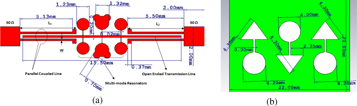
Fig. 2. Proposed geometry of filter: (a) front view and (b) back view.
The design of the filter has a diversely shaped (arrow and circular head) DGS that enhance the pass bandwidth as well as a roll-off rate. This filter also has an MMR mechanism to enhance bandwidth in the passband, which includes two circular Mickey-shaped stub resonators over an open-ended transmission line coupled with parallel microstrip lines at two feeding ends of 50 Ω as shown in Fig. 2.
Figure 3(a) presents the step-by-step geometrical analysis of the proposed UWB BPF with its S-parameters as shown in Fig. 3(b). Filter-1 is designed with the combination of open-ended transmission lines coupled with parallel transmission lines at feeding ends which provide bandpass characteristics in the range of 4–8 GHz, but it is not a good bandpass filter as per the results shown in Figs 3(b) and 3(c), respectively. To further improve the response in passband as well as in stopband, a periodic geometry of DGS is designed in the finite ground plane as shown in Filter-2 and the corresponding results are shown in Figs 3(b) and 3(c), respectively. After the placement of the DGS, the results of Filter-2 are too far away from the intended results; therefore, a Mickey-shaped open stub resonator is connected at the center of the open-ended transmission line as shown in Filter-3 and the corresponding results are near to the intended UWB BPF with compromised return loss at some frequencies as shown in Figs 3(b) and 3(c), respectively. To further improve the response, two circular-shaped open stub resonators are connected at an equal distance from port-1 and port-2 over the open-ended transmission line as shown in Filter-4. Hence, the corresponding 3 dB intended UWB bandwidth is achieved with 20 dB return loss in passband and almost 20 dB insertion loss in stopband as shown in Figs 3(b) and 3(c), respectively.

Fig. 3. Step-by-step geometrical analysis of the proposed UWB bandpass filter: (a) geometrical steps, (b) return loss and (c) insertion loss.
Design equation of parallel and open-ended coupled microstrip line
A half-wavelength coupled transmission line resonator is used for the BPF design. These resonators are positioned parallel to each other to achieve maximum coupling by optimizing the space between the resonators as illustrated in Fig. 4. This structure provides a wider bandwidth to the end-coupled microstrip bandpass filter by suppression of harmonics. The proposed geometry of the BPF is designed over an FR-4 substrate with a thickness (h) of 1.6 mm and a relative permittivity (ɛr) of 4.4. The used substrate may be suitable for the TE mode propagation up to 25.89 GHz as per the relation fTE = c/(4 × h × [√ɛeff − 1]) [Reference Awasthi, Singh, Sharma, Kumari and Verma23], where c is the speed of light (3 × 10⁸ m/s) and ɛeff is the effective relative permittivity.

Fig. 4. Transmission line model of the proposed UWB bandpass filter.
The design equations of the filter are given as follows. All the values regarding bandpass analysis are given in Table 1:


Table 1. Element values for optimum bandpass filter for ripple 0.5 dB

Therefore, J 1,2/Y 0 = J 4,5/Y 0 = 50.08 Ω, J 2,3/Y 0 = J 3,4/Y 0 = 39.65 Ω:

where g 0, g 1, g 2,…,gn are the elements of a prototype bandpass filter with normalized cut-off Ωc = 1 and FBW is a fractional bandwidth of the filter. Jj, j+1 is the characteristic admittance of the J-inverter and Y 0 is the characteristic admittance of the terminating transmission line. For the realization of J-inverter, equations (1)–(3) [Reference Hong and Lancaster24] are used and characteristic impedance of parallel-coupled microstrip line resonators for even and odd modes is obtained by using equations (4) and (5) as follows:


where Y 0 = 1/Z 0 = 1/50 mho.
The dimensions of the filter can be determined by even and odd mode characteristic impedance. The actual length of each coupled line can be determined by using equation (6):

where Lj is the equivalent length of open-ended microstrip line and, (ɛre)j = Ce/Cea = 4.08, (ɛro)j = Co/Coa = 3.82, Ce is the even mode capacitance of the dielectric for parallel-coupled microstrip line, Cea is the even mode capacitance in air, Co is the odd mode capacitance of the dielectric, and Coa is the odd mode capacitance in air, for a coupled microstrip line.
Calculation of microstrip line width (w)
Width of open-ended and parallel-coupled transmission lines calculated by using equation (7) [Reference Awasthi, Singh, Sharma, Kumari and Verma23] is shown in Fig. 2(a):

The width of the microstrip line (w) used to design the proposed BPF is 1.89 mm and the same is calculated by using the following equation:

where Z 0 is the characteristic impedance of the microstrip transmission line, i.e. 50 Ω.
Calculation of length of parallel microstrip-coupled line (Lmcl)
The length of the line is calculated by using equation (8). L 1 and L 2 are the lengths of open-ended parallel transmission lines which are optimized by simulation, where L 1 is equal to L 2 due to symmetry as shown in Fig. 2(a):

where the effective wavelength is $\lambda _{eff} = c/f_{\min }\sqrt {\varepsilon _{eff}} = 4.44\,{\rm mm}$ 21.78 mm and c is the speed of light in a vacuum and ɛeff can be calculated [Reference Awasthi, Singh, Sharma, Kumari and Verma23] by using equation (9):

Calculation and analysis of MMR and DGS
The multi-mode resonance techniques offer low insertion loss and better matching with the transmission line. The proposed filter has mixed-shaped resonators (circular and Mickey) and DGSs (arrowhead and circular) as shown in Fig. 2:

DGS provides a low profile and better degradation/sharpness (dB/GHz) in stopband to the filter. The radius of circular stubs and slots (Rdgs) is calculated from equation (10) and approximately the same area (A 1) is optimized for the triangular shape to increase required corner discontinuity [Reference Kumar and Pathak17].
In the above equation, $p =\! ( {( {8.791 \!\times\! {10}^9} ) /f_{min}} )\! \times\! \left({1\!/\!\sqrt {\varepsilon_r} } \right)\! =\! 1.4$ , fmin is the lowest cut-off frequency of the proposed filter, i.e. 3.1 GHz.
The equivalent circuit of the proposed DGS is shown in Fig. 5 and the values of resistance R (Ω), capacitance C (pF), and inductance L (nH) can be calculated by using equations (11)–(13) [Reference Hong and Lancaster24], respectively. The inductance and capacitance are mostly influenced by the width of the coupling gap (g) and the neck length (Ln) of the DGS slot. The resistance R (Ω) shows the loss in the DGS which can be computed by using equation (11). Plate capacitance (Cp) is approximately 1835.68 nF by calculation:

where ωd is the design frequency of the filter, i.e. 6.85 GHz. The values of C (pF) and L (nH) can be computed by using equations (12) and (13):


Fig. 5. Proposed DGS: (a) structure, (b) equivalent circuit and (c) equivalent circuit model of all DGSs.
Bandstop characteristic analysis
Open-ended microstrip lines that are quarter wavelength length provide bandstop characteristics. Stopband filtering characteristic depends upon the characteristic impedance of the open-ended transmission line. This type of bandstop filter provides wide bandstop characteristics. The design procedure starts with a ladder-type bandpass prototype filter by using equation (14) [Reference Hong and Lancaster24]:

where $\alpha = \cot [ {( {\pi /2} ) ( {1-FBW/2} ) } ] = 1.63$ , Ω and ΩC are normalized frequency variable and cut-off frequency of prototype bandpass filter, and f 0 and f are the mid-band frequency and frequency variables of the bandstop filter. FBW of the bandstop filter is defined by using equation (15):

f 1 and f 2 are the lower and higher cut-off frequencies of the bandstop filter. These types of bandstop characteristics periodically exist, that is an odd multiple of frequency f 0. At this frequency, open circuit stub length is an odd multiple of λg/4 where λg denotes the guided wavelength at frequency f 0 so they shorted with the 50 Ω line (port-1 and port-2) provides bandstop characteristic. To design nth order optimum bandstop filter by using the optimum transfer function technique shown in equation (16) at design frequency (6.75 GHz) [Reference Hong and Lancaster24]:

where ɛ denotes the ripple constant in passband and Fn is the filtering function which can be calculated by using equation (17):

where t is Richard's transform variable:

Tn(x) and Un(x) are Chebyshev's functions of order n and are calculated by using equations (19) and (20) [Reference Hong and Lancaster24]:


The characteristic impedance of each open-ended section can be determined by using equations (21)–(23):


so that Z 1 = Z 5 = 97.30 Ω, Z 2 = Z 4 = 53.32 Ω, and Z 3 = 50.14 Ω:

so that Z 1, 2 = Z 4, 5 = 66.66 Ω and Z 2, 3 = Z 3, 4 = 69.95 Ω.
For bandstop lower cut-off frequency f 1 = 10.6 GHz and higher cut-off frequency f 2 = 20 GHz, then f 0 = 15.4 GHz and FBW = 60%. The determined characteristic impedance value of the open-ended line to produce bandstop characteristics from 10.6 to 20 GHz is given in Table 2 [Reference Hong and Lancaster24].
Table 2. Element values for optimum bandstop filter for ripple less than 0.5 dB

Results and discussion
Simulated and measured results of the proposed filter have better agreement with the equivalent circuit results as depicted in Fig. 6(a). The 3 dB bandwidth of the filter throughout the passband is 3.1–10.6 GHz, and in the stopband it is 10.6–20 GHz, and the comparison of all requisite parameters is given in Table 3.

Fig. 6. Proposed UWB BPF/BSF: (a) return (S 11) and insertion loss (S 21) results – simulated, measured, and equivalent circuit and (b) equivalent circuit model.
Table 3. Results of the proposed UWB filter in the passband and stopband

The group delay of S 11 is defined by equation: Td(ω) = −dΦ/dω, where Φ is the phase of S 11 and ω is the angular frequency in rad/s. The group delay of the coupled-line bandpass filter can be calculated directly using equation (24) [Reference Hong and Lancaster24]:

where ω′ is the angular frequency of the bandpass prototype filter, and lowpass to bandpass transformation is given by equation (25) [Reference Hong and Lancaster24]:

Ideally, at ω = ω 0 = 6.75 GHz, ω′ = 0 and group delay of coupled line Tdcpl = 0 and calculated by using equation (26):

Now, S 11 = (Z in − Z 0)/(Z in + Z 0), where Zin is the purely imaginary and Z 0 is the purely real quantity. Therefore, S 11 = (jX in − Z 0)/(jX in + Z 0) and ϕ = −tan −1(X in/Z 0) − tan −1(X in/Z 0), ϕ = −2tan −1(X in/Z 0).
The transfer function of UWB BPF is given in terms of Bessel polynomial in equation (27) [Reference Hong and Lancaster24] and group delay is extracted from S-parameters as follows:

where B 0 is the Bessel polynomial, which provides maximum flat group delay response in the passband, and “n” is the number of poles of the filter. Therefore, the calculated group delay at design frequency (6.75 GHz) by equation (27) is 0.278 ns in the passband which is near to the simulated group delay (0.3 ns).
The simulated and measured results of group delay are 0.30 and 0.35 ns in UWB bandwidth, respectively, which shows the permissible agreement as shown in Fig. 7. The group delay should be constant from its definition like “the rate of change of transmission phase angle to frequency” and from Fig. 7, it is obvious that group delay is almost constant in the entire passband and stopband, respectively.

Fig. 7. Measured and simulated group delay of a proposed UWB BPF with stopband characteristics.
The simulated current density of the proposed filter is presented in Fig. 8 including images of the prototype filter which indicates the performance of open-ended stub resonators at various frequencies. Therefore, Fig. 8(a) shows that the filter is resonating at 4.65 GHz due to the circular resonator which is nearest to port-2; similarly, Fig. 8(b) shows that the filter is resonating at 7.88 GHz due to the Mickey-shaped resonator; and Fig. 8(c) shows that the filter is resonating at 9.52 GHz due to the circular-shaped resonator nearest to port-1. Hence, these multi-mode resonators are playing a vital role in obtaining UWB bandwidth. Table 4 shows a comparison of different UWB BPFs with the proposed filter such as permissible return loss and smooth group delay variation in the passband including stopband (Table 5).

Fig. 8. Simulated current density of the designed filter at (a) 4.65 GHz, (b) 7.88 GHz, (c) 9.52 GHz, respectively, and (d) and prototype of a filter.
Table 4. Comparison of passband characteristics of the proposed filter with published articles

a Proposed.
Table 5. Comparison of stopband characteristics of the proposed filter with published articles

a Proposed.
Conclusion
A BPF with wide stopband characteristics has been designed and analyzed for UWB application using the MMR technique. The designed filter has achieved good insertion loss of <0.5 dB and 0.3 ns group delay in the intended passband. From Table 4, the prototype of the filter is compact as 0.74λg × 0.67λg mm2 with 109% fractional UWB bandwidth and it is also observed that this filter has better responses although this filter is fabricated over an FR-4 substrate compared to referred filters. The proposed filter is suitable for recent weather reporting radar, imaging, and satellite receiver systems because simulated results have good agreement with the measured results.
 Gaurav Saxena received his B.Tech. degree in Electronics and Communication Engineering from Uttar Pradesh Technical University, Lucknow, India, in 2007, his M.Tech. degree in Microwave Electronics from the University of Delhi, South Campus, Delhi, India, in 2012, and completed his Ph.D. in Delhi Technological University, Delhi, India, in 2020. He also received a meritorious scholarship from July 2010 to July 2012 given by the University of Delhi. From December 2011 to May 2012, he worked as an internship trainee at CSIR, NPL, Delhi, where he established tractability of the VNA and received an appreciation certificate given by Mr. P. S. Negi (Senior Principal Scientist). Currently, he is working as an Assistant Professor at the Galgotia College of Engineering and Technology, Greater Noida, Uttar Pradesh. His recent research interest includes modeling of passive microwave components; microwave antennas for 5G and wireless applications, meta-material absorbers, MIMO receivers/transmitters, microwave components such as filters, power dividers/combiners, THz MIMO antennas, absorbers, and so on.
 Priyanka Jain received her B.E. degree in Electronics and Communication Engineering, her M.Tech. degree in Microwave Electronics from the University of Delhi, South Campus, Delhi, India, and her Ph.D. from GGSIPU, Delhi, India. Currently, she is working as an Associate Professor, Delhi Technological University, Delhi, India. She has published various articles in peer-reviewed journals and conferences. Her recent research interest includes modeling of passive microwave components, microwave antennas for 5G applications, meta-material absorbers, MIMO receiver/transmitter systems, and so on.
 Yogendra Kumar Awasthi received his B.Sc. (Electronics) degree from Dr. BRA University, Agra, India, in 1999, his M.Sc. (Electronics and Computational Physics) degree from the Institute of Basic Science, Dr. BRA University, Agra, India, in 2001, and his Ph.D. (RF and Microwave Electronics) from Delhi University, Delhi, in 2012. He was co-operative faculty at the University of Delhi, New Delhi and he was also guest faculty at Central Electronics Engineering Research Institute, Pilani, Rajasthan, India in 2006–2012. He is currently working as a Professor with the Department of Electronics and Communication Engineering, Manav Rachna International Institute of Research and Studies, Faridabad, India. He has published more than 80 articles in peer-reviewed journals and conferences and he has also filed/published six patents and published one book chapter. His recent research interest includes modeling of high-frequency passive microwave components, microwave antennas for LTE and 5G applications, meta-material absorbers, sensor and cloaking, study of transient, RF power transfer and energy harvesting, MIMO receiver systems, electrical power systems, and so on. He is an Editor-in-Chief of the renowned Journal of Sciences and Technology and working as a reviewer of several refereed journals such as IEEE Antennas and Propagation Magazine, IET Microwaves, Antennas, Propagation, IET Electronic Letter, IEEE Access, IEEE Transactions on Antennas & Propagation, AEUE International Journal of Electronics and Communication (Elsevier), Journal of Electromagnetic Waves and Applications (JEMWA) (Taylor & Francis), International Journal of Electronics (Taylor & Francis), and Applied Computational Electromagnetic Society (ACES).


