


Introduction
In recent years, the ever-increasing requirements in signal detection and information transmission need fast scanning antennas which are fulfilled successfully by the use of directive antennas in the form of phased antenna arrays [Reference Bhattacharyya1]. Due to ease of integration, low weight, and lower fabricating costs, the antennas based on the planar substrate have been used in various phased-array structures [Reference Bhartia, Bahl, Garg and Ittipiboon2, Reference Balanis3]. More power divider working at millimeter-wave for side-lobe level (SLL) reduction is proposed in [Reference Uddin and Choi4] where two 1:6 unequally feed power dividers are used. In [Reference Wang, Fu and Tian5], a combination of power divider and phase shifter is proposed using lumped inductance and capacitance where the concept of composite right-/left-handed transmission line (CRLH-TL) phase characteristic is used. The designed system has a phase shift of 90°. Performance enhancement of parameters such as SLLs, directivity, and beam width are carried out by using two different techniques. The proposed array achieves beam steering using directional hybrid coupler and switched line phase [Reference Kodgirwar, Deosarkar and Joshi6]. The important consideration in the form of phase shifting is provided through careful selection of phase delay networks which ultimately depends on the system architecture [Reference Varadan, Jose, Varadan, Hughes and Kelly7–Reference Padilla, Padilla, Valenzuela-Valdés and Fernández9]. A phase shifter is interfaced with each antenna to modify the phase association between the signals of antenna elements. Fixed phase shift in the design leads to the passive device while tunable phase shift yields an active antenna. The electronic or mechanical arrangement helps in tuning the phase shift for the phase shifters [Reference Jacobs and Chrepta10–Reference Hum and Perruisseau-Carrier12].
Shifters are proposed for the improvement of performance parameters. Due to technological developments, there is a remarkable change in the design process of phase shifters. The phased-array deployment faces primary hindrance due to the associated high cost in integrating them with the transmit/receive (T/R) modules. Phase shifters play a critical role in the T/R modules for creating required phase shifts between the elements of the antenna and also help in steering the beam of the antenna in the desired direction. Mostly, phase shifters lead to half the entire system's cost while implementing phased arrays which are electronically scanned. Various phase shifters using ferrite materials [Reference Zhao, Wang, Choi, Lugo and Hunt13], microelectromechanical system structures [Reference Kingsley, Ponchak and Papapolymerou14], and solid-state devices [Reference Basu and Koul15] are implemented by the researchers. The cost of phased arrays is still too high using these materials and the need for low-cost phase shifters that can be used for phased arrays in low-end profitable products is very much foreseeable in the future. Therefore, there is an immense need for developing the ultra-low-cost next-generation phased arrays using novel tactics.
Researchers have proposed systems [Reference Yusuf and Gong16–Reference Yang, Li, Wei and Xu18] that steer the beam without using any phase shifters. A cost-effective phased-array patch antenna using the steering of the beam in the absence of phase shifters is proposed in [Reference Yusuf and Gong16]. This novel technique can greatly reduce the cost of a phased-array system and will enable the wide-scale deployment of phased arrays in low-end commercial products. The required phase shifts among the antenna elements are attained by varying the capacitor reactance and are capable of steering the beam between −20 and 20°. The problem with this design is the narrow beam steering range. A novel phase-adjustable and high-power array element is proposed in [Reference Zhang, Zhang, Zhang, Sun and Xie17] using a polarization turn reflector. By rotation of driven dipole polarization, the element is capable of providing linear and continuous phases in the far-field region. With the property of phase adjustment, the element is a good substitute for its use as a digital phase shifter. The array achieves beam control with high accuracy in the absence of phase shifters. This design also has the disadvantage of small scanning angles. A linear scanning antenna using two wide angles is presented in [Reference Yang, Li, Wei and Xu18]. Electric walls combined with a U-shaped wide beamwidth microstrip antenna are used to enhance the scanning performance. A wide-beam antenna with a combination of parasitic patches creatively arranged metallic vias on both the electric dipole sides that helps in enhancing the 3-dB beam-width [Reference Loghmannia, Kamyab, Nikkhah and Rezaiesarlak19]. The techniques explained here are advantageous however precise and broad beam steering is difficult to achieve. Therefore, the phase shifters that help in solving the problem are in great demand.
Phase shifters integrated with substrate-integrated waveguide (SIW)-based phased-array antennas are proposed in [Reference Ji, Ge, Wang, Chen, Wu and Li20, Reference Ding, Jay Guo, Qin and Yang21]. In [Reference Ji, Ge, Wang, Chen, Wu and Li20], a miniaturized C-band phased-array antenna based on a novel series-fed network, radiating elements, and phase shifters is presented. A compact and cost-effective phase shifter using 4-bit CRLH is used considering the easy placement in a series-fed network. A 38̊ beam scanning range is achieved by the system. A continuously tunable 1 × 4 phased array SIW phase shifter is presented in [Reference Ding, Jay Guo, Qin and Yang21]. The wide phase disparity is achieved with the help of a phase shifter that is controlled electronically and is constructed by the amalgamation of varactor diodes within a reflection-type construction. The system achieves a beam scanning range from −45 to 45°. In [Reference Nikfalazar, Sazegar, Mehmood, Wiens, Friederich, Maune, Binder and Jakoby22], A compact defected reconfigurable microstrip structure-based phase shifter is proposed for its use in phased-array antennas. A complete phase shifter design scheme is described which serves as engineering guidance. A phase shifter with three-step design schemes is presented that switches its beam in the H plane between −15, 0, and 15°. An electrical beam steering two-dimensional antenna using a barium–strontium–titanate (BST) thick film is proposed. Sixteen phased-array antennas are controlled using individual phase shifters integrated with a 1:16 feeding network. Phase shifters are realized using CRLH-TL. The varactor in the form of an interdigital capacitor is used for phase shifters which are integrated with BST thick films printed using inkjet printing. The phase shifter is controlled using a simple biasing and helps in achieving the beam scanning range of ±25° along the E and H planes [Reference Yang, Cao, Gao, Yang and Li23]. Monolithic microwave integrated circuit (MMIC) phase shifters such as switch types, reflection type, and vector sum methods were reported in [Reference Tsai, Liu and Lin24] where a 12 GHz, 6-bit switched type phase shifter MMIC is proposed. But, at low microwave frequencies, the value of the capacitors and inductors, and the size of TLs were considerably large and hence the design of phase shifters on chips was difficult. For X-band phased arrays, a 6-bit vector-based control circuit is designed in [Reference Cetindogan, Ozeren, Ustundag, Kaynak and Gurbuz25]. A simple technique for generating the phase shift can be very advantageous to avoid designing phase shift networks.
This paper explores the feasibility of the integration of the proposed system with the programmable system on chip (PSoC) approach. PSoC is an entirely new embedded design platform that incorporates the best analog, digital, and microcontroller worlds. Taking into account the unique advantages of the PSoC such as expandability, innovativeness, and reconfigurability, this technology is utilized for the calibration of an analog phase shifter. Here both, the RF components and PSoC are embedded to set control voltages for each phase shifter to generate the directive beam pattern. The phased array using $\;s_p^2$ touchstone file of IC 2484 in CST software is also simulated to validate the calibration of the phase shifter. The touchstone files (ASCII proprietary file) incorporate S-parameters specified by frequency-dependent linear network specification.
The contribution of the proposed PSoC-based phase shifter can be summarized as follows:
(1) Reduces hardware requirement as PSoC is digitally configurable.
(2) In PSOC, the power requirement of each component/on-chip peripheral can be easily managed. If any peripheral is not required then power to that peripheral can be easily cut-off with the help of supporting software.
(3) Does not require multiple design revisions as at the design level, each component is managed through software. This makes it easy to redesign the system if any fault or debugging error is detected. Therefore, there is no need for multiple design revisions. This helps in reducing complete system design time and efforts.
The organization of the paper is as follows: Section “Design methodology” describes the design methodology and working principle of the phased-array antenna interfaced with a phase shifter, power divider, and antenna. The PSoC Creator IDE is presented in Section “Proposed system design using PSoC” followed by the simulated system using CST and its validation through the entire assembly setup and measurement of a prototype in Section “Simulated and measured phased-array antenna.” Finally, a comparison with the existing literature and conclusions are outlined in Sections “Performance comparison of proposed design” and “Conclusion,” respectively.
Design methodology
To better understand the design structure, the circuit configuration of the proposed system using a WPD, PSoC, IC 2484, and antenna array is shown in Fig. 1.
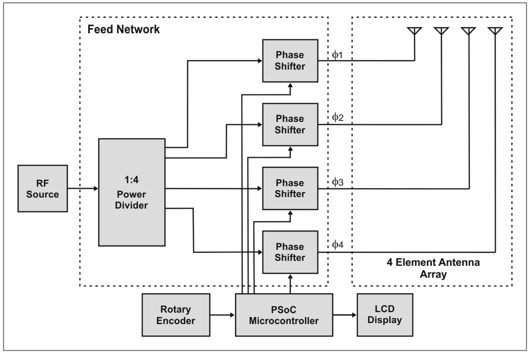
Fig. 1. Design configuration of the proposed system to generate progressive phase shifts.
Power divider design and working principle
Power divider which forms the first block of the overall structure plays an important role in directing the beam to the phase shifters connected across its output ports. Feeding network to the final array antennas is carried out by amalgamation of power divider and phase shift network. The corporate and series feed techniques are used for feeding the antenna arrays where single/multiple TLs are used for feeding the series/corporate network. Fabrication of series feed network is easier however high voltage standing wave ratio (VSWR) due to additive mismatch and progressive phase delay makes it unsuitable for such application. Corporate feed network on the other side offers great flexibility and better control of phase for each array. Individual excitation to array elements with equal power divider and line lengths is supplied by corporate feed.
Figure 2 shows the proposed 1:4 WPD which plays a significant role in communication systems because of its characteristics namely, simple configuration, matching of impedance, and isolation at output ports. The structure of the WPD, as shown in Fig. 2, comprises two λ/4 TLs at a resonating frequency of 2.45 GHz and the branch impedances $\sqrt {2Z_0}$ and 2Z 0. The circuit is analyzed using an even–odd mode analysis [Reference Nikfalazar, Sazegar, Mehmood, Wiens, Friederich, Maune, Binder and Jakoby22, Reference Yang, Cao, Gao, Yang and Li23]. The 100 Ω resistors used at the output ports enable the output to match at the same time also ensure better isolation. The fabricated power divider is depicted in Fig. 3 which is printed on the FR-4 substrate (εr: 4.3, thickness: 1.6 mm) having an overall dimension of 157 × 112 mm2. The WPD acts as a network of corporate feed for feeding the phase shifter with equal phase and amplitude. The output ports have no reflection and hence, they are perfectly isolated.

Fig. 2. Schematic geometry of 1:4 Wilkinson power divider (WPD).

Fig. 3. Fabricated prototype of 1:4 WPD.
To comprehend the working principle, the surface current distribution of power divider at 2.45 GHz is shown in Fig. 4 where it can be observed that no coupling current is present between ports when port 1 is excited by terminating the other ports and observing the current at the testing port (shown with dotted red line). Further to validate the current distribution when port 2, 3, 4, and 5 are excited, it is observed that the current flows through the designated path only (shown with red-dotted line) in Figs 4(b)–4(e), respectively.

Fig. 4. Surface current at (a) port 1, (b) port 2, (c) port 3, (d) port 4, and (e) port 5.
Figure 5 illustrates that the power divider has a measured fractional bandwidth of 39.69%. It can also be visualized that the measured S 21, S 31, S 41, and S 51 are −6.25, −6.31, −6.28, and −6.31 dB, respectively, which are very low and shows good agreement with the simulated values. It can also be seen that, S 21, resembles S 31, S 41, and S 51 which indicates that the power has been distributed equally to all the output ports.

Fig. 5. S-Parameters result of the WPD: (a) S 11, (b) S 21, (c) S 31, (d) S 41, and (e) S 51.
From the above analysis, it can be verified that the designed 1:4 power divider shows good performance as it has low insertion loss and good VSWR.
Phase shifter design and working principle
The phase shifter is implemented using an analog variable control voltage IC 2484. The chip is mounted on TB-122B authorized layout printed circuit board (PCB) with internal view as shown in Fig. 6. It is built on a test panel that utilizes grounded co-planar waveguides for input–output RF excitation. The substrate used in the test board PCB is Rogger-R0 4350 with a dielectric constant of 3.5 and a thickness of 0.762 mm. All traces on the test board are made with electrolysis nickel using 1 oz of copper. In order to allow measurements, female sub-miniature version (SMA) connectors are used at both the input and output RF ports.

Fig. 6. Phase shifter: (a) top view and (b) inner view.
The four-phase shifter ICs as shown in Fig. 7A are connected in the system layout such that the RF input given to 1:4 WPD equally divides the amplitude and phase and provides the same input to each of the phase shifters. The control voltage from the power supply 0–15 V is regulated through a control switch and is applied to each control pin 6 of the IC 2484. The control voltage is varied in the step of 0.5 V and a set of readings for each individual phase shifter are taken and stored in the look-up table.

Fig. 7. (A) Block diagram for calibration a phase angle versus control voltage. (B) Variation of phase shift with voltage of (a) phase shifter 1, (b) phase shifter 2, (c) phase shifter 3, and (d) phase shifter 4.
The graphs plotted in Figs 7B(a)–7B(d) show the variation of the control voltage versus progressive phase shift. It can be observed from IC 2484 datasheet that the individual phase shifter always shows a positive phase angle when the voltage is varied from 0 to 15 V. However, when phase shifters are used as a feed network, they are supposed to give a progressive phase shift to form a beam in the phased-array antenna. The plotted data confirm that the phase shifters yield both positive and negative phase angles leading to generate progressive phase shift when connected in the system. The phase shift data are stored in the look-up table for further processing with the PSoC controller.
According to the datasheet of IC 2484, VSWR varies from 1.5 to 2 and the reflection coefficient (S 11) less than −10 dB is expected. The S 11 (dB) and VSWR value below −10 dB and 1.58, respectively, are achieved for the band of interest as shown in Figs 8(a) and 8(b), respectively.

Fig. 8. Frequency versus S 11 and VSWR of phase shifter: (a) S 11 (dB) and (b) VSWR.
To verify the impact of interfacing WPD with phase shifter, the insertion loss is shown in Figs 9(a)–9(d) from ports 2 to 5. It is visualized that the insertion loss from ports 2 to 5 is −8.21, −8.32, −8.29, and −8.39 dB, respectively. These variations may be due to a fabricated power divider and soldering of SMA connectors. After deducting the insertion loss due to the power divider, the net insertion losses that occur due to the phase shifter at ports 2, 3, 4, and 5 are −1.73, −1.88, −1.78, and −1.84 dB, respectively. The average value of the insertion loss is −1.80 dB, which is well within the specified value of 5.6 dB [Reference Hosseinnezhad, Nourinia and Ghobadi26].

Fig. 9. Insertion loss of WPD with phase shifter IC 2484: (a) S 21, (b) S 31, (c) S 41, and (d) S 51.
Antenna design and working principle
Figure 10 illustrates the schematic geometry of antenna having dimensions of 90 × 96 mm2. The antenna consists of an inverted L-shaped dipole on the front as shown in Fig. 10(a) and two mirrored inverted L-shaped dipoles mounted on a rectangular conductive structure on the back as depicted in Fig. 10(b). Via is inserted on the left inverted L-shaped dipole on the back which helps in enhancing the bandwidth. Vias are also incorporated near the feed which helps in getting directive patterns and leads to lowering of back radiation as suggested in [Reference Kulkarni, Kulkarni and Desai27].

Fig. 10. Antenna geometry: (a) top view and (b) back view.
The antenna ground plane evolution in terms of S 11 from steps 1 to 5 (proposed antenna) design is depicted in Fig. 11. It is observed that by inserting the mirrored inverted L-shaped conductive structures with thick bottom interfaced over a truncated rectangular block from both sides and inserting via helps in substantial bandwidth enhancement spanning from 2.09 to 3.10 GHz.

Fig. 11. Antenna ground plane evolution.
An FR4 substrate (tan δ = 0.02, εr = 4.4) having a thickness of 1.6 mm is used for realizing the dipole antenna. The design parameters of dipole antenna are indicated in Fig. 10 which is achieved after optimizing the antenna dimensions and carrying out the performance analysis in terms of reflection coefficient. The fabricated dipole antenna is illustrated in Figs 12(a) and 12(b).

Fig. 12. Fabricated antenna geometry: (a) top view and (b) back view.
In order to validate the simulation results, a vector network analyzer Rohde & Schwarz (9 kHz to 13.6 GHZ) is used to measure reflection coefficient S 11 (dB) characteristics and VSWR, while gain and radiation patterns are measured using an anechoic chamber.
Figure 13 shows that the simulated and measured S 11 curves are matching well with each other. A minimal deviation is found, which may be due to cable losses while used at the time of measurement, and fabrication tolerances. From Fig. 13, it is visualized that the proposed dipole antenna design exhibits the measured fractional impedance bandwidth of 39.69% (2.08–3.11 GHz) to function smoothly in ISM/Wi-Fi frequency bands.

Fig. 13. Reflection coefficient S 11 (dB) versus frequency (GHz) curves.
To verify the range of broadcasting station, nulls, azimuth, and attenuation, the radiation patterns of the proposed dipole antenna in the E-plane (YZ), $\phi = 0^\circ$ and H-plane (XZ), $\phi = 90^\circ {\rm \;}$
 at 2.45 GHz are depicted in Fig. 14. It is apparent that in the E-plane, main lobe magnitude of 5.52 dB is achieved in the 90° direction with minimum side lobe of magnitude of −10.6 dB. In the H-plane, dipole patterns (figure of eight shape) are observed with main lobe magnitude of around 1 dB indicating an omni-directional radiation with dominant null radiations occurring at an angle of 90°.

Fig. 14. Radiation patterns at 2.45 GHz: (a) E-plane and (b) H-plane.
Figure 15 illustrates that the proposed dipole antenna radiates with an efficiency of >78% with gain closer to 5 dBi throughout the operating band (2.08–3.11 GHz). The gain and efficiency are calculated using the formula mentioned in [Reference Ji, Ge, Wang, Chen, Wu and Li20]. It can also be visualized that there is minimum deviation between the simulated and measured results which may be due to fabrication tolerances.

Fig. 15. Gain and efficiency.
Therefore, from the analysis and measurement of scattering and radiation performances, it is confirmed that the proposed antenna is a good candidate for ISM/Wi-Fi applications and it can be easily integrated with the programmable phase shifter.
Proposed system design using PSoC
A proposed system is implemented using a combination of both custom hardware and PSoC processor to reconfigure analog and digital blocks in a real-time environment that permits the design to perform more than one function or adopt to perform better. The PSoC is used as a data acquisition and as beamforming controlling tool for higher sampling/conversion rate, to detect smaller change that can easily represent.
The 1 × 4 antenna array is constructed with a feed network that includes an RF source and a 1:4 power divider with the voltage controlled analog phase shifter IC. The array system was implemented for 2.45 GHz, four-element linear antenna array. The RF signal of 2.45 GHz is given as an input to the power divider. The power divider provides the same signal to the phase shifters. The block diagram of the proposed system for implementation and analysis using PSoC is shown in Fig. 1. Progressive phase shifts are controlled by PSoC for electronic beamforming.
As per the direction of arrival estimation, PSoC read and determine rotary encoder position and direction which provides the required biasing voltage for phase shifters and set progressive phase shifts for phased-array antenna elements. A beamforming system is developed using PSoC, which provides the optimal balance between performance and development time.
Block diagram of PSoC creator IDE
Programing a PSoC is a combination of drag and drop components and wiring and programing in C code. Following component icons such as IDAC, Character LCD, GPIO, and MUX are used for an embedding PSoC Creator IDE for the proposed system. Figure 16 shows the block diagram that provides a detailed execution of the program to set the control voltage for the phase shifter IC 2484 through the PSoC and generate progressive phase shifts for the 1 × 4 phased array.

Fig. 16. Block diagram to set control voltage to generate progressive phase shift using PSoC 4 Creator IDE.
Flowchart of PSoC
The flowchart in Fig. 17 shows the step-by-step execution of PSoC, integrated development environment (IDE). The flowchart which gives step by step execution to write the program for PSoC creator IDE is shown in Fig. 16.

Fig. 17. Flowchart for PSoC Creator IDE.
Progressive phase shifts are controlled by PSoC for electronic beamforming. Both numerical and empirical investigations are undertaken to measure performance. In the real-time environment when it comes in linking the RF components with software is always been one of the biggest challenges as it requires an understanding of RF-specific concepts which demand more attention for proper tuning than convectional circuit design, facing difficulties in adapting new environment, cope up to meet required new functionalities, ensuring smooth integration, consumes low power, testing and operating speed. This study is one of the first to demonstrate beamforming using PSoC which operates at 2.45 GHz frequency. In this proposed system, we successfully embed both RF component and PSoC controller together in such way that control voltages set for each phase shifter will generate the beam pattern that is directive and steered successfully with great cross polarization level (XPD level). It is noted that in the proposed system, speed of excitation of phases are not affected the beam performance and the progressive phase shift obtained within ±5% accuracy which is used to steer the beam in the desired direction. Results show that the proposed method provides a good estimation of relative system performance, which can be useful as a criterion choice for selecting the PSoC-embedded platform. After building the program in the PSoC processor, it works freely at the site of work for controlling or for detecting some input.
Simulated and measured phased-array antenna
Furthermore, the entire system is designed and simulated using CST software to observe the performance when used in a 1 × 4 antenna array. Depending upon the control voltage set by the PSoC, $s_p^2$ files of IC 2484, the progressive phase shifts are generated which is provided to the 1 × 4 phased array. A schematic view of the simulated phased-array antenna using a $s_p^2$
 file of IC 2484 is displayed in Fig. 18.

Fig. 18. Simulated schematic view of phased-array antenna with $s_p^2$ file of IC 2484.
To validate the progressive beam patterns, the phased-array antenna system is assembled as shown in Fig. 19 along with subsystem components such as WPD, phase shifter, a controlled circuit using PSoC, and four-element antenna arrays along with an Antenna Measurement System CISPER 1-1-1.
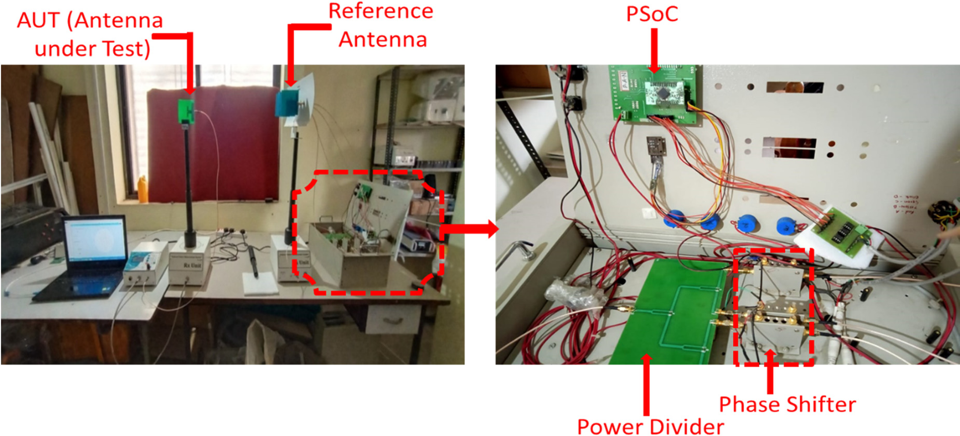
Fig. 19. Experimental set up for the validation of the programmable phase shifter.
The radiation patterns for different scan angles of 30, 60°, and 90° are plotted in Figs 20(a)–20(c) for experimental and simulated phased-array antennas. From Figs 20(a)–20(c), it is visualized that the simulated and measured beam patterns match accurately which clearly shows the correctness of control circuit designed using PSoC.

Fig. 20. Simulated and measured radiation beam patterns at (a) 30°, (b) 60°, and (c) 90°.
Moreover, it is also observed that the gain degradation in the measured results may be due to losses in the feed network, cables, and connectors used in the experimental setup. The average simulated and measured gain is 13.48 and 13.03 dBi, respectively in the operating band. It is observed that the experimental gain is less than the simulated gain by 0.45 dBi. The level of the side lobe discrepancies may be due to the infinite ground plane assumed in the simulation and the finite ground plane used in the fabricated array. However, SLL is maintained below −13 dB in both the cases. This shows that the accuracy of calibration of progressive phase angles is within limits.
Performance comparison of proposed design
Table 1 shows the comparison of the proposed design with the existing state-of-the-art in terms of power distribution, operating frequency, number of output ports, and design process of phase shifters, insertion loss, and gain of complete system.
Table 1. Performance comparison of various types of reported phase shifters

From Table 1, it can be observed that the designed four-output power divider is uniform in nature and operates at the 2.45 GHz band. The designed phase shifter is simple and it uses an innovative PSoC technique to generate beam patterns at the desired phase angles. The complete design has low insertion loss and VSWR. The system has a high gain >13 dB in the operating band.
Conclusion
In this study, a phased-array antenna realized using a dipole antenna as the basic element combined with the power divider and PSoC-based phase shifter is proposed. Dipole antenna covers IBW of 39.69% with directional radiation patterns. Measured S 21, S 31, S 41, and S 51 are −6.25, −6.31, −6.28, and−6.31 dB, respectively, for power the divider which are very low and shows good agreement with the simulated values. A high-performance analog phase shifter using IC 2484 is analyzed, simulated, calibrated, and tested at an ISM band. The phase shifter has low variation in the insertion loss which leads to successful transmission in the linear array antenna. After deducting the insertion loss due to the power divider, the net insertion losses that occur due to the phase shifter at ports 2, 3, 4, and 5 are −1.73, −1.88, −1.78, and −1.84 dB, respectively. The average value of the insertion loss is −1.80 dB which is well within the specified value of 5.6 dB. The radiation patterns for different scan angles of 30, 60, and 90° are plotted for phased-array antenna where simulated and measured beam patterns match accurately which clearly shows the correctness of the control circuit designed using PSoC.
 Aparna Balaji Barbadekar has been working as assistant professor in the Department of Electronics and Telecommunication Engineering at Vishwakarma Institute of Information Technology, Pune, till date. She has received good and steady support from her parent institute and her guide.
 Dr. Pradeep Mitharam Patil who is presently working as principal, SND College of Engineering and Research Center, Yeola District, Nashik, Maharashtra, India. He is member of various professional bodies such as IE, ISTE, IEEE, and Fellow of IETE. He has been recognized as a PhD guide by various Indian universities such as the University of Pune, Shivaji University, Kolhapur, and North Maharashtra University, Jalgaon. His research areas include pattern recognition, neural networks, fuzzy neural networks, and power electronics.


