1. INTRODUCTION
There has been a continued interest in explosive emission cathode that can be used in the generation of high-current electron beams driving high-power microwave (HPM) sources (Eltchaninov et al., Reference Eltchaninov, Korovin, Rostov, Pegel, Mesyats, Rukin, Shpak, Yalandin and Ginzburg2003; Korovin et al., Reference Korovin, Kurkan, Loginov, Pegel, Polevin, Volkov and Zherlitsyn2003; Mesyats et al., Reference Mesyats, Korovin, Gunin, Gubanov, Stepchenko, Grishin, Landl and Alekseenko2003; Barker et al., Reference Barker, Booske, Luhmann and Nusinovich2005; Benford et al., Reference Benford, Swegle and Schamiloglu2007). The explosive process leads to the formation of a plasma sheath on the cathode surface, from which a space-charge limited electron flow can be extracted by an externally applied electrical field (Bugaev et al., Reference Bugaev, Litvinov, Mesyats and Proskurovskii1975; Litvinov, Reference Litvinov1985; Miller, Reference Miller1998). Historically, velvet fabric was considered as one of the best materials for manufacturing cold cathodes due to its ability to generate high uniform plasma across a larger area (Hegeler et al., Reference Hegeler, Friedman, Myers, Sethian and Swanekamp2002; Yang et al., Reference Yang, Shu and Wang2012a, Reference Yang, Shu, Zhang, Fan and Zhub, Reference Yang, Shu, Zhang and Fan2013a, Reference Yang, Shu, Zhang and Fanb). This kind of material has been widely used in a variety of HPM devices, such as magnetically insulated transmission line oscillator (MILO) (Fan et al., Reference Fan, Yuan, Zhong, Shu, Zhang, Yang, Yang, Wang and Luo2008a, Reference Fan, Zhong, Li, Shu, Yang, Zhou, Yuan, Zhou and Luob, Reference Fan, Zhong, Li, Yuan, Shu, Yang, Wang and Luo2011), and magnetron (Saveliev et al., Reference Saveliev, Kerr, Harbour, Douglas and Sibbett2002). Usually, the HPM devices suffer from impedance collapse and cathode material degradation or even failure. Generally, these problems are attributed to the characteristics of cathode material such as the expansion of cathode plasma and ablative performance. In fact, when the intense electron beam hits the anode (or named as collector in HPM device), an anode plasma could appear under certain conditions. In this case, the impedance collapse is caused by the expansions of the cathode and anode plasmas. As a result, the diode current rises suddenly due to the bipolar flow.
The anode plasma can be generated by either melting and subsequent evaporation of the anode material or by an electron stimulated desorption of the contaminants on the anode surface (Saveliev et al., Reference Saveliev, Sibbett and Parkes2003). The former is unlikely under moderate energy fluxes in previous experiments operated in the air force research laboratory of USA. The results imply that contaminants in the anode, in the bulk of the materials and on the surface, lead to bipolar flow in the diode. The bipolar flow can be initiated on very short time scale, on the order of 10 ns. It is evident at beam power densities of 2 MW/cm2 and the pulse durations of 50 ns (Shiffler et al., Reference Shiffler, Ruebush, Haworth, Umstattd, Lacour, Golby, Zagar and Knowles2002a, Reference Shiffler, Ruebush, Zagar, Lacour, Sena, Golby, Haworth and Umstattdb, Reference Shiffler, Luginsland, Umstattd, Lacour, Golby, Haworth, Ruebush, Zagar, Gibbs and Spencerc). However, other experiments indicated that the charged particle flow in the diode is unipolar at moderate diode voltages <170 kV, when the electron current density does not exceed 16 A/cm2 and beam power densities is less than 2 MW/cm2 with pulse durations of ~2 µs. The bipolar flow was only achieved, when an arrangement was made to ensure a fast generation of dense plasma on the anode (Saveliev et al., Reference Saveliev, Sibbett and Parkes2003).
Furthermore, irradiation with the high-power pulsed electron beam gives rise to deformation, erosion, and changes in the microscopic structure of the anode surface (Li et al., Reference Li, Liu, Cheng, Xu, Ge and Wen2009, Reference Li, Liu, Zhang, Wen, Wan and Chu2014) consequently affecting the operation of the diode.
In this paper, we begin with investigating a possibility of the bipolar flow development in planar explosive emission diodes at moderate energy fluxes. And then, based on the analysis of the thermal region of the anode irradiated with the high-power pulsed electron beam, the preliminary generation mechanism of the bipolar flow is obtained. Next we discuss the diode performance, which is influenced by the expansion of the cathode and anode plasma as well as by the anode damage (erosion).
2. EXPERIMENTAL SETUP AND DIAGNOSTICS
These experiments took place on a high-voltage nanosecond electron modulator platform. The pulser schematic is shown in Figure 1. The adjustable output voltage of the modulator ranged from 200 to 500 kV, with pulse rise-time (10–90% amplitude) of 25 ns and pulse duration [full width at half maximum (FWHM)] of ~110 ns. A primary capacitor is charged to a maximum voltage of 28 kV and then switched through the primary of a 19:1 setup charging transformer. The secondary of the transformer charge a spiral coaxial pulse forming line (PFL). The PFL is switched to a spiral transmission line using a gas switch which can be filled either with nitrogen (N2) or sulfur hexafluoride (SF6). This particular design where an additional spiral delay line was added to a coaxial line, helped to realize the accurate synchronization between the exposure time of camera and the luminescence process of diode plasmas. The high voltage pulse was delivered to the cathode after the spiral transmission line. The vacuum vessel operated with base pressures of 2~5 × 10⁻⁵ Torr, utilizing a turbo-molecular pump backed by an oil roughing pump.

Fig. 1. Schematic diagram of experimental setup.
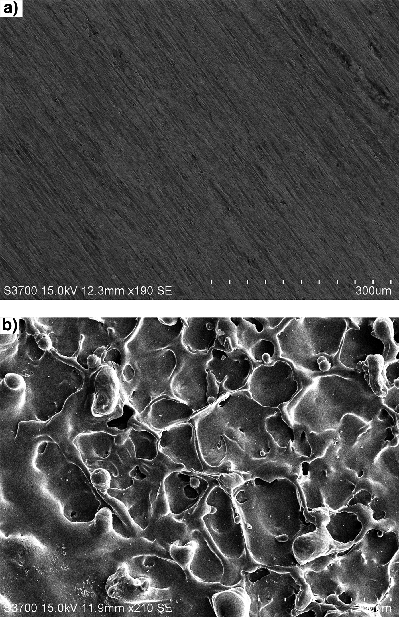
The cathode holder had a 6-cm diameter and was recessed by ~2 mm with respect to the surrounding cathode electrode (see Fig. 2a). The velvet sample in the experiments comes from the existing material used in a MILO tube (Fan et al., Reference Fan, Yuan, Zhong, Shu, Zhang, Yang, Yang, Wang and Luo2008a). The area of the velvet cathode was about 28.3 cm2, and it was glued on a stainless steel substrate. Figure 2 shows the structure of unused velvet cathode and its morphological characterization and composition. Morphological characterization and composition change of the velvet cathode and anode plate were measured with scanning electron microscope (SEM) and X-ray energy dispersive spectroscopy (XEDS). Figure 2b shows that the velvet fibers consisting of series of randomly oriented tips can emit with a relatively uniform electron beam at a low turn-on field. The cathode composes of 7~10 µm diameter velvet fibers. The surface morphology of fiber resembles with each other and is almost smooth at an amplification of 600. The local surface of velvet cathode is analyzed by XEDS to acquire the composition data before operation under high externally applied electrical field electron beam and the results are shown in Figure 2c. From the energy spectrum and composition data unlisted here, the velvet fibers are composed of C, O. The C concentration is 27.29%.
Fig. 2. (a) Fresh polymer velvet cathode, (b) SEM image of polymer velvet before the interaction with pulsed electron beam, and (c) XEDS of fresh polymer velvet.
Normally, the anode was positioned at a distance between A and K gaps ranging from 15 to 40 mm. In the experiments, the anode was carefully treated before being placed under vacuum. First, it was sanded to the desired surface finish. Then, it was cleaned with denatured alcohol and then wiped with a clean tissue. A viewing port was located axially along the A–K gap such that the entire A–K gap, including both cathode and anode, can be imaged.
The diode voltage and anode current were, respectively, measured using a resistive divider and Rogowski coil. The Rogowski coil is located at the anode holder, therefore the current is the sum of electronic current and ionic current. Due to the ratio of the electron mass to ion mass is very small, the electronic current is much bigger than the ionic current. The High Speed Framing Camera (HSFC) with four microchannel plates image intensifier modules was used to observe the light emission from diode plasma. The spectral response of HSFC is 280~1000 nm. In order to avoid the reflection light, the inner surface of the vacuum chamber has been covered by some low-reflectivity material (Cai et al., Reference Cai, Liu, Ju, Zhao and Qiu2014).
3. RESULTS AND DISCUSSIONS
3.1. General characteristics of the diode operated in a bipolar flow mode
The typical diode voltage and current from the modulator (with all cable delays taken into account) at A–K gap d ac = 30 mm are shown in Figure 3 for a stainless steel anode of 75 mm radius. The diode voltage could be increased by altering the pressure of the gas switch. Figure 3a presents the diode operated at the gas switch filled with 1 atm nitrogen. The polymer velvet cathode was fired at 211 kV and 0.69 kA. The initial turn on of the diode current occurred when the typical macroscopic field was 60 kV/cm at ~30 ns after the start of the voltage pulse. Corresponding to the experimental data, the current predicted for pure electron Child-Langmuir flow was 0.71 kA (Child, Reference Child1911; Langmuir, Reference Langmuir1911). This indicates that the polymer velvet cathode operated at electron space-charge limited flow. The diode current waveform has a 60 ns flattop form 38 ns during the flattop of diode voltage. The diode voltage was raised up to 301 kV by increasing the pressure in the gas switch (see Fig. 3b). It was shown that the major difference lays in the current waveform during the flattop of diode voltage. Before T 2 = 63 ns, the diode operated normally as shown in Figure 3a. The onset turn on of the diode current occurred when the typical macroscopic field was 65 kV/cm at T 0 = 11 ns. The amplitude of the current increased with the voltage pulse until reaching the first current flattop at T 1 = 32 ns. The current almost remain unchanged with amplitude of 1.2 kA which is equal to the theoretical value expected, based on Child-Langmuir electron space-charge limited flow during the first current flattop. From T 2 = 63 ns to T 3 = 95 ns (refer to the end of the flattop of voltage), the amplitude of current shots up to 2.35 kA which is 1.96 times the pure electron space-charge limited unipolar flow.
Fig. 3. Typical waveforms with different accelerating voltage (a) 211 kV, (b) 301 kV.
The current rise during the flattop of voltage could be attributed to two main reasons: The expansion of plasma (form nearby the surface of cathode and anode) and the effect of bipolar flow. Regarding the common cathode materials such as graphite, polymer velvet, and stainless steel (SS) anode, the total expansion velocity of cathode and anode plasma is less than 11 cm/μs (Roy et al., Reference Roy, Menon, Mitra, Mitra, Kumar, Sharma, Nagesh, Mittal and Chakravarthy2009). The decrease of A–K gap is less than 0.4 mm during the time interval of current shot up (less than 32 ns). The effect of plasma expansion could be ignored for the A–K gap of 30 mm. For space-charge-limited bipolar flow, the ionic current is  $\sqrt {{{{m_{e}}} / {{m_{i}}}}} $ times the electron current, where m e is the electron mass and m i is the ion mass. The charge neutralizations of the electrons by the ions allow ~1.86 times the current to flow compared with single species Child-Langmuir with the limiting electron current independent of the ion mass (Miller, Reference Miller1982). It is the possible reason for the peak current is slightly more than 1.86 times the pure electron space-charge limited unipolar flow that decrease of A–K gap caused by the axial expansion of plasma and the increase of effect electron emission area is caused by the radial expansion of cathode plasma.
The profiles of the typical plasma image are shown in Figure 4. The anode appears on the right and the cathode on the left. The A–K gap was 30 mm with aluminum anode. The image was registered with a frame duration of 120 ns. The anode plasma is clearly visible in the image which appears in the central area of the anode plate. The radial and axial expansions of cathode plasma indeed change the actual structure of diode (effective emission area and A–K gap). More accurate and quantitative information about the expansion of diode plasmas was obtained by utilizing digital images methods (Yang et al., Reference Yang, Shu, Zhang and Fan2012aReference Yang, Shu, Zhang and Fanb; Cai et al., Reference Cai, Liu, Ju, Zhao and Qiu2014). The decrease of A–K gap is less than 5 mm during 120 ns. All of this confirms the analysis about the reason why the peak current is slightly more than 1.86 times the pure electron space-charge limited unipolar flow.
Fig. 4. Typical side images of the light emission from the diode with anode plasma.
3.2. The thermal regime of the anode
The issue is the generation mechanism of ions for the bipolar flow. These ions must originate from the anode plasma. The anode plasma could be generated by either melting and subsequent evaporation of the anode material or by an electron stimulated or thermal desorption of the contaminants on the anode surface (Cuneo et al., Reference Cuneo, Menge, Hanson, Floler, Bernard, Ziska, Filuk, Pointon, Vesey, Welch, Bailey, Desjarlais, Lockner, Mehlhorn, Slutz and Stark1997; Cuneo, Reference Cuneo1999; Shiffler et al., Reference Shiffler, Luginsland, Umstattd, Lacour, Golby, Haworth, Ruebush, Zagar, Gibbs and Spencer2002c; Saveliev et al., Reference Saveliev, Sibbett and Parkes2003). The generation mechanism of the anode plasma can be deduced by analyzing the thermal regime of the anode, which is impacted by the high-power electron beams. In order to simplify the analysis, the anode plasma generation time T P is defined as the difference between T 2 and T 0. Here, T P is 52 ns.
Firstly, the dose of the onset of anode plasma is calculated with a numerical method. The particle in cell code KARAT (Tarakanov, Reference Tarakanov1992) was employed to simulate the diode performance. Figure 5 shows the typical phase-space picture of electrons with the A–K gap of 30 mm and diode voltage of 301 kV. With the absence of an external guiding magnetic field, the radius of electron beams expands from 30 to 32 mm due to its own space charge. In other words, the effective impact area S eff on the surface of anode plate is 32 cm2.
Fig. 5. Typical phase-space picture of electrons by using particle in cell (PIC) code KARAT.
Figure 6 presents the power and energy densities of electron beam deposited on the SS plate as a function of time. At the moment T = T 2, the total pulse energy density ρE on the SS anode plate is 0.485 J/cm2.
Fig. 6. Beam power and energy deposition density.
In this paper, a Monte Carlo simulation code (CASINO V2.4) (Drouin et al., Reference Drouin, Couture, Joly, Tastet, Aimez and Gauvin2007) was utilized to simulate the electron trajectory in the SS anode plate. As we know, the deposition depth of electron beams is relative to the incidence angle Therefore, it is necessary to obtain the distribution of incident angle before the simulation of the movement of electrons in the anode plate. The relationship between the ratio P r/P z (stand for the ratio of radial component and axial component of the incident electron beams moment) and radial position on the surface of anode plate R are shown in Figure 7. The data of Figure 7 was obtained from the phase space picture of the incidence electron beams nearby the anode plate during the flattop of voltage. The maximum of the ratio is 0.11, which means the incident angle of electron beams is larger than 84°.That is to say the electron beams almost vertically impacts on the surface of anode plate.
Fig. 7. The relationship between ratio P r/P z and radial position on the surface of anode plate R.
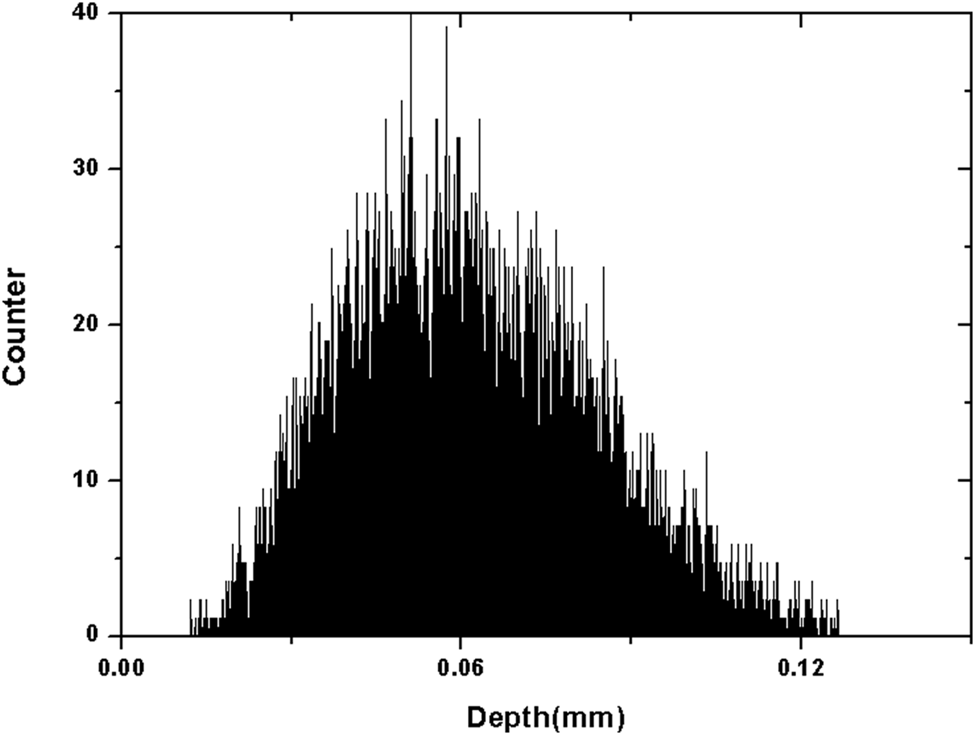
The distribution of number of electrons stopped as a function of the deposition depth is shown in Figure 8. The total number of incident electron is 10 000 with energy of 301 keV. The composition of the SS anode plate is set in the CASION V2.4 as C, Si, Mn, P, S, Cr, Ni, and Fe (refer to SS 304L). The concentration (wt.%) of Fe and Cr is 68.855 and 19%, respectively, and that of Ni is 9%. The maximum deposition depth D max is 0.13 mm when the electron beams vertically impact on the anode plate. The relationship between the stop electron number and the deposition depth appear approximately a normal distribution.
Fig. 8. Number of deposit electrons versus the deposition depth with the electron energy 301 keV and SS anode.
It is necessary to consider the relation between the maximum deposition depth and the penetration depth of the temperature field before calculating the dose of the onset of anode plasma. The penetration depth of the temperature field could be expressed as (Mesyats, Reference Mesyats2000):
 $${R^{\prime}} = \sqrt {\displaystyle{{\lambda {T_{\rm P}}} \over {{\rm \rho} c}}} $$
Here, λ is the heat conductivity, ρ is the density, c is the specific heat, and T p is the anode plasma generation time. In this case, T p = 52 ns, λ = 1.62 W/cm, ρ = 8 g/cm3, and c = 0.5 J/g °C for the SS anode. The penetration depth of the temperature field R′ is about 1.45 × 10⁻³ mm (Yang, Reference Yang2013).
The heat release in the anode bulk can be neglected for R′ ≪ D max, therefore, the dose of the onset of anode plasma is:
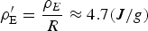 $${\rm \rho}_{\rm E}^{\prime} = \displaystyle{{{\rm \rho}_E} \over R} \approx 4.7(J/g)$$
The total electron energy density incident in the anode or anode dose is well below that is required for direct vaporization or change of state. According to the calculations, the melting threshold of SS 304L is achieved at ρE = 2~2.5 J/cm2 or ρ′E = 19~25 J/g (Zecca et al., Reference Zecca, Brusa, Naia, Paridaens, Pogrebnjak, Markov, Ozur, Proskurovsky and Rotstein1993; Markov & Rotstein, Reference Markov and Rotstein1997). The anode plasma could not be generated by melting and subsequent evaporation of the anode material in this case.
Stimulated desorption is important in the initiation of events on anode at low temperature, under special conditions with high current density or avalanches of low energy (1–1000 eV) electron, and also with particular contaminants with the high elastic cross-section (Halbritter, Reference Halbritter1982, Reference Halbritter1983, Reference Halbritter1985, Reference Halbritter1986). The thermal desorption of the contaminants could dominate the desorption with elevated anode temperatures >300°C (Cuneo, Reference Cuneo1999). Whether the electron stimulated desorption or thermal desorption of the contaminants is important in the generation of the anode plasma depends on the thermal regime of the anode under impacting by the high-power electron beams.
Since thermal conduction losses can be neglected on a 50 ns time scale (Cuneo et al., Reference Cuneo, Menge, Hanson, Floler, Bernard, Ziska, Filuk, Pointon, Vesey, Welch, Bailey, Desjarlais, Lockner, Mehlhorn, Slutz and Stark1997), the average of anode temperature rise can be estimated as follows:
 $$\Delta T(t) = \displaystyle{1 \over {{\rm \rho} c}}\int\limits_{{T_{P}}} {\displaystyle{{V(t)J(t)dt} \over {{Z_{\max}} (V,{\rm \theta} )}}} $$
where V(t) is the diode voltage, J(t) is the current density, Z max(V, θ) is the maximum deposition depth as the function of electron energy and incident angle. While the Z max(V, θ) could be reasonably simplified as a constant value of 0.13 mm, and then the eq. (3) could be rewritten as follows:
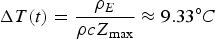 $$\Delta T(t) = \displaystyle{{{{\rm \rho}_E}} \over {{\rm \rho} c{Z_{\max }}}} \approx {9.33^{\circ}}C $$
This means the electron stimulated desorption played the most important role in the generation of anode plasma in this case. The result could also be confirmed in the other experiment (Shiffler et al., Reference Shiffler, Luginsland, Umstattd, Lacour, Golby, Haworth, Ruebush, Zagar, Gibbs and Spencer2002c).
The above analysis assumed a uniform energy loss to characterize the penetration process of the electron beams. In fact, the response of solid material under the impact of electron beams is quite complex. In addition, only about 90% losing energy of incident electron could be translated to heat the material. The other is carved up to generate the backscattered electron, secondary electron, X-ray, and Cherenkov radiation, etc.
The more realistic analysis is carried out as follows. The penetration process of the electron on the anode is instantly completed. In addition, the whole diode is in a high vacuum environment. The effect of the heat convection and heat radiation could be reasonably ignored in this case. A one-dimensional heat equation for the z axis directed perpendicular to the anode surface can be described as:
 $${\rm \rho} c\displaystyle{{{\rm \partial} T} \over {{\rm \partial} t}} = \displaystyle{{\rm \partial} \over {{\rm \partial} z}}\left( {{\rm \lambda} \displaystyle{{{\rm \partial} T} \over {{\rm \partial} z}}} \right) + W(z,t)$$
Here, W(z,t) is the absorbed energy per unit volume by electron-beam irradiation, which could be given as:
 $$W(z,t) = {{\rm \eta} _{A}}P(t)f(z)$$
Here, ηA is the conversion ratio (~90%), P(t) is the power density of the electron flow, f(z) is the distribution of energy deposition with the penetration depth.
In order to simplify the simulation, the relationship between P(t) and the generation time of anode plasma could be treated as a right trapezoid approximately. The rising rate of power density  ${\dot P_1}$ is calculated to be
 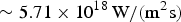 $\sim 5.71 \times {10^{18}}\,{\rm W}/({{\rm m}^2}{\rm s})$ during the time interval from T 0 to T 1. The power density P 2 during the flattop is 1.2 × 10¹¹ W/m2. Furthermore, the power density could be expressed as:
 $$P(t) = \left\{ {\matrix{ {{{\dot P}_1}t{\kern 1pt} {\kern 1pt} {\kern 1pt} {\kern 1pt} {\kern 1pt} {\kern 1pt} {\kern 1pt} {\kern 1pt} {\kern 1pt} {\kern 1pt} {\kern 1pt} {\kern 1pt} {\kern 1pt} {\kern 1pt} {\kern 1pt} {\kern 1pt} {\kern 1pt} {\kern 1pt} {\kern 1pt} {\kern 1pt} {\kern 1pt} {\kern 1pt} {\kern 1pt} {\kern 1pt} {\kern 1pt} {\kern 1pt} {\kern 1pt} {\kern 1pt} {\kern 1pt} {\kern 1pt} {\kern 1pt} {\kern 1pt} {\kern 1pt} {\kern 1pt} {\kern 1pt} {T_0} \lt t \lt {T_1}{\kern 1pt} {\kern 1pt}} \cr {{P_2}{\kern 1pt} {\kern 1pt} {\kern 1pt} {\kern 1pt} {\kern 1pt} {\kern 1pt} {\kern 1pt} {\kern 1pt} {\kern 1pt} {\kern 1pt} {\kern 1pt} {\kern 1pt} {\kern 1pt} {\kern 1pt} {\kern 1pt} {\kern 1pt} {\kern 1pt} {\kern 1pt} {\kern 1pt} {\kern 1pt} {\kern 1pt} {\kern 1pt} {\kern 1pt} {\kern 1pt} {T_1} \le t \lt {T_{2{\kern 1pt}}} {\kern 1pt}} \cr}} \right.$$
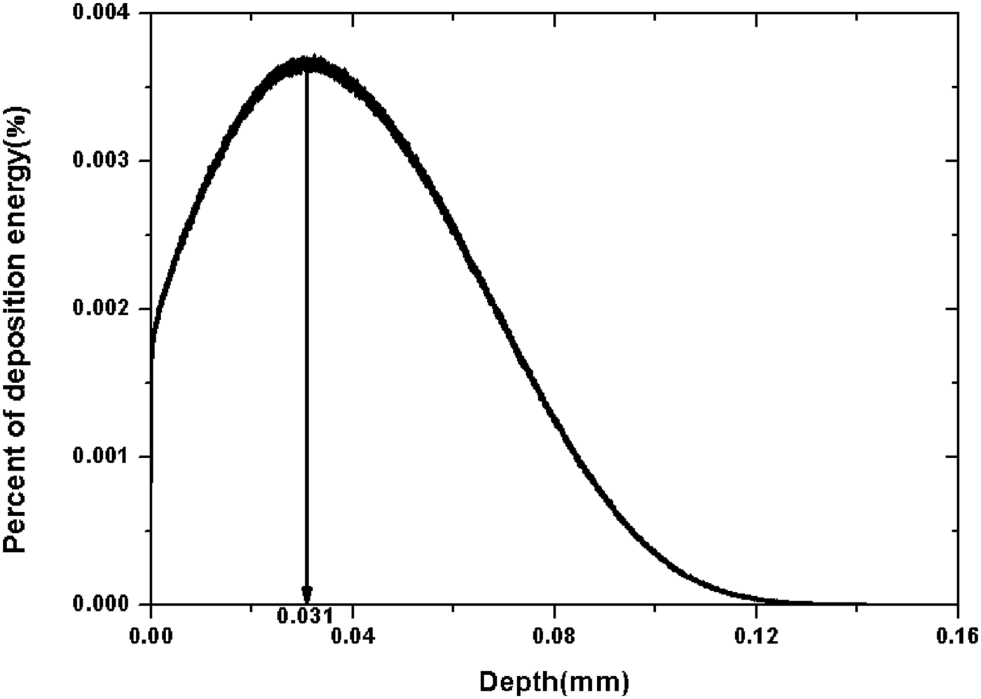
In this paper, the distribution function f(z) is calculated by the simulation code CASINO 4.24. The distribution is shown in Figure 9 with the electron energy 301 keV. The energy deposition of electron beams concentrations in the region nearby the surface of SS anode. The maximum of energy deposition is located z = 31 µm.
Fig. 9. Deposit energy versus the deposition depth with the electron energy 301 keV and SS anode.
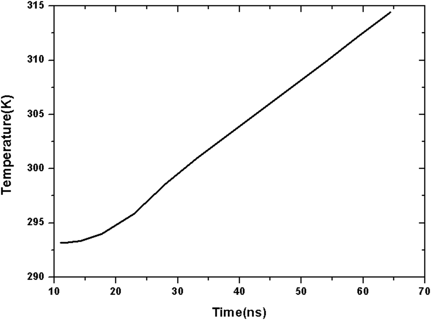
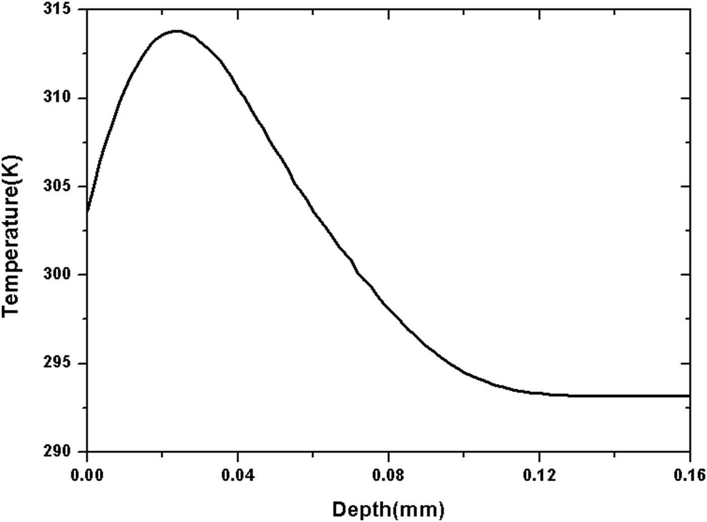
The deposited energy per unit volume W(z, t) is written as data form and imported into a finite-element software (Comsol Multiphysics 4.2a). The heat response is solved by the heat transfer module. The results are shown in Figures 10 and 11.
Fig. 10. The maximum T max versus time.
Fig. 11. The distribution of temperature along the z axial at the onset of the anode plasma.
When T 0 < t < T 1, the maximum temperature of SS anode increases with the pulse energy density and the rising rate is changing with time. When T 0 ≤ t < T 2, the rising rate keeps constant and the maximum temperature T max increases linearly. At T 2 = 63 ns, T max = 315 K. Figure 10 presents the distribution of temperature along the z axial at T 2 = 63 ns. The distribution is similar as the distribution of energy deposition of electron beams. The maximum temperature T max is located z = 23.3 µm which means the effect of heat conduction should be considered. According to the simulation results, the temperature rising of anode is less than 22 K. It indicates that the electron stimulated desorption of the contaminants dominates in the generation of the anode plasma.
3.3. The influence of the power of electron beam and A–K gap on the characteristics of the diode operated in a bipolar flow mode
The diode voltage could be increased by altering the pressure of the gas switch. The power of electron beam deposited on the SS plate with different diode voltage is presented in Figure 12. The A–K gap keeps 40 mm. Three curves present a same tendency that the amplitude of power shoots up caused by the effect of bipolar flow after the generation of anode plasma. The time for generating anode plasma T p decreases with the power deposited on the SS anode increasing. T p decreases from 55 to 37 ns with the power of electron beam increasing from ~210 to 460 MW. Altering the material of anode plate (such as brass and aluminum), the same result has been obtained. Based on the previous analysis, the generation mechanism of the anode plasma has been proved as the electron stimulated desorption of the contaminants. The scaling of desorption from a contaminator anode is in direct proportion to the product of the current density and the cross-section for stimulated desorption. The cross-section is not sensitive to the diode voltage (Cuneo, Reference Cuneo1999). Regarding the same A–K gap of 40 mm, the current density increases with the diode voltage. That is why T p decreases with the power deposited on the SS anode increasing.
Fig. 12. The power of electron beam deposited on the SS plate with different diode voltage.
The power of electron beam deposited on the SS plate with different A–K gap is presented in Figure 13. Similarly the time for generating the anode plasma T p decreases with increase of the deposit power on the SS anode under the same A–K gap (30 or 40 mm). Nevertheless, it is weird for the relationship between the T P and the A–K gap with an approximately same power of electron beam. The generation time of the anode plasma T p increases with the A–K gap decreasing. All of this would be relative with the space-charge effect caused by the electron current from cathode. Under the same power of electron beam, the space-charge effect would be more remarkable with the A–K decreasing. That is to say that the amount of ions used to neutralize the electron beam should be more than a larger A–K gap. According to our calculation reported in the other paper, the amount of ions should increase two times with the A–K gap decreasing from 40 to 30 mm.
Fig. 13. The power of electron beam deposited on the SS plate with different A–K gap.
3.4. The influence of nonuniform electron emission on the diode closure with the effect of the anode plasma
From our previous study, the temporal dependence of the plasma expansion velocity exhibits an “U”-shape with the effect of the generation of anode plasma. At the end of the plasma expansion process, the closure velocity of diode becomes higher than that at the start for the formation of anode plasma attributed to the bombardment of electron beam on the anode (Ju et al., Reference Ju, Liu and Cai2014). Generally, the effect of the fast gap closure is particularly detrimental to the long pulse diode (μs) or short A–K gap diode. In Figure 14, we present the side view images of the light from both polymer velvet cathode and brass anode. All of these were registered with a constant frame duration of 25 ns. Frame position within the pulse is indicated by the black rectangles on the waveform of the diode voltage and current (Fig. 14b). The A–K gap is 15 mm.
Fig. 14. Typical side images of the light emission from the diode. Numbered black rectangles on the current waveform indicate positions of frames with corresponding numbers.
During the time interval 35~60 ns, clear plasma was not observed at the position nearby the surface of velvet cathode and brass anode. The more intensive plasma was obtained during the time interval 75~100 ns. The light emission was not uniform over the whole cathode surface. As the high voltage pulse proceeded, brighter and larger emission centers along the periphery and the central of the cathode appeared. Corresponding to the appearance of local cathode plasma flares (or called jets), the intense anode plasma appears in the central of anode plate. It is shown that the amplitude of voltage decrease to 250 kV with a constant diode current (see in Fig. 14c). In other words, the impedance decreases during this interval. After the main part of the voltage pulse (115~140 ns), the impedance decreases further with the closure of the diode A–K gap. During the time interval 155~180 ns, the central of the diode is almost closed by the expansion of cathode and anode plasma (see in Fig. 14b). In Figure 14c, the maximum of the emission current is 4 kA in the second pulse at the low applied external voltage. The impedance of the diode collapses during the second pulse. In summary, with the effect of anode plasma, the appearance of local cathode plasma flares (or nonuniform electron emission) is particularly detrimental for the diode closure.
3.5. The effect of anode splashing on the cathode
Generally, the anode metal is destroyed under intense short-term electron bombardment in several stages, namely, plastic deformation, formation of microcraters, melting, vaporization, and splashing (Mesyats, Reference Mesyats2000). The deposited energy could be sufficient to melt the surface layer. Once the temperature and pressure in the melted region increase up to their critical values, the materials are ejected from the surface layer, forming microcraters like volcano. This splashing process is completed instantaneously. Therefore, the effects of the anode on the operation of the explosive emission cathode should also be considered. The anode materials may be deposited on the cathode surface thereby compromising the emission properties of the explosive emission cathode (Li et al., Reference Li, Liu, Zhang, Wen, Wan and Chu2014).
In our experiments, damage degree of anode plate is relative with the anode material, deposit power of electron beams, pulse number, etc. Comparing with the aluminum and SS anode, the brass anode is damaged extremely seriously. Figure 15 presents the typical plasma images of the anode surface and the picture of brass anode and polymer velvet cathode after 20 pulses. The anode plasma is not a circular spot which is not uniform over the whole anode surface (see in Fig. 15a). In Figure 15b, the brass anode is damaged extremely seriously after 20 pulses. The erosion area on the plate could be divided into two parts with different damage degree. The middle circular part is damaged seriously, and its area equal with the velvet cathode. The damage degree is not identical over this area which could be caused by the nonuniform electron emission (see in Fig. 14a). The annular part could be impacted by the electron beams from the edge of cathode and radial expansion. The damage distribution of the velvet is indeed corresponding with the middle circular part of brass plate (see in Fig. 15c). Visual inspection of the cathode revealed that patches of polymer fibers had burned, resulting in bad (discolored and browned) spots on the cathode. In addition, some fibers, random distribution, drop from the velvet cloth. There could be three reasons for the velvet cathode erosion and dropping: Drawing by electrodynamic force, burning by Joule heating effect of fiber resistance, and anode splashing.
Fig. 15. (a) The bias-side view of anode plasma, (b) the brass anode after 20 pulses, and (c) the velvet cathode after 20 pulses.
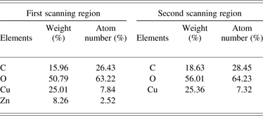
Figure 16 shows the SEM image and the energy spectrum of the polymer velvet after explosive emission using the brass anode (see in Fig. 15). Comparing with the morphological characterization of fresh velvet fiber (shown in Fig. 2b), the original smooth fibers surface are covered with big sphere particulate matter (PM) and tine dust (see in Fig. 16a). Some fibers are gooey by each other by flake material (see in Fig. 16c). In addition, fibers swell after erosion. In order to confirm the component of covering material, XEDS is used with the scanning region marked in Figures 16a and 16c. The quantitative results of compositions are listed in Table 1. As shown in Table 1, the first scanning region is composed of C, O, Cu, and Zn and the second is composed of C, O, and Cu. The concentration (wt.%) of Cu and Zn is 25.01 and 8.26%, respectively in the first region, while that of Cu in the second area is 25.36%. The appearance of Cu and Zn could preliminary confirm the effects of brass anode splashing.
Fig. 16. SEM image of polymer velvet after the interaction with pulsed electron beam (a, b), and XEDS of damage polymer velvet (c, d).
Table 1. The composition analysis of velvet surface with irradiation of pulsed electron beam
Figure 17 presents the SEM image of brass anode before and after electron-beam irradiation. The quantitative results of compositions by using XEDS are listed in Table 2. The original even surface of anode become irregularity after impacting by high-power electron beams. Craters and sphere PM bestrew the whole surface (see in Fig. 17b). As shown in Table 2, the fresh region of brass anode is composed of C, O, Cu, and Zn, which is corresponding with the compositions of the first scanning region (see in Table 1). After electron-beam irradiation, the concentration (wt.%) of C almost reduce to 0, which is similarly with the metal smelting.
Fig. 17. SEM image of brass anode before (a) and after the interaction with pulsed electron beam (b).
Table 2. The composition analysis of brass anode before and after irradiation of pulsed electron beam.
Micro-structure and elemental surface compositions of cathode are changed by the anode splashing, which is very harmful to the performance of cathode. The results of previous experiments show erosion of cathode material, which indeed affects its stability (Yang, Reference Yang2013) and lifetime (Shiffler et al., Reference Shiffler, Zhou, Bower, Lacour and Golby2004).
4. CONCLUSION
This article reports the results for a short-pulse high-power diode operated with anode effects. The bipolar flow (or anode plasma) is indeed evident at beam power densities of ~11 MW/cm2 with the pulse durations of ~50 ns. The analysis results of the deposit dose and thermal regime of the anode show the electron stimulated desorption that played an important role in the generation of anode plasma in this case. The influences of the power of electron beam and the A–K gap on the characteristics of the diode operated in the bipolar flow mode have been discussed in this paper. The time for generating the anode plasma T p decreases with increase of power deposited on the SS anode. T p increases with the A–K gap, and decrease under the same deposit power of electron beams. The fast gap closure is particularly critical for the long pulse diode (μs) or short A–K gap diode. The appearance of local cathode plasma flares (or nonuniform electron emission) is particularly detrimental for the diode closure. Once the temperature and pressure in the melted region increase up to their critical values, the materials are ejected from the surface layer. After multi-pulses, the original smooth fibers surface is coved with big sphere PM and tine dust. Some fibers are gooey by each other by flake material. The compositions of covering materials has been confirmed by XEDS, which contain the elements Cu and Zn. Micro-structure and elemental surface compositions of cathode are changed by the anode splashing, which is indeed very harmful to the performance of cathode.
ACKNOWLEDGEMENTS
The authors would like to express their gratitude to the anonymous reviewer of this paper for his valuable comments. They gratefully acknowledge support from Dr. Jianghua Zhang for his help in using the software CASINO V2.4. They would also like to thank Dr. Yanpan Hou, Dr. Cunbo Zhang and Dr. Tianyang Zhang for their help in experiments.
This work was supported by the National Science Foundation of China under Grant No. 11305263 and 61401484.