I. INTRODUCTION
With the huge development of printed circuit board technology, design procedure and modelling methods of microwave filters including low-pass filters (LPFs) have been changed. Due to low cost, repeatability, compact size and high accuracy, printed circuit filters have been widely used instead of rectangular and coaxial waveguide filters [Reference Kinayman and Aksun1].
LPFs are greatly demanded in microwave circuits to suppress undesirable harmonics and spurious signals and higher frequency rejection [Reference Chen2]. Characteristics expected from a low pass filter are very sharp transition band, broad rejection in stopband and low insertion loss in passband [Reference Pozar3]. To achieve these objectives, different design approaches such as Photonic Bandgap Structures (PBGs) [Reference Yang, Ma, Qian and Itoh4] and Defected Ground Structures (DGSs) [Reference Ahn, Park, Kim, Kim, Qian and Itoh5–Reference Kumar and Kartikeyan10] are used in the design of the LPFs.
Defected Ground Structure concept expresses that the ground plane of planar circuit is incised with periodic or non-periodic defect [Reference Kim, Park, Ahn and Jae-Bong11]. DGSs play an important role in the design problems encountered in Radio Frequency (RF)-microwave applications: power dividers, microstrip patch antennas, microwave filters, power amplifiers, Substrate Integrated Waveguides (SIWs) [Reference Hong12].
Moreover, DGSs are used to improve filter properties such as low insertion loss, deeper and wider stopband, less ripple in the passband and sharp rejection characteristics. DGSs are an alternative choice to use in printed circuit components for reduction of harmonic signals in power amplifiers. DGSs provide a solution for practically realization of a high impedance line. It is possible to reduce the size of microwave circuits and compact them via DGSs [Reference Guha and Antar13].
In order to obtain broad stopband and very sharp roll-off rate for LPFs many methods have been proposed to literature in [Reference Boutejdar, Elsherbini and Omar14–Reference Ertay, Abbak and Şimşek19]. To achieve sharp transition bands, open complementary split ring resonators (OCSRRs) are used in [Reference Aznar, Velez, Bonache, Menes and Martin15]. OCSRR filters in [Reference Aznar, Velez, Bonache, Menes and Martin15] have narrow stopband characteristics than the filters given in [Reference Tu and Chang16, Reference Park, Kim and Nam17]. A compact low pass filter with spiral microstrip resonant cells and single fan-shaped dumbbell DGS unit cell are designed in [Reference Gu and Sun18, Reference Ertay, Abbak and Şimşek19], respectively. However, papers in [Reference Park, Kim and Nam17–Reference Ertay, Abbak and Şimşek19] are not included a good sharp roll off performance for the proposed filters.
The motivation of this paper is to design a novel low pass filter with broad stopband and very sharp transition band using finite periodic Double Radial Stubs (DRSs) and fan-shaped defected ground structures (FSDGSs). For this purpose, a novel low pass filter (LPF) design procedure is proposed for electromagnetic bandgap based microstrip filters without using classical filter design approach. Proposed filter includes finite periodic DRSs and FSDGSs in the design to obtain very sharp transition band and broad stopband rejection. All of the full wave electromagnetic simulation design steps are performed in commercial software ANSYS High Frequency Structure Simulator (HFSS) based on Finite Element Method (FEM) [20] and 3D EM Simulator SONNET based on Method of Moment (MoM) [21]. The proposed LPF is fabricated and measured with Agilent 5245A PNA-X Vector Network Analyzer. The designed filter has a broad stopband characteristic better than −20 dB from 1.65 to 7.41 GHz. Roll off rate of the filter is 134.55 (dB/GHz) in the transition region. Moreover, circuit size of the designed filter is 40 mm × 20 mm. Equivalent Circuit (EC) model of designed filter is proposed and verified by using commercial software Applied Wave Research (AWR) Microwave Office [22].
II. DESIGN PROCEDURE OF THE PROPOSED LPF
In this paper we propose direct dimensional synthesis for electromagnetic bandgap based microstrip filter without using classical filter design. Electromagnetic bandgap characteristics are provided by finite periodic Double Radial Stubs on the microstrip line. DRS dimensions on the microstrip line are determined achieving a cut-off frequency (f c′) which is greater than desired cut-off frequency of filter (f c). Filter response obtained by finite periodic DRSs can be improved by DGSs on the ground plane. When the DGSs are placed to the ground plane cut-off frequency f c′ shifts to a lower frequency value. Moreover, DGSs lead to broad stopband and sharper transition from transmission band to the stopband. Due to the effects of DGSs on the ground plane, f c′ should be chosen greater than the f c. DGS dimensions should be optimized until design objectives are met. In order to design desired LPF, we propose the following design procedure:
(i) A DRS on the top layer of microstrip is modelled with equivalent circuit. Finite periodic DRSs are also modelled together with equivalent circuit and electromagnetic simulators. DRS dimensions are determined achieving a cut-off frequency (f c′) which is greater than desired cut-off frequency of filter (f c).
(ii) A FSDGS is placed on the ground layer of microstrip and it is modelled with equivalent circuit. Finite periodic FSDGSs are also modelled together with equivalent circuit and electromagnetic simulators. FSDGS dimensions are determined achieving a cut-off frequency which approaches to f c.
(iii) Parametric analyses are realized to meet design specifications. Filter dimensional parameters are tuned. Filter response is compared to circuit model and validated with measured results.
III. A DESIGN EXAMPLE
Filter characteristics are assumed to have 1.5 GHz cut-off frequency (f c), −20 dB minimum stopband attenuation and 1 dB maximum ripple in the passband.
A) Determination of DRS dimensions
In this design, there are many microstrip line sections between DRSs and it is important to analyze the effect of these line sections on the frequency characteristic of proposed LPF. To see this, short microstrip lines (l < λ g/8) can be modelled as L-shaped network as shown in Fig. 1. Microstrip lines whose physical lengths are smaller than a quarter of guided wavelength λ g can be modelled as lumped elements like L-shaped network. If l < λ g/8 then it can be obtained as
 $${\omega _c}\,{L_{\mu strip}} = {Z_0}\sin \left( {\displaystyle{{2\,\pi \,{f_c}} \over {{\upsilon _p}}}l} \right) \approx {Z_0}\left( {\displaystyle{{2\,\pi \,{f_c}} \over {{\upsilon _p}}}l} \right) $$
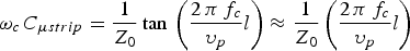 $${\omega _c}\,{C_{\mu strip}} = \displaystyle{1 \over {{Z_0}}}\tan \,\left( {\displaystyle{{2\,\pi \,{f_c}} \over {{\upsilon _p}}}l} \right) \approx \displaystyle{1 \over {{Z_0}}}\left( {\displaystyle{{2\,\pi \,{f_c}} \over {{\upsilon _p}}}l} \right) $$
where L μstrip, Cμstrip, υ p, l and Z 0 are the inductance of left/right side of short microstrip line section, the capacitance of left/right side of short microstrip line section, the corresponding phase velocity, the length of the microstrip line section, and the characteristic impedance of short microstrip line, respectively. The equivalent inductance and the capacitance of short microstrip lines are determined as L μstrip = Z 0l/υp and C μstrip = l/(Z 0υ p) via (1) and (2) [Reference Park, Kim and Nam17]. Simulated S 11 and S 21 frequency characteristics of DRS with equivalent circuit (EC) and electromagnetic simulator (HFSS) are given in Fig. 1.

Fig. 1. Double radial stub with its frequency characteristic and equivalent circuit.
A microstrip unit structure of proposed filter with two radial stubs interconnected with a cross junction structure, which means double radial stubs, is seen in Fig. 1. A cross junction which connects two radial stubs is modelled as a capacitance named C S as well as a single radial stub shown in Fig. 1 corresponds to a L-C circuit called LSRS, CSRS respectively. In order to calculate equivalent circuit parameters of a single radial stub, equations (3) and (4) given below are used [Reference Satish, Srivastava, Biswas and Kettle23]:
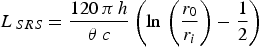 $${L_{\,SRS}} = \displaystyle{{120\,\pi \,h} \over {\theta \,c}}\left( {\ln \,\left( {\displaystyle{{{r_0}} \over {{r_i}}}} \right) - \displaystyle{1 \over 2}} \right) $$
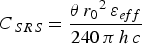 $${C_{\,SRS}} = \displaystyle{{\theta \,{r_0}^2 \,{\varepsilon _{eff}}} \over {240\,\pi \,h\,c}} $$
where ε eff, θ, h, r 0, r i, LSRS, CSRS are the effective dielectric constant, the angle of single radial stub (SRS), the substrate thickness, the side length of SRS connected to capacitive line, the side length of SRS in the capacitive line, inductance and capacitance of SRS respectively as shown in Fig. 1.
Another design step is to obtain broad stopband. For this purpose, DRSs connected with a cross junction structure is cascaded to the 50 Ω microstrip line. In order to obtain stopband characteristic by finite periodic structures considering a compact filter, it is generally sufficient to use 10 unit cells in the periodic filters. Cascading nine parts of DRSs has performed stopband characteristic as clearly demonstrated in Fig. 2. Furthermore, two different EM simulation programs, which are HFSS and SONNET, show excellent agreement. When the first step of the proposed filter design procedure is applied f c′ is chosen as 4 GHz (see Fig. 2) and DRS dimensions are obtained.
Fig. 2. Cascaded double radial stub with its frequency characteristic and equivalent circuit.
B) Determination of FSDGS dimensions
A FSDGS unit is given in Fig. 3. As mentioned in [Reference Ahn, Park, Kim, Kim, Qian and Itoh5, Reference Guo and Wang6], DGS shows various effects in printed circuits such as inductive, capacitive and resistive. Typically, it is possible to say that a fan shaped DGS unit can be modelled as a parallel RLC circuit. To extract the equivalent circuit parameters of a fan shaped DGS unit from its S-parameters, equations (5)–(9) are used [Reference Guo and Wang6]:
 $${L_{\,DGS}} = \displaystyle{1 \over {4{{(\pi {f_0})}^2}\,{C_{DGS}}}} $$
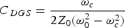 $${C_{\,DGS}} = \displaystyle{{{\omega _c}} \over {2{Z_0}(\omega _0^2 - \omega _c^2 )}} $$
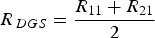 $${R_{\,DGS}} = \displaystyle{{{R_{11}} + {R_{21}}} \over 2} $$
 $${R_{\,11}} = \displaystyle{{2{Z_0} \left\vert{S_{11}}({\omega _0})\right\vert} \over {1 - \left\vert{S_{11}}({\omega _0})\right\vert}} $$
 $${R_{\,21}} = 2{Z_0}\displaystyle{{1 - \left\vert{S_{21}}({\omega _0})\right\vert} \over {\left\vert{S_{21}}({\omega _0})\right\vert}} $$
where L DGS, CDGS are inductance, capacitance of the FSDGS and R 11, R 21, R DGS are loss resistance derived from S 11(ω 0) variable, loss resistance derived from S 21(ω 0) variable, loss resistance of FSDGS respectively. Other parameters, i.e., Z 0, f 0, ω c, ω 0 are characteristic impedance of the line which is chosen 50 Ω, resonance frequency, angular cut-off frequency and angular resonance frequency of DGS unit respectively. Calculated parameters of a single FSDGS unit are L DGS = 2.790nH, C DGS = 1.117pF, R DGS = 1661.3 Ω respectively. Frequency characteristic of this structure and its equivalent circuit can be seen in Fig. 3.
Fig. 3. Fan shaped DGS with its frequency characteristic and equivalent circuit.
As a step of design procedure, we, the designers, propose to obtain very sharp transition band by cascading FSDGS resonators in the ground plane. There are, however, mutual couplings between FSDGS resonators, so these effects are needed to take into account when both performing EM simulation and extracting of circuit model of this cascaded structure. Coupling coefficient K shown in Fig. 4(a) can be calculated [Reference Wu, Chung-Hao, Tzong-Lin and Itoh24] by using equation (10)
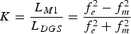 $$K = \displaystyle{{{L_{M1}}} \over {{L_{DGS}}}} = \displaystyle{{f_e^2 - f_m^2} \over {f_e^2 + f_m^2}} $$
where L m1, fe, fm are mutual inductance, two split resonance frequencies due to the mutual coupling [Reference Wu, Chung-Hao, Tzong-Lin and Itoh24].
Fig. 4. (a) Cascaded FSDGSs geometry consisting of three units and its equivalent circuit with mutual coupling. (b) Frequency characteristic of three cascaded FSDGSs.
Coupling coefficient K as shown in Fig. 2 is optimized using AWR circuit simulation tool. Purpose of the optimization is to match the circuit response of S 21 with that using EM simulation used for our study. Equivalent circuit model and frequency characteristic of cascaded FSDGSs consisting of three parts included with mutual couplings between slotted structures are demonstrated in Figs 4(a) and 4(b) respectively. EC model of this structure is in acceptable agreement with its EM simulation.
After obtaining the equivalent circuit of the cascaded FSDGSs, four different configurations including one, three, five and ten cascaded FSDGSs are simulated in HFSS and obtained results are shown in Fig. 5. Figure 5 depicts that ten cascaded FSDGSs have very sharp transition band with respect to other configurations.
Fig. 5. |S 21| frequency response of four different configurations of FSDGS for optimal design.
From the frequency response given in Fig. 5, configurations only including cascaded FSDGSs on the ground plane are not sufficient to obtain filter objectives. In order to improve roll of rate and broadening of stopband characteristic, we have to combine FSDGSs and DRSs as shown in Fig. 6.
Fig. 6. Combining of cascaded FSDGSs and DRSs.
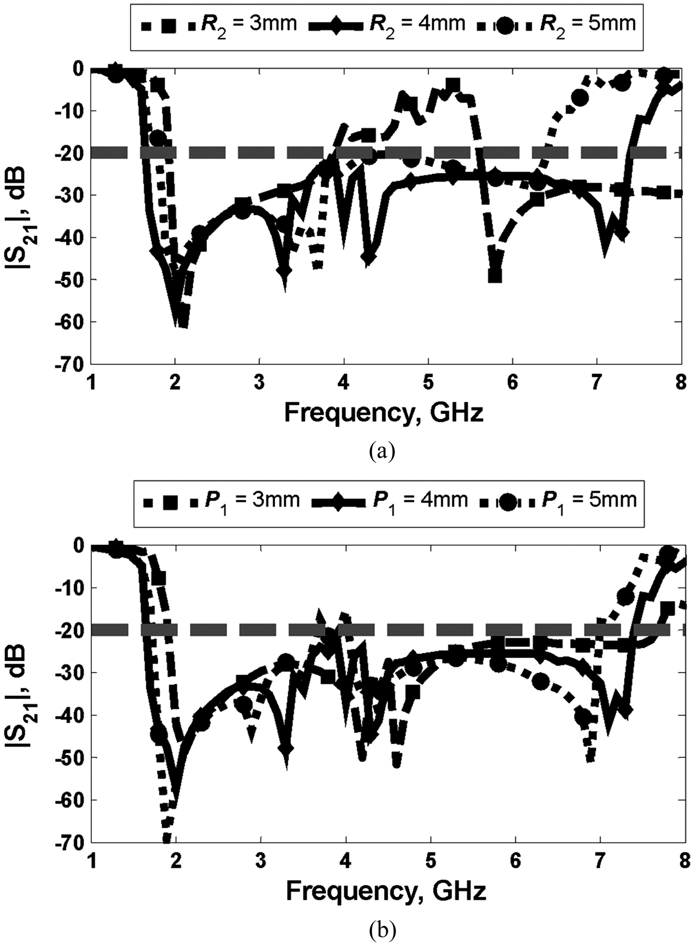
Realizing of cascaded FSDGSs with suitable R 2 values shown in Fig. 6 for each DRS provides a broad stopband as well as low-pass frequency characteristic as shown in Fig. 7(a). Additionally, it is crucial that optimal P 1 value supports a broad stopband as shown in Fig. 7(b). FSDGS dimensions are determined achieving a cut-off frequency which approaches to f c. Finally, the equivalent circuit model of the designed LPF is modelled in AWR with the equations and related S-parameters mentioned above are demonstrated in Fig. 8.
Fig. 7. (a) |S 21| frequency response of R 2 configurations of FSDGS for optimal design. (b) |S 21| frequency response of P 1 configurations of DRS for optimal design.
Fig. 8. Equivalent circuit model of designed LPF with FSDGSs and SRSs.
C) Simulated and measured results
Filter dimensional parameters are tuned after comprehensive parametric analyses. The schematic layout of the designed LPF using SRSs and FSDGSs with its final physical dimensions are shown in Fig. 9. Figure 10 demonstrates simulated EM and EC models and measurement results of the proposed LPF. As it is seen from Fig. 10, −3 dB cut-off frequency range of the filter is from 1.49 to 8.04 GHz. Note that the −20 dB stopband width is 1.65 GHz to 7.41 GHz as well as passband ripple level below 1.4 GHz is less than 0.85 dB. Maximum attenuation level and frequency in the stopband of the designed LPF is −57.2 dB and 2 GHz respectively. The maximum value of |S 11| in the passband is below −13.5 dB. Meanwhile, EM and EC simulation results are in good agreement with each other.
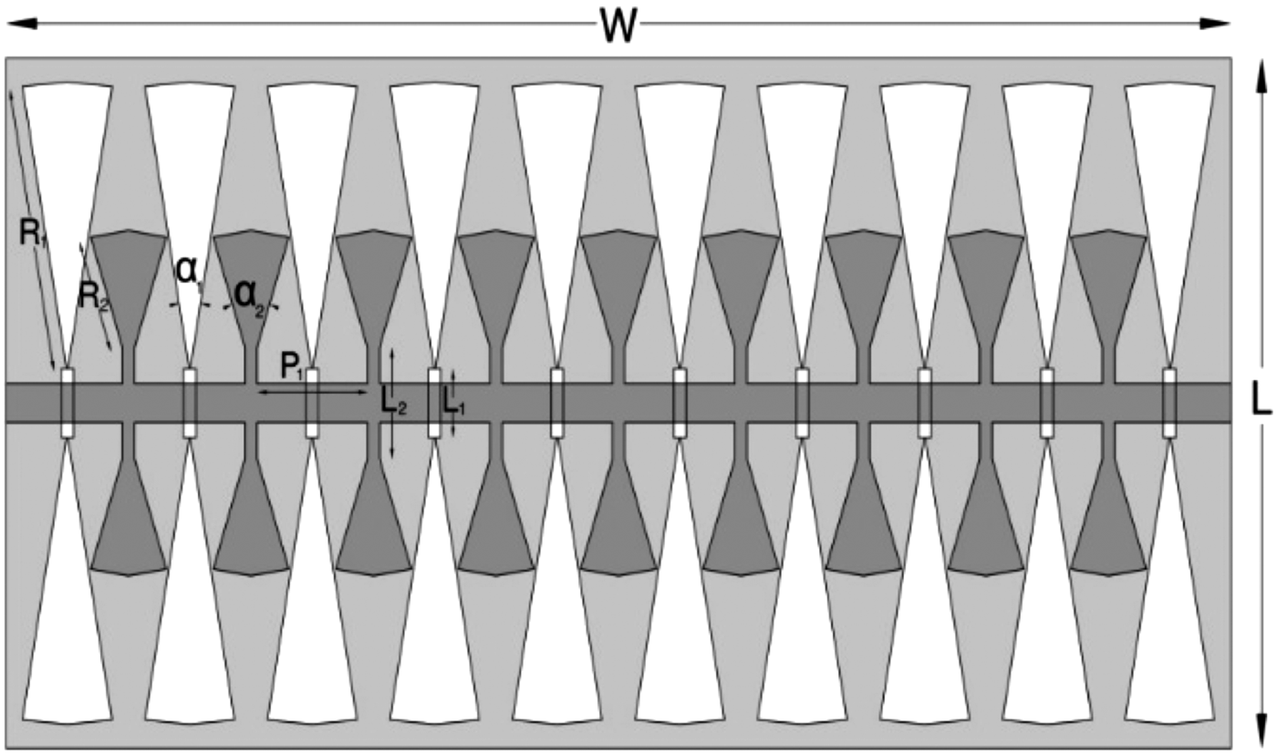
Fig. 9. Schematic layout of proposed LPF where R 1 = 8.30 mm, R 2 = 3.35 mm, α 1 = 20°, α 2 = 36°, P 1 = 3.6 mm, L 1 = 3.23 mm, L 2 = 3.23 mm, W = 40 mm, L = 20 mm.
Fig. 10. Simulated frequency responses of both EM and EC simulation of the proposed LPF.
The proposed LPF is manufactured (see Fig. 11(a)) on an ARLON AD 1000 substrate which is specified by a dielectric constant of 10.2, dielectric loss tangent of 0.0023 and a thickness of 1.27 mm. The input and output feed lines have 1.12 mm line width of corresponding to a 50 Ω microstrip line. The fabricated LPF as shown in Fig. 11(a), is measured in the range of 0.8–8 GHz via Agilent 5245A PNA-X vector network analyzer. Figure 11(b) shows that EM simulation and measurement results of the proposed LPF are in close agreement. Additionally, a conventional stepped impedance microstrip lowpass filter by using classical filter approximation [Reference Hong12] is designed in AWR and compared with the proposed LPF.
Fig. 11. (a) Top and bottom photograph of fabricated filter respectively. (b) Measured and simulated frequency responses of designed LPF.
As clearly shown in Fig. 11(b), the conventional stepped impedance LPF has 0.5 dB passband ripple level, 179.28 mm × 7.62 mm physical dimension. Although stopband characteristic of the conventional stepped impedance LPF is better than the proposed one, it has very big size whereas the proposed LPF has 40 mm × 20 mm. Due to this case, the conventional stepped impedance LPF is difficult to integrate in applications where small size are required.
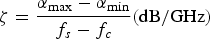
To compare the designed LPF with recently published works, some arguments which is important for filter design are described by (11) and (12):
 $$\zeta = \displaystyle{{{\alpha _{{\rm max}}} - {\alpha _{{\rm min}}}} \over {{f_s} - {f_c}}}({\rm dB/GHz}) $$
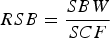 $$RSB = \displaystyle{{SBW} \over {SCF}} $$
where ζ, α max, α min, f s, fc, RSB, SBW, SCF are roll of rate, the −40 dB attenuation point, the −3 dB attenuation point, the −40 dB stopband frequency, the −3 dB cut-off frequency, relative stopband bandwidth, stopband bandwidth, stopband center frequency, respectively.
Table 1 indicates the performance comparison of the designed LPF with the previous reported works in the open literature. The results shown in [Reference Aznar, Velez, Bonache, Menes and Martin15] contain better roll off rate but it has lower RSB and higher |S 11max| values in the passband compared with the proposed LPF. The results in [Reference Tu and Chang16–Reference Gu and Sun18] show better |S 11max| values but they have lower roll off rate and RSB values according to the proposed LPF. [Reference Taher25] has better roll off rate and RSB value but it is not compact with respect to the proposed LPF. [Reference Kufa and Raida26] shows the worst filter performance in terms of these properties summarized in Table 1. The designed filter has not a good passband ripple level but it shows lower cut-off frequency response than [Reference Tu and Chang16–Reference Gu and Sun18, Reference Taher25, Reference Kufa and Raida26] except [Reference Aznar, Velez, Bonache, Menes and Martin15] as well as compact size in accordance with [Reference Park, Kim and Nam17, Reference Taher25, Reference Kufa and Raida26].
Table 1. Comparisons of proposed filter with reported works. Measured performances in different operating conditions.
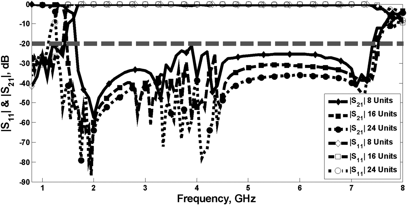
Maximum attenuation level is −57.2 dB at 2 GHz as shown in Fig. 11 for nine unit cells in the design. When the number of unit cell is increased more suppression levels than given in Fig. 11 can be obtained. In this context calculated amplitude responses of filters comprised of 8, 16 and 24 cascaded unit cells are given in Fig. 12 to demonstrate effect of number of unit cell. From the Fig. 12, we see that stopband level can be improved by increasing the number of unit cells used in the filters. It should be noted that when the unit cell numbers are increased higher stopband suppression level can be achieved. However, this improvement will extend filter length.
Fig. 12. Effect of number of unit cell on the frequency characteristic of the designed filter.
IV. CONCLUSION
In this paper a novel low pass filter (LPF) design procedure is proposed for electromagnetic bandgap based microstrip filters without using classical filter design approach. Finite periodic FSDGSs and DRSs are used in this design to achieve very sharp transition band and broad stopband. The proposed LPF is rather compact as 40 mm × 20 mm, has passband from dc to 1.49 GHz, broad stopband better than −20 dB from 1.65 to 7.41 GHz and 134.55 (dB/GHz) sharp roll off rate. Simulation results are verified by ANSYS's High Frequency Structure Simulator (HFSS) and 3D EM Simulator SONNET and validated with measurement of fabricated filter. Measured and simulated results are in good agreement and demonstrate the applicability of the proposed filter.
Agâh Oktay Ertay received his B.S. degree in electronics and communication engineering (ECE) from Yildiz Technical University in 2010 and received his M. S. degree in telecommunication engineering from Istanbul Technical University (ITU) in 2014. He has been working as a research assistant at the ECE department of ITU since 2011. His main research interests are electromagnetic theory, microwave engineering, design and implementation of microwave filters.
Mehmet Abbak received the B.S. degree from Telecommunications Engineering Department of Sabanci University in 2006, and the M.S. degree from Electronics Engineering Department of Sabanci University in 2008. He is currently continuing his Ph.D. degree in Istanbul Technical University. He has been working as a researcher in MITOS Microwave Company since 2010. His research interests are passive components in microwave including printed microstrip antennas, filters, and UWB antennas towards microwave imaging.
Serkan Şimşek received the B.S. degree in electrical and electronics engineering from Istanbul University, Istanbul, Turkey, in 2001, the M.S. and Ph.D. degrees in electronics and communication engineering (ECE) from Istanbul Technical University (ITU), Istanbul, Turkey, in 2003 and 2008 respectively. He is currently an Associate Professor at the ECE Department of ITU. His research includes guided wave theory, periodic structures and photonic crystals.