


Introduction
Ultra-wideband (UWB) radio technology has been getting increasingly popular for high-data high-speed wireless connectivity. The Federal Communications Commission (FCC) is a decision to permit the unlicensed operation band from 3.1 to 10.6 GHz [1]. In the UWB systems, UWB band-pass filters (BPFs), as one of the essential components, are designed via different methods and structures in recent years. Various new topologies to design UWB BPF are reported [Reference Sun and Zhu2, Reference Hao and Hong3]. A UWB BPF with a band notch was propounded in [Reference Ghatak, Sarkar, Mishra and Poddar4], so that in this paper, it shows that the notch-band frequency could be tuned by changing the impedance ratio of the embedded stepped-impedance resonator (SIR). Another novel compact UWB BPF with triple sharply notched bands and good selectivity was proposed using a parallel U-shaped defected microstrip structure [Reference Wang, Zhao and Li5]. Lately, a novel ring resonator BPF was reported in [Reference Nakhlestani and Hakimi6], having a wide bandwidth and high selectivity and wide stop band. An asymmetric dual-line coupling strip was provided main two paths for the signals, as propounded in [Reference Song, Pan and Xue7], makes it possible to generate multiple transmission zeroes. A new UWB BPF using triangle-ring multi-mode stub-loaded resonator (MM-SLR) was presented in [Reference Wu, Chen and Chen8], so that there are five resonant modes generated in the UWB pass band, including two odd modes and three even modes. Design of reconfigurable miniaturized UWB BPF with the tuned notched band was reported in [Reference Mohamed, El-Shaarawy, Abdallah and El-Hennawy9], consisting of compact 2U-shaped defected ground structure (DGS) resonators shunt connected to parallel coupled lines to achieved frequency notch. An UWB BPF with a notch band at 5.8 GHz and wide stop band using dumbbell stubs were propounded in [Reference Chen, Wei, Shi and Gao10], which constructed with multiple-mode resonator (MMR) using novel dumbbell stubs and one-arm-folded interdigital coupled lines in the input and output sides. The MMR consists of three pairs of shunt dumbbell stubs and a high-impedance microstrip line. A novel approach was introduced in [Reference Nosrati11] with a new configuration to design an UWB BPF double/single notch bands using micro-strip transmission lines without using any via-hole was presented, so that it was established using two parallel SIRs, providing two paths with different electrical lengths. Various structures have been presented to implement the fixed notch bands in the pass band of the UWB BPFs [Reference Hong and Lancaster12–Reference Wong and Zhu21]. Moreover, the UWB BPF filters with tunable notched band become more and more important for the future cognitive radio system. In this paper, a UWB BPF using MMR driven by coupled lines at both ends with a sharp notched band is proposed. To validate the design and analysis, a UWB BPF with a notch band is designed, simulated by the ADS simulator and fabricated on a 31 mil thick RT/Duorid 5880 substrate with a relative dielectric constant 2.2 and loss tangent of 0.0009. Rest of the paper contains the filter design procedure as presented in the Section “Filter design”. The analysis of the proposed filter is presented in the Section “Analysis of the proposed filter” which followed by results and discussion in the Section “Simulation and measurement result”. Also the software Tecplot 9.0 is used for analyzing all structures.
Filter design
The layout of the proposed filter in this paper is shown in Fig. 1. The proposed filter consists of a modified elliptical-ring MM-SLR and asymmetric coupled input/output (I/O) lines. The dimensions of the proposed filter are shown in the following figure.

Fig. 1. The layout of the proposed UWB filter, the dimensions in Fig. 1 are L 1 = 7.6 mm, L 2 = 1.95 mm, L 3 = 6.9 mm, L 4 = 3.28 mm, W 1 = 0.3 mm, W 2 = 0.3, W 3 = 0.2, W 4 = 2.2, W 5 = 0.1.
The filter design procedure is as follows: firstly, an SIR, certainly an initial UWB, has been reported in Fig. 2 and is used as a main structure of the present filter. Frequency response of the basic proposed filter, so as band stop response with four resonant modes at the beginning and end frequency response is presented in Fig. 2.

Fig. 2. The layout and the frequency response of basic proposed UWB filter.
Secondly, by adding the asymmetric interdigital coupled I/O lines in Fig. 3, it can be achieved to UWB band-pass response. In some literature, interdigital coupled lines have been widely used as a capacitive coupling element in BPFs. If this SIR is properly fed with two interdigital parallel-coupled lines with an increased coupling degree, a UWB pass band can be achieved. As seen in frequency response, there are three resonant modes in band-pass response, achieving an upper stop band up to more than 15.85 GHz with high attenuation −27 dB. The proposed filter has a wide pass band from 4.167 to 10 GHz with insertion loss is better than 1 dB and return loss is <6.773 dB.

Fig. 3. The layout and the frequency response of add coupled lines (I/O).
Thirdly, by adding two bend to the middle resonator in Fig. 4, it can be miniaturized the size of the proposed filter and created a notch band at 6.86 GHz. In frequency response, there are five resonant modes generated in the UWB pass band, also has an upper stop band up to more than 16.44 GHz with high attenuation −39.8 to −42.14 dB. The proposed filter has a wide pass band from 3.733 to 10.38 GHz with insertion loss is better than 1 dB and return loss is <10.246 dB.

Fig. 4. The layout and the frequency response of add two bend to the middle resonator.
Figure 5 shows the current densities of resonators in pass-band frequency. The current densities of resonators without angle bend in frequency 6.86 GHz are shown in Fig. 5(a) and the current densities pass through the resonator. The current densities of resonators with two angles bend in frequency 6.86 GHz are shown in Fig. 5(b), and the current densities cannot pass through the resonator so stop at the notch band.

Fig. 5. Current densities of resonator (a) without angle bend and (b) with angles bend.
Finally, in order to improve the pass-band performances, rectangular slots were proposed as shown in Fig. 6. Moreover, the use of rectangular slots in SIR has the ability to effectively improve the pass-band characteristics and stop band width because the current densities cannot pass through the middle resonator so stop at the slot. In frequency response, there are five resonant modes generated in the UWB pass band, achieving an upper stop band up to more than 16.32 GHz with high attenuation of −39.785 to −41.968 dB. The proposed filter has a wide pass band from 3.776 to 10.42 GHz with insertion loss is better than 0.65 dB and return loss is <11 dB.

Fig. 6. The layout and the frequency response of add rectangular slots in SIR resonator.
Figure 7 shows the current densities of resonators at 2f 0 (stop-band frequency). It can be noticed that in Fig. 7(a) the current densities pass through the resonator. For the resonator in Fig. 7(b), the current densities cannot pass through the resonator so stop at the slot.

Fig. 7. Current densities of the resonator (a) SIR resonator and (b) rectangular slots SIR resonator.
Analysis of the proposed filter
Notch-band control based on analytical approach
As known, the exclusive use of the spectrum without causing interference to other existing services, such as wireless local – area network, should be considered to provide enough protection from harmful interference from generic UWB applications for existing radio systems. To circumvent this issue, single [Reference Zhu, Sun and Li22–Reference Li, Kurita and Matsui28], or multiple [Reference Li, Kurita and Matsui28], narrow-band-notched UWB filters were presented. Using slot line or open-circuited stubs into the filtering topologies, a notch or narrow rejection band can be generated in a certain frequency range in the UWB pass band. By emphasizing this issue, in the proposed filter, the notch band can be controlled using change the length of the asymmetric coupling with formula (1), which is based on empirical method. By reducing the length l 3 from 7.7 to 4.3 mm, as shown in Fig. 8(a), the notch band shifts to high frequencies as depicted in Fig. 8(b).Values of l 3 and notch-band frequency are summarized in Table 1.

Fig. 8. (a) Configuration and (b) the frequency response of the changes notch band.
Table 1. Values of l 3and the notch frequency.

The equation between the notch-band frequency and length l 3 is approximated as a linear equation as shown in Fig. 9. The relation between the notch-band frequency and l 3 can be presented as:
 $$f_{{\rm notch}\;{\rm band}}({\rm GHz}) = ( - 0.436)\;l_3 + 9.775,\quad {\rm if}\;4.3. \le l_{3}({\rm mm}) \le 7.7.$$
Fig. 9. Chart notch-band frequency changes according to the lengt l 3.
In Fig. 9, (f(GHz) is the notch-band frequency, x = l 3(mm), a and b are constants as defined in equation (1).
L–C Method
The equivalent LC circuit of this resonator is exhibited in Fig. 10. As illustrated, L 1, L 2, L 3, C 1, C 2, C 3 are inductances and capacitances of the open stubs, L bend and C bend are inductances and capacitances of the angle bend, respectively. The values of those parameters can be extracted by exploiting the methods discussed [Reference Song, Hu, Fan and Xue29], and summarized in Table 2.

Fig. 10. (a) Middle resonator structure (b) equivalent circuit of the basic designed filter.
Table 2. Element values used in the equivalent circuit of the basic designed filter.

Simulation and measurement result
The EM simulations of the proposed BPF are performed by using ADS-simulator. The Simulated/measured S-parameters of the designed UWB BPF filter and photograph of the fabricated filter are shown in Fig. 11. The overall size of the fabricated UWB BPF is 19.68 × 2.2 mm2, nearly 0.61λ g × 0.068λ g, where λ g is the guided wavelength at the center frequency. The measured results of the filter have 3 dB fractional bandwidth of 115%, with insertion loss is better than 0.65 dB and return loss is <11 dB. The comparison of the UWB proposed filter with other designs is summarized in Table 3. The superior features indicate that the BPF has a potential to be utilized in the modern UWB wireless communication systems.
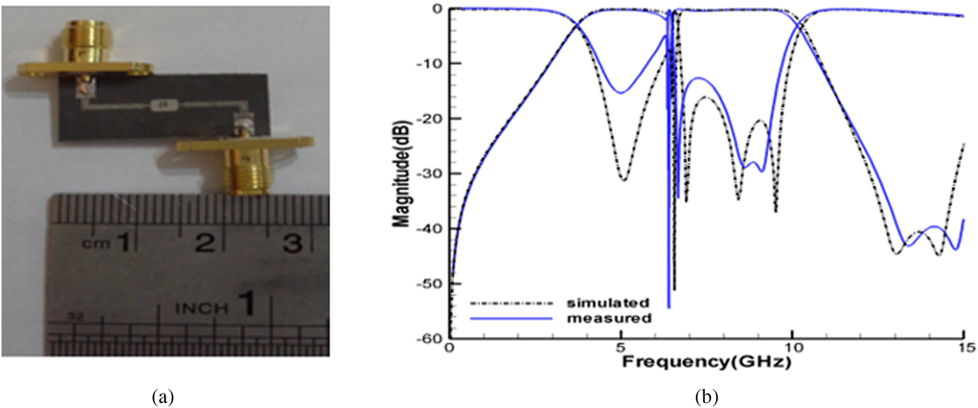
Fig. 11. Fabricated proposed filters (a) photograph (b) simulated and measured.
Table 3. Comparisons with other proposed filters. (λ g is the guided wavelength on the substrate at the center frequency.).

Patently, the error between simulation and measurement results is due to the SMA connectors loss and fabrication tolerance. Table 3 summarizes comparison between the proposed filter with another one.
Conclusion
In this paper, a compact UWB BPF (3.776–10.42 GHz) with a notched band using the SIR and coupled lines is proposed. A notch band (6.86 GHz) is created and tuned by angle bend based on the mathematical method. By adding the asymmetric tight coupled lines resonator via I/O lines, it can be achieved UWB band-pass response. In frequency response, there are five resonant modes generated in the UWB pass band, achieving an upper stop band up to more than 16.32 GHz with high attenuation −39.785 to −41.968 dB. The fabrication filter has low insertion loss, simple structure, and compact size that these performances are very useful for telecom communication. Both measured and simulated results are in good agreement.
 Gholamreza Karimi received his BS, MS, and Ph.D. degrees in Electrical Engineering from Iran University of Science and Technology, Tehran, Iran, in 1999, 2001, and 2006, respectively. Since 2007, he has been with the Electrical Department, Razi University, Kermanshah, Iran, where he is now an Associate Professor. His main research interests are low-power analog and digital IC design; RF IC design; and modeling and simulation of RF/mixed-signal IC. He is also interested in microwave devices and artificial intelligence systems.
 Fatemeh Javidan was born in Kangavar, Kermanshah, Iran in 1992. She received her B.Sc. degree in Electronics Engineering from Islamic Azad University, Tuyserkan, Hamedan, Iran in 2013 and M.Sc. degree in Electronics Engineering from Islamic Azad University, Kermanshah, Iran in 2015, respectively. Since 2014, she has been with the Electrical Department, Kangavar Azad University, Kermanshah, Iran, where she is now a Lecturer. Her current research includes microwave passive circuits, RF integrated circuit design, and photonic integrated circuit.
 Amirhossein Salehi was born in Kangavar, Kermanshah, Iran in 1983. He received his B.Sc. degree in Electronics Engineering from Islamic Azad University, Tuyserkan, Hamedan, Iran in 2010 and M.Sc. degrees in Electronics Engineering from Islamic Azad University, Kermanshah, Iran in 2015, respectively. Since 2013, he has been with the Electrical Department, Kangavar Azad University, Kermanshah, Iran, where he is now a Lecturer. His current research includes microwave passive circuits, RF integrated circuit design, and photonic integrated circuit.


