


1. INTRODUCTION
The advantages of latest developments in radio frequency (RF) and microwave engineering domain, such as low temperature co-fired ceramics (LTCC) [Reference Weng, Guo, Shi and Chen1], low-temperature co-fired ferrites (LTCF) [Reference Weng, Guo, Shi and Chen1], photonic bandgap (PBG) structures or electromagnetic bandgap (EBG) structures [Reference Hong and Karyamapudi2], ground plane apertures (GPA) [Reference Sharma3, Reference Maloratsky4], defected ground structures (DGS's), defected microstrip structures (DMS's) [Reference Mendez5, Reference Yang and Xue6], substrate integrated waveguides (SIW)[Reference Zhang7], metamaterials or complementary split-ring resonators (CSRR) [Reference Xu and Alphones8, Reference Martin, Falcone, Bonache, Marques and Sorolla9], have helped to improve performance capabilities of microwave components/circuits [Reference Arya, Kartikeyan and Patnaik10]. This, in turn, has made possible achievement of compact and smart devices and components with enhanced features. The PBG structure is a periodic structure in which the propagation of energy in certain bands of frequencies is inhibited. The EBG structures are generally known as PBG structures [Reference Arya, Kartikeyan and Patnaik10]. However, it is difficult to use a PBG structure for the design of the microwave or millimeter-wave components due to difficulties in modeling because too many parameters namely, lattice period, shape, size, and location, are to be mitigated [Reference Weng, Guo, Shi and Chen1]. Another problem in using these PBG circuits is the radiation from periodically etched defects [Reference Weng, Guo, Shi and Chen1, Reference Hong and Karyamapudi2, Reference Arya, Kartikeyan and Patnaik10]. These disadvantages of PBGs/EBGs led to the evolution of DGS's. The DGS is a simple yet a powerful variant of PBGs in which a part of the ground plane metal of microstrip circuit is intentionally modified to enhance the performance. DGS cells have inherent resonant properties and many of them have been applied in the design of filter circuits.
The recent concept of metamaterials has also attracted the attention of researchers in the field of microwave engineering for designing of specific microwave components. Metamaterials are broadly defined as artificial effectively homogeneous electromagnetic structures with unusual properties not readily available in nature [Reference Caloz and Itoh11, Reference Marqués, Martín and Sorolla12]. Metamaterial structures, also known as left-handed (LH) metamaterial structures were proposed by Victor Veselago in 1968. The medium is characterized by a simultaneous negative electric permittivity and negative permeability [Reference Caloz and Itoh11]. Metamaterial can also be described as EBG/PBG or DGS when the length of period is much smaller in physical size than the wavelength of electromagnetic wave travelling through the structure [Reference Caloz and Itoh11, Reference Elsheakh, Elsadek and Abdallah13]. For the metamaterial, the structure size should be less than a quarter wavelength whereas in DGS or EBG/PBG, this is not necessary [Reference Elsheakh, Elsadek and Abdallah13].
In addition to all these developments, serious efforts are also in progress in metamaterials to obtain engineered media with tailor made properties (single or double negative) of permittivity and permeability to achieve controllable bandpass and bandstop characteristics [Reference Martin, Falcone, Bonache, Marques and Sorolla9]. However, it is rather difficult to design and realize engineered metamaterials for generalized applications. This is overcome by DGS, which is very simple to design and fabricate. The DGS is realized by etching of a simple shape in the ground plane. Depending on the shape and dimensions of the defect, the shielded current distribution in the ground plane is modified, resulting in a controlled excitation and propagation of electromagnetic waves through the substrate layer. The shape of defect may be changed from a simple to a complicated one depending on the application with better or desired performance [Reference Arya, Kartikeyan and Patnaik10].
2. PBG/EBG, METAMATERIAL, AND DGS/GPA STRUCTURE
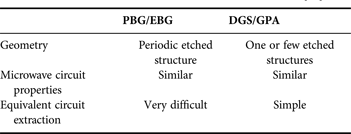
As mentioned earlier, the DGS is an etched lattice shape (slot) and is located on the ground plane of the microstrip line. It is motivated by a study of PBG to change guided wave properties. DGS is made out of one or a few of PBG etched ground elements. The shape of DGS slot is modified from a simple hole to a more complicated shape [Reference Arya, Kartikeyan and Patnaik10]. The DGS structure may be found in both one-dimensional [Reference Kim, Park, Dal and Kim14, Reference Xue, Shum and Chan15] and two dimensional forms [Reference Radisic, Qian, Coccioli and Itoh16]. Table 1 shows the basic difference between PBG/EBGs and DGSs. The geometry of DGS is simpler than the PBG/EBG. The circuit modeling is simpler for DGS compared to the other topologies.
Table 1. Differences between EBG/PBG and DGS/GPAs [Reference Arya, Kartikeyan and Patnaik10].
3. CLASSIFICATION OF DGS CONFIGURATION
A flow chart of the classification of DGS structures has been shown in Fig. 1. The shape of the slot affects the response of the DGS unit section. For this, it is divided into two categories. The first one is a rectangular slot without the head and the second category is a rectangular slot with different head shapes (e.g. circular, square, arrow, etc.). In Fig. 2, the DGS geometries have been reported so far that includes simple shapes such as rectangular dumbbell [Reference Guha, Biswas and Antar17, Reference Ahn, Park, Kim, Kim, Qian and Itoh18], circular dumbbell [Reference Park19], spiral [Reference Kim, Lim, Nam, Kang and Ahn20], U-shaped [Reference Woo, Lee, Lee, Pyo and Choi21], V-shaped [Reference Woo, Lee, Lee, Pyo and Choi21], H-shaped [Reference Mandal and Sanyal22], cross-shaped [Reference Chen23], concentric rings [Reference Guha, Biswas, Biswas, Siddiqui and Antar24], etc. Some more complex DGS structures such as split ring resonators [Reference Hou25, Reference Burokur, Latrach and Toutain26] or fractals [Reference Liu, Li and Sun27] have also been examined.
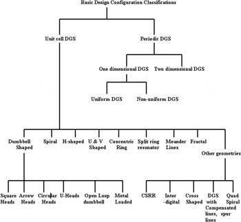
Fig. 1. Flow chart of various DGS configurations [Reference Guha, Biswas and Antar17].
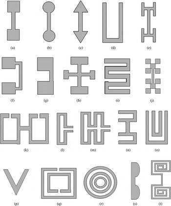
Fig. 2. Different DGS geometries: (a) dumbbell-shaped [Reference Guha, Biswas and Antar17, Reference Ahn, Park, Kim, Kim, Qian and Itoh18], (b) circular head dumbbell, (c) arrow head dumbbell [Reference Abdel-Rahman, Verma, Boutejdar and Omar42], (d) U-shaped [Reference Woo, Lee, Lee, Pyo and Choi21, Reference Woo, Lee, Pyo and Choi43], (e) H-shaped [Reference Mandal and Sanyal22], (f) square heads connected with U-slots [Reference Woo, Lee, Lee, Pyo and Choi21], (g) square slots connected with narrow slot at edge [Reference Breed44], (h) cross-shaped [Reference Mandal and Sanyal22, Reference Chen23], (i) inter-digital [Reference Balalem, Ali, Machac and Omar45], (j) Fractal [Reference Liu, Li and Sun27], (k) open loop dumbbell [Reference Guha, Biswas and Antar17], (l) L-shaped [Reference Hong and Karyamapudi46], (m) meander lines [Reference Breed44, Reference Boutejdar, Omar, Batmanov and Burte47], (n) U-head dumbbell [Reference Breed44], (o) double equilateral U [Reference Kim and Lee48], (p) V-shaped [Reference Woo, Lee, Lee, Pyo and Choi21], (q) split-ring resonators [Reference Hou25, Reference Burokur, Latrach and Toutain26], (r) concentric ring shaped [Reference Guha, Biswas, Biswas, Siddiqui and Antar24], (s) half-circle [Reference Boutejdar, Sherbini, Ali, Fouad, Ahmed and Omar49], and (t) spiral-shaped [Reference Kim, Lim, Nam, Kang and Ahn20].
Some other geometries proposed in the literature are periodic DGSs [Reference Caloz, Okabe, Iwai and Itoh28–Reference Oskouei, Forooraghi and Hakkak30], DGS with inverted microstrip [Reference Ha and Kwon31], asymmetric crossed-shaped [Reference Chen32], Hilbert curve ring [Reference Chen, Weng, Jion and Zhang33], stepped hairpin shaped [Reference Dahlan, Aizam and Shipun34], hexagonal shaped [Reference Zulkifli, Rahardjo and Hartanto35], coupled C-shaped [Reference Boutejdar, Elsherbini and Omar36], multi-ring resonator [Reference Boutejdar, Batmanov, Elsherbini, Burte and Omar37], L-shaped [Reference Hamad, Safwat and Omar38], E-shaped [Reference Huang and Lee39], and T-stub shaped [Reference Luo, Ma, Li and Ma40]. These structures are used to implement specific filters, to suppress unwanted surface waves, and to control harmonics in microstrip antennas, and in a variety of compact microwave circuits. Different geometries have been explored with the aim of achieving improved performance in stopband and passband characteristics, compactness, and comfort in fabrication [Reference Yun and Shin41].
4. MICROSTRIP LINE WITH AND WITHOUT DGS UNIT CELL
In this section, the basic difference in transmission characteristics of a microstrip line with and without a DGS is shown illustriously in Fig. 3(a), a 50 Ω microstrip line without any defect in the ground is shown. The dimensions and material properties of this microstrip line are: width W = 3.6 mm, length L = 19.5 mm, substrate height H = 1.524 mm, conductor thickness t = 0.07 mm, and the substrate is Neltec (NH 9320) with permittivity = 3.2 and loss tangent = 0.0024. This 50 Ω microstrip line is simulated in the HFSS V10 full wave electromagnetic (EM) simulator to examine the transmission properties. Figure 3(b) shows the simulated results of this 50 Ω microstrip line from which it is evident that the whole signal is passing without attenuation for the frequency range of 1–10 GHz. When the metal is etched in the shape of a dumbbell with square heads, connecting with a slot in the ground plane of microstrip (shown in Fig. 4(a)), then it is called a microstrip line with DGS and the dimensions of the DGS unit cell are “a” and “g” where “a” is the dimension of the square head and “g” is slot gap and the length of the connecting slot is L. Figure 4(b) shows the simulated transmission characteristics of the 50 Ω microstrip line with DGS using the HFSS. From these investigations, it is clear that the microstrip line exhibits bandstop response and it is due to the DGS with effective inductance and capacitance working in parallel. The frequency characteristics of the DGS section can be explained by two parameters: one is lattice dimensions and the second is gap distance. Effective inductance and capacitance can be calculated using [Reference Arya, Kartikeyan and Patnaik10]:
 $$L = \displaystyle{1 \over 4\pi ^2 f_o^2 C}\comma \;$$
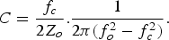 $$C=\displaystyle{f_c \over 2Z_o}. \displaystyle{1 \over 2\pi \lpar f_o^2 - f_c^2 \rpar }.$$
Fig. 3. (a) 50 Ω microstrip line without DGS. (b) Simulated S-parameter without DGS.
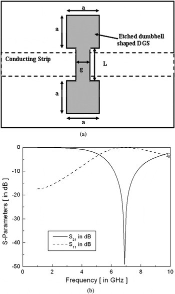
Fig. 4. (a) 50 Ω microstrip line with DGS. (b) Simulated S-parameter with DGS [Reference Yun and Shin41].
If we look retrospectively, the current flow is changed on the ground plane with the etched DGS as shown in Fig. 5(a).
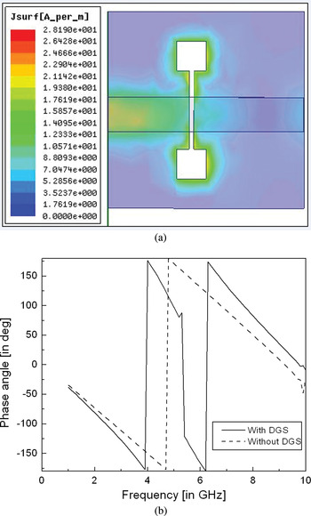
Fig. 5. (a) Magnetic current distribution in the square dumbbell-shaped DGS at the resonance frequency. (b) Simulated phase angle jumping phenomenon with and without DGS.
In addition, the phase also changes rapidly and is shown in Fig. 5(b). This slows down phase velocity of the signal. This phenomenon of slow phase velocity is called slow wave effect and it can be analyzed in terms of slow wave factor (SWF) [Reference Arya, Kartikeyan and Patnaik10].
A) Characteristics of DGS
There are two main characteristics of DGS: one is slow wave effect in the passband and the second is bandstop characteristics.
1) SLOW-WAVE EFFECT IN PASSBAND
Figure 5(b) shows the jumping phenomenon that occurs at resonant frequency (f o). As compared with the microstrip line without DGS, the microstrip line with DGS shows a fast phase variation that exhibits slow-wave behavior below the resonant frequency (f o) and a slower phase variation that shows fast wave behavior beyond the resonant frequency (f o). In another way, the same phenomenon can be described as follows [Reference Arya, Kartikeyan and Patnaik10, Reference Liu, Li, Sun, Kurachi, Chen and Yoshimasu50]:
When f < f o (frequencies less than the resonance frequency of defect),  $2\pi f_o L\lt \displaystyle{1 \over 2\pi f_o C}$, the inductive nature of microstrip line is dominant.
When f > f o (frequencies greater than the resonance frequency of defect),  $2\pi f_o L\gt \displaystyle{1 \over 2\pi f_o C}$, the capacitive nature of microstrip line is dominant.
When f = f o, (at the resonance frequency), 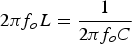 $2\pi f_o L = \displaystyle{1 \over 2\pi f_o C}$, the jumping phenomenon occurs.
2) BANDSTOP PROPERTIES
From the equivalent circuit of DGS unit section shown in Fig. 6, due to the DGS unit cell, series inductance increases the reactance of microstrip with increase of the frequency. Thus, the rejection of certain frequency bands can be started. Parallel capacitance with series inductance provides the attenuation pole location, which is the resonance frequency of parallel LC resonator. As the frequency increases, reactance of the capacitor decreases [Reference Arya, Kartikeyan and Patnaik10, Reference Liu, Li, Sun, Kurachi, Chen and Yoshimasu50]. Hence, the bandgap between the propagating frequencies occurs as shown in Fig. 4(b).

Fig. 6. RLC circuit modeling of unit DGS cell [Reference Weng, Guo, Shi and Chen1].
5. L-C CIRCUIT MODELING OF UNIT DGS CELL
It is very difficult to implement DGS in LC resonator without terminating the harmonics and also to obtain excellent stopband and passband characteristics [Reference Weng, Guo, Shi and Chen1]. Hence, accurate equivalent circuit of DGS can be modeled as a π-RLC equivalent circuit rather than a simple LC equivalent circuit. The π-RLC equivalent circuit is shown in Fig. 6, with circuit parameters which can be expressed in terms of ABCD or S-parameters [Reference Weng, Guo, Shi and Chen1, Reference Haiwen, Xiaowei and Zhengfan51].
Here, R is resistance; L is inductance; C is capacitance; G p is conductance offered by microstrip line; C p is capacitance of microstrip line; Y a is admittance of series DGS resonator; Y b is admittance of microstrip line; B r is susceptance of DGS resonator circuits; B p is susceptance of microstrip line; and θ l is electrical length of microstrip line of the DGS resonator.
A) ABCD-parameters calculation using S-parameters
ABCD transmission parameters can be directly calculated from S-parameters of the simulated microstrip line with unit DGS cell and are given below [Reference Haiwen, Xiaowei and Zhengfan51]:
 $$A = \displaystyle{\lpar 1 + S_{11} \rpar \lpar 1 - S_{22}\rpar + S_{21} S_{12} \over 2S_{21}} = 1 + \displaystyle{Y_b \over Y_a}\comma \;$$
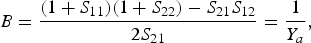 $$B = \displaystyle{\lpar 1 + S_{11}\rpar \lpar 1 + S_{22}\rpar - S_{21} S_{12} \over 2S_{21}} = \displaystyle{1 \over Y_a}\comma \;$$
 $$C = \displaystyle{1 \over Z_o} \displaystyle{\lpar 1 - S_{11}\rpar \lpar 1 - S_{22}\rpar - S_{21} S_{12} \over 2S_{21}} = 2Y_b + \displaystyle{Y_b^2 \over Y_a}\comma \;$$
 $$D = \displaystyle{\lpar 1 - S_{11}\rpar \lpar 1 + S_{22}\rpar + S_{21} S_{12} \over 2S_{21}} = 1 + \displaystyle{Y_b \over Y_a}\comma \;$$
 $$Y_a = \displaystyle{1 \over B} = \displaystyle{1 \over R_g} + jB_r\comma \;$$
 $$Y_b = \displaystyle{A - 1 \over B}=\displaystyle{ - 1 \pm \sqrt{1 + BC} \over B} = \displaystyle{D - 1 \over B} = G_p + jB_p.$$
B) Extracted circuit parameters for DGS unit cell
Now, by making use of the S- or ABCD-parameters as expressed in equations (3–8), one can estimate equivalent circuit components of the unit DGS cell as follows [Reference Kim and Lee48, Reference Haiwen, Xiaowei and Zhengfan51]:
 $$C_g = \displaystyle{B_r \over \omega _2 \left(\displaystyle{\omega_1 \over \omega_2} - \displaystyle{\omega_2 \over \omega_1} \right)}\comma \;$$
 $$L_g = \displaystyle{1 \over \omega ^2 C_g}\comma \;$$
 $$C_p = \displaystyle{B_p \over \omega_1}\comma \;$$
 $$R_g = \displaystyle{1 \over \hbox{Re} \lsqb Y_a\rsqb }\comma \;$$
 $$G_p = \hbox{Re} \lsqb Y_b\rsqb.$$
Here, ω 1,ω 2, and ω are the lower 3-dB cutoff frequency, the upper 3-dB cutoff frequency, and the operating frequency, respectively.
C) Propagation constant γ in terms of ABCD and S-parameter
Now, the propagation constant for unit DGS cell can be directly calculated from the S-parameters as [Reference Chae, Lim, Pyo, Jeon and Bae52, Reference Mao and Chen53]:
 $$\gamma = \displaystyle{1 \over d} \cosh^{ - 1} \left[\displaystyle{1 - S_{11}^2 + S_{21}^2 \over 2S_{21}} \right].$$
By using ABCD-parameters, the propagation constant can also be calculated as:
 $$\gamma = \displaystyle{1 \over d} \cosh^{ - 1} \left[\displaystyle{A + D \over 2} \right]\comma \;$$
where d is the electrical length of the microstrip line.
The given relations in equation (14) and (15) are derived using the Floquet mode theorem in lossy microstrip line when the unit DGS cell is symmetric [Reference Chae, Lim, Pyo, Jeon and Bae52, Reference Mao and Chen53].
6. SLOW WAVE EFFECT (SWF)
When a unit DGS cell is introduced into the ground plane of the microstrip line, the return path of the current is fully disturbed and this current is confined to the periphery of the perturbation along the DGS side arm. Owing to the increased path length of the current, propagation delay will occur. Hence, phase velocity is reduced. This phenomenon is called slow-wave effect. The SWF is the relation between the wave number in free space k 0 and the propagation constant β of the transmission line. For lossless microstrip line [Reference Liu, Li and Sun54, Reference Tirado Mendez, Aguilar, Gonzalez and Reyes Ayala55]:
 $$SWF = \sqrt{\varepsilon_{eff}}\comma \;$$
 $$\beta = \sqrt{\varepsilon_{eff}} k_o = \displaystyle{\omega \over v_p} = \displaystyle{\omega \over c} \sqrt{\varepsilon_{eff}}\comma \;$$
where v p is the phase velocity and ε eff is effective permittivity.
7. ADVANTAGES OF DGS IN MICROSTRIP FILTERS
Microstrip filters employed with DGS have several advantages over their conventional counterparts such as size reduction, bandwidth enhancement, harmonics suppression, and sharpness enhancement. The advantages with respect to size reduction, bandwidth enhancement, sharpness enhancement, harmonic suppressions, and coupling enhancement are discussed in the subsections of this section.
A) Size reduction techniques in microstrip filter with DGS
When a DGS unit cell is employed in a microstrip line, it is necessary to find the electrical length of microstrip line due to the DGS. Consequently, the slow-wave effect comes into picture for extended current path length. Now, for this microstrip line with DGS, electrical length is given by Liu et al. and Tirado Mendez et al. [Reference Liu, Li and Sun54, Reference Tirado Mendez, Aguilar, Gonzalez and Reyes Ayala55].
 $$\theta = \beta l = \sqrt{\varepsilon_{eff}} k_o l.$$
Here, θ is electrical length of the microstrip line, β is the propagation constant, l is the length of line, ɛ eff is effective permittivity of the microstrip line, and k o is the wave number.
As the DGS is introduced in the ground plane of the microstrip line, the effective inductance and capacitance will change and these in turn will change the resonant frequency of the microstrip line [Reference Liu, Li, Sun, Kurachi, Chen and Yoshimasu50]. For keeping the resonant frequency at its initial value, we have to compensate for the length of the transmission line. In this way, miniaturization will occur in transmission line using the DGS. This concept is formulated in the equations given below:
The input impedance of the line when there is no defect in the ground plane is shown in equation (19) [Reference Pozar56]:
 $$Z_{ino} = Z_o \left[\displaystyle{Z_l + jZ_o \tan \beta_o l_o \over Z_o + jZ_l \tan \beta_o l_o} \right]\comma \;$$
where Z o is the characteristic impedance and Z l is load impedance of the microstrip line.
After inserting defect on the ground plane in the line, equation (20) shows line impedance with DGS,
 $$Z_{ind} = Z_o \left[\displaystyle{Z_l + jZ_o \tan \beta _d l_o \over Z_o + jZ_l \tan \beta_d l_o} \right].$$
After inserting defect on the plane its resonating frequency is shifted to a new value. The impedance of the line at this resonant frequency is
 $$Z^{\prime}_{ind} = Z_o \left[\displaystyle{Z_l + jZ_o \tan \beta_d^{\prime} l_o \over Z_o + jZ_l \tan \beta_d^{\prime} l_o} \right]\left(\therefore \,Z_o = \sqrt{\displaystyle{L \over C}} \right).$$
Owing to the insertion of DGS in the ground plane, characteristic impedance of the line will also change due to change in inductance and capacitance [Reference Yang, Weng, Wu, Huang and Houng57]. In equation (21), the expression of characteristic impedance, inductance, and capacitance have been shown [Reference Yang, Weng, Wu, Huang and Houng57].
Now, a change in the electrical length can be compensated for by changing the length of the line to regain the original impedance value.
 $$Z_{indm} = Z_o \left[\displaystyle{Z_l + jZ_o \tan \beta _{dm} l_{dm} \over Z_o + jZ_l \tan \beta_{dm} l_{dm}} \right].$$
Under these conditions,
 $$Z_{ino} = Z_{indm}\comma \;$$
 $$\Rightarrow \theta_o = \theta_{dm} \Rightarrow \displaystyle{l_{dm} \over l_o} = \displaystyle{\beta_o \over \beta_{dm}} \lpar \because \beta _{dm} = \beta_d\rpar .$$
When no DGS is employed, the electrical length at a given frequency is
 $$\theta_o = \beta_o l_o = \left(\displaystyle{2\pi f_o \over c} \right)\sqrt{\varepsilon_{eff}} l_o.$$
After inserting DGS into the microstrip line, electrical length of the line will change to a value given by,
 $$\theta_d = \beta_d l_o = \left(\displaystyle{2\pi f_o \over c} \right)\sqrt{\varepsilon_{effd}} l_o.$$
From equation (25) to (26) we obtain,
 $$\displaystyle{\theta_o \over \theta_d} = \displaystyle{\beta_o \over \beta_d} = \sqrt{\displaystyle{\varepsilon_{eff} \over \varepsilon_{effd}}} = \displaystyle{SWF_o \over SWF_d}.$$
The insertion of DGS shifts the attenuation pole leftwards when compared with the simple microstrip line without DGS. Now, to reset the resonant frequency to its initial value, one has to compensate for the electrical length. Under these conditions,
 $$\theta_d^{\,\prime} = \theta_{dm}\comma \;$$
 $$\left(\displaystyle{2\pi f_d^{\prime} \over c} \right)\sqrt{\varepsilon_{effd}} l_o = \left(\displaystyle{2\pi f_o \over c} \right)\sqrt{\varepsilon_{effd}} l_{dm}.$$
Using equation (25–29), we can write equation (30) which results in the propagation constant, frequency, and length of transmission line with DGS and without DGS,
 $$\displaystyle{l_{dm} \over l_o} = \displaystyle{f_d^{\prime} \over f_o} = \displaystyle{\theta_o \over \theta_d} = \displaystyle{\beta_o \over \beta_d} = \sqrt{\displaystyle{\varepsilon_{effo} \over \varepsilon_{effd}}}.$$
Equation (31) shows the relation between SWF, phase velocity, and LC parameter with and without DGS.
 $$\displaystyle{SWF_o \over SWF_d} = \displaystyle{v_{pd} \over v_{po}} = \sqrt{\displaystyle{L_o C_o \over L_d^{\prime} C_d^{\prime}}}.$$
Using the equations (27, 30, and 31), we can write the following expression:
 $$\displaystyle{l_{dm} \over l_o} = \sqrt{\displaystyle{\varepsilon_{effo} \over \varepsilon_{effd}}} = \displaystyle{SWF_o \over SWF_d} = \sqrt{\displaystyle{L_o C_o \over L_d^{\prime} C_d^{\prime}}}.$$
Equation (32) depicts that when the product of inductance and capacitance is more with DGS as compared to line without DGS, the length of the line will reduce.
B) Bandwidth enhancement in microstrip filter with DGS
Owing to the incorporation of DGS, effective inductance and capacitance will change [Reference Liu, Li, Sun, Kurachi, Chen and Yoshimasu50]. Owing to the change of this effective inductance and capacitance, characteristic impedance will also be changed. The quality factor will also change due to change in inductance and capacitance. The quality factor can be written as:
 $$Q = \displaystyle{f_o \over BW}.$$
Here, f o is the resonating frequency, BW is the bandwidth of operating devices, and Q is the quality factor. Bandwidth without defect is
 $$BW_o = \displaystyle{f_o \over Q_o} = \displaystyle{f_o \over Z_o} \sqrt{\displaystyle{L_o \over C_o}}.$$
Here, Z o is the characteristic impedance, L o is the inductance at f o frequency, C ois the capacitance at f o frequency, and Q o is the total quality factor at resonance frequency.
When a defect is created on the ground or on the surface of the line, the new bandwidth due to shift in the resonance frequency is
 $$BW_D = \displaystyle{f_D \over Z_o} \sqrt{\displaystyle{L_d \over C_d}}.$$
After minimization, the bandwidth is again changed due to change in inductance and capacitance,
 $$BW_{dm} = \displaystyle{f_0 \over Q_{dm}} = \displaystyle{f_0 \over Z_0} \sqrt{\displaystyle{L_{dm} \over C_{dm}}}.$$
The percentage increment in the bandwidth of a compact DGS loaded structure with respect to bandwidth of conventional structure is
 $$\displaystyle{BW_{dm} - BW_0 \over BW_0} \times 100 = \left(\sqrt{\left(\displaystyle{L_{dm} \times C_0 \over C_{dm} \times L_0} \right)} - 1 \right)\times 100.$$
From equation (33), if the quality factor decreases, bandwidth will increase but circuit performance is degraded because of increased losses. Thus, there is a trade off between the value of L and C in such a manner that the performance of the filters should not degrade. The inductance and capacitance depend on the lattice dimensions and slot gap of the DGS. The percentage bandwidth of the filter with DGS can be calculated in terms of L and C as shown in equation (37).
C) Enhancement of sharpness in microstrip filter with DGS
Figure 7(a) shows the layout of five pole low-pass filter (LPF) incorporated with square dumbbell shaped DGS (DB-DGS) as well as spiral-shaped DGS (SP-DGS) [Reference Yang and Wu58]. The combination of both DB-DGS and SP-DGS improves sharpness of the filter. The sharpness of the filter depends on the length of the connecting slot that connects the square heads of DB-DGS. It is well explained in [Reference Ahn, Park, Kim, Kim, Qian and Itoh18]. If the slot length is increased, effective capacitance will also increase. Owing to the limitation of increasing the slot length in DB-DGS, the effective capacitance is less as compared to the SP-DGS.
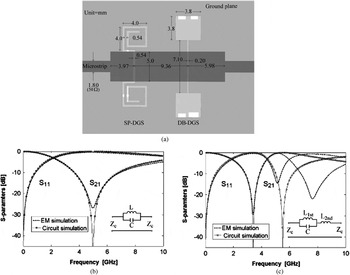
Fig. 7. Five pole LPF with simulated results (a) design configuration, (b) DB-DGS (L = 3.0619 nH, C = 0.3336 pF), and (c) SP-DGS (L 1st = 2.139999 nH, L 2nd = 1.3216 nH, and C = 1.0210 pF) [Reference Yang and Wu58].
Figures 7(b) and 7(c) show the simulated results of a five pole elliptic-function LPF using DB-DGS and SP-DGS. In Fig. 7(b), the DB-DGS has smaller capacitance and wider stopband, while the Fig. 7(c) SP-DGS shows larger capacitance and steeper stopband. Therefore, by employing both DB-DGS and SP-DGS, the characteristics of the sharp transition knee and wide stopband can be obtained [Reference Yang and Wu58]. The sharpness of the filter can be expressed as [Reference Abdel-Rahman, Verma, Boutejdar and Omar42]:
 $$SharpnessFactor =\; \displaystyle{f_{CL} \over f_o}$$
Where f CL is 3-dB lower cut-off frequency and f o is the resonance frequency.
D) Harmonics suppression and widening the rejection band in low pass/band pass filter with DGS
For suppressing the harmonics in microstrip filters, two approaches can be used. One is lumped elements such as a chip capacitor [Reference Sheen59] or a sheet resistor [Reference Lee, Ryu, Yom and Lee60] can be incorporated into the distributed line circuits in order to break their periodicity with respect to frequency [Reference Lee, Ryu, Yom and Lee60]. Another approach is to employ a PBG/EBG or DGS [Reference Yang, Qian and Itoh61]. Various techniques are used to suppress the harmonics in the microstrip filter using DGS such as stepped-impedance and shunt stubs for series L and shunt C components in the passband. A conventional DB-DGSs and stepped impedance shunt stubs (SISSs) are employed as series and shunt elements of L and C. When the conventional DB-DGSs are introduced into the ground plane of transmission line, the effective capacitance varies with the gap width of the slot connecting the dumbbell heads. The effective capacitance increases with a decrease in the slot gap thus leading to an upward shift in the resonance frequency. An increase in the dumbbell head dimension results in an increase in the effective inductance thus leading to a downward shift in the 3 dB cut-off frequency [Reference Ahn, Park, Kim, Kim, Qian and Itoh18]. By adjusting the value of L and C of the SISSs without affecting the original low-pass characteristics, the harmonics can be suppressed [Reference Park, Kim and Nam62]. For removing the second and third harmonics an asymmetric spiral DGS can be used. A single asymmetric DGS provides two different resonance frequencies because of different sizes of spiral shaped defects on the ground plane. The transfer function of the asymmetric DGS shows signal rejection characteristics at two different resonance frequencies and the characteristics of asymmetric DGS are modeled by two parallel RLC resonance circuits in cascade [Reference Woo and Lee63]. Other techniques for suppression of harmonics using DGS use inter-digital capacitance in the conducting strip line which provides a large capacitance to disturb the periodicity of the microstrip filter with DGS [Reference Qi and Liu64]. Various other techniques are also available for harmonic suppression using DGS for specific applications [Reference Sung, Kim and Kim65–Reference Park, Kim and Nam70]. The bandstop characteristics can be used in widening the rejection band in LPF and band-pass filter. To suppress the higher order harmonics, the unit DGS array can be used. Some researchers used C-shaped DGS in ground plane as well as in conducting strip to obtain a wide stopband [Reference Kumar Parui and Das71, Reference Ting, Tam and Martins72].
E) Coupling enhancement in band-pass filter using DGS
A DGS etched in the ground plane beneath the coupled lines of a parallel coupled band-pass filter enhances coupling between the lines due to slow wave effect of DGS. The SWF of a DGS increases toward the edge of the stopband. Hence, by using this property of DGS, coupling in coupled line filters can be improved. The coupling coefficient is defined by [Reference Kumar Parui and Das71]:
 $$S_{41} = \left\vert sin\lpar \pi \Delta n_{eff} Lf/c\rpar \right\vert\comma \;$$
where  $\Delta n_{eff} = \sqrt{\varepsilon_{effe}} - \sqrt{\varepsilon_{effo}}\; \Delta n_{eff} $ is the effective dielectric constant, ɛeffe is the dielectric constant for even mode, and ɛeffo is the dielectric constant for odd mode.
A wave travels a longer path in even modes due to which signals slow down and the phase velocity decreases. This leads to an increase in dielectric constant. In the odd mode, E-field pattern is asymmetric, i.e. the E-field is continuous even in the presence of DGS. Hence, the slow wave effect does not appear. Therefore, the effective dielectric constant increases with insertion of a DGS and thus the coupling coefficient is enhanced [Reference Kumar Parui and Das71]. When the DGS slots are incorporated along an electrically large distance under the feed line of parallel coupled lines, the slot must be separated from the adjacent slot to avoid slot mode propagation. If the printed metal bridges separating the slots are eliminated, the filter response will be poor [Reference Velazquez-Ahumada, Martel and Medina73].
8. DISADVANTAGES OF DGS IN MICROSTRIP FILTER
There are many disadvantages of DGS in microstrip filters but mainly two disadvantages are more prominent. One is radiation loss and the second is packaging complexity. Both the disadvantages are discussed in brief here.
A) Radiation loss in microstrip filter with DGS
Owing to radiation losses, the insertion loss increases in the passband for band-pass filters and in the rejection band for LPF. The radiation loss can have a severe effect on the system performance because of interference. To reduce these effects, the DGS structure is placed in a metallic box to improve the performance [Reference Boutejdar, Elsherbini and Omar36]. The radiation loss is also being stated in terms of radiation rate and is given in (45) and (47).
B) Radiation rate
The radiation rate is related roughly to the DGS size. If the size of DGS becomes comparable to the wavelength, it will start to function as a radiator instead of a resonator. An expression for radiation rate can be established in terms of equivalent circuit element values. A simple RLC resonator circuit of a unit DGS cell is shown in Fig. 8(a).
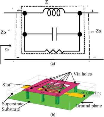
Fig. 8. (a) RLC circuit for unit DGS resonator [Reference Kim and Lee48]. (b) 3D view superstrate-substrate microstrip filter with inter-digital DGS [Reference Balalem, Machac and Omar74].
The reflection coefficient at the input side is
 $$S_{11} = \displaystyle{Z_{in} - Z_0 \over Z_{in} + Z_0} = \displaystyle{Z \over Z+2Z_o}\comma \;$$
 $$Z_{in} = Z + Z_o.$$
The voltage across Z is “V” and V + is the incident voltage.
 $$V = V_1 \displaystyle{Z \over Z + Z_o} = V^+ \displaystyle{2Z \over Z + 2Z_o}.$$
The incident power P in is given by
 $$P_{in} = \displaystyle{\left\vert V^+ \right\vert ^2 \over 2Z_o}.$$
Radiated power P r is expressed as
 $$P_r = \displaystyle{\left\vert V \right\vert^2 \over 2R} = \displaystyle{2\left\vert V^+ \right\vert^2 \left\vert \displaystyle{Z \over Z + 2Z_o} \right\vert^2 \over R}.$$
The radiation rate is defined as
 $$\eta = \displaystyle{P_r \over P_{in}} = \displaystyle{2\left\vert V^+ \right\vert^2 \left\vert \displaystyle{Z \over Z+2Z_o} \right\vert ^2 \over R} \times \displaystyle{2Z_o \over \left\vert V^+ \right\vert^2} = 4\left\vert \displaystyle{Z \over Z + 2Z_o} \right\vert^2 \displaystyle{Z_o \over R}.$$
At the resonant frequency (ω → ωo), (Z → R), η can be
 $$\eta \left(\displaystyle{R \over Z_o} \right)= \displaystyle{1 \over \displaystyle{R \over 4Z_o} + \displaystyle{Z_o \over R} + 1}.$$
As a function of R/Z o, η can be shown to have its maximum value of 0.5 when R/Z o = 2. The radiation rate or radiation efficiency can also be expressed in S-parameters as shown in equation (47)
 $$\eta = 1 - \left\vert S_{11} \right\vert^2 - \left\vert S_{21} \right\vert^2.$$
C) Packaging complexity
Generally, DGS structures are designed by opening a circuit to enhance its performance as well as size reduction of the circuit. Such structures increase packaging complexity. To remove packaging complexity, an additional superstrate–substrate is placed on top of the substrate and the original ground plane of the circuit is left fully metalized. The ground plane of the substrate is connected with metal on the superstrate via holes and defect is created in this top layer as shown in Fig. 8(b). This structure has higher quality factor than that for the classical DGS Structure [Reference Balalem, Machac and Omar74].
9. MODELING OF MICROSTRIP FILTER WITH DGS USING SOFT COMPUTING TECHNIQUES
There is no direct correlation between the physical dimensions of the DGS and equivalent LC parameters. Artificial neural network (ANN) techniques such as sampling ANN model, a radial basis function neural network (RBFNN), and back wave propagation are available for modeling of DB-DGS [Reference Wang, Jiang, Gao, Wang and Liu75]. Here, by using the sampling function, the ANN model of a DGS is shown in Fig. 9. The value of L and C can be obtained easily without any need to simulate. A DB-DGS etched on the ground plane of a conventional 50 Ω microstrip transmission line with a dielectric constant of 10.5 and a thickness of 50 mil are considered. In the neural network model of the dumbbell DGS, the input variables are the dimensions of the DGS dimensions and the outputs of the ANN model are 3-dB cut-off (f c) and resonance frequency (f o). A three layer SF-ANN is considered in which the hidden layer has 50 neurons. In the training process, 50 samples were used. Both the simulation and measured results for such structures are shown in [Reference Haiwen, Xiaowei and Zhengfan51, Reference Hamid Reza; and Khalilpour76].

Fig. 9. ANN model for DB-DGS [Reference Hamid Reza; and Khalilpour76].
10. ADDITIONAL APPLICATIONS OF DGS
The DGS techniques play key roles in reducing the size of the component, suppressing the harmonics, and enhancing the bandwidth of various microwave components such as tuneable filters [Reference Zulkifli, Rahardjo and Hartanto35, Reference Huynen, Gogilo, Vanhoenacker and Vander Vorst77], power divider [Reference Lim, Lee, Kim, Park, Ahn and Nam78], amplifiers [Reference Lim, Kim, Park, Ahn and Nam79, Reference Lim, Park, Lee, Ahn and Nam80], oscillators [Reference Lee, Lim, Park, Ahn and Nam81], frequency Doubler [Reference Jeong and Lim82], directional coupler [Reference Kim83], dual-band filters [Reference Ho, Pang and Tam84–Reference Liu87], ultra wideband (UWB)-pass filters [Reference El. Shaarawy, Coccetti, Plana, El.Said and Hashish88–Reference Lee and Kim92], and tri-band filters [Reference Ren93, Reference Liu, Dou and Zhao94]. A lot of investigations have been carried out on DGS techniques for reducing the size of the filters [Reference Liu, Li, Sun, Kurachi, Chen and Yoshimasu50, Reference Liu, Li and Sun54, Reference Chung, Jeon, Kim, Ahn, Choi and Itoh95–Reference Byun, Ko, Lee, Park and Kim108].
Antenna – The filtering characteristics of DGS can be employed in antennas for reducing the size of the antenna, mutual coupling between antenna array elements, cross polarization reductions, harmonic reductions, broadband radar cross section (RCS) reductions, and elimination of scan blindness in antenna array [Reference Breed109].
Delay lines – DGS resonators along a microstrip line introduce changes in the propagation of the wave along the line. The DGS elements slow the even mode which must propagate around the edges of the DGS slot but do not affect the odd mode transmission. With change in phase velocity, the structure is called slow wave structure which is used in delay lines [Reference Breed109].
Power divider and Couplers– The DGS structure not only achieved size reduction but also reduced harmonic signal in power divider and coupler. A 4:1 power divider was designed using conventional Wilkinson topology with DGS [Reference Lee, Lim, Park, Ahn and Nam81]. The line with DGS was enabled to realize a 150 Ω microstrip line. It has been impractical to fabricate a 4:1 power divider using conventional microstrip line because of thin conductor width and low W/H ratio. The researchers claimed that the aspect ratio (W/H) increased to 235% and the length of quarter wavelength line reduced to 83%. A periodic DGS structure was designed to implement 10 dB, 90° branch line coupler [Reference Lim, Kim, Park, Ahn and Nam110]. The researchers achieved five times miniaturization of conductor widths with DGS when compared with the conventional one. A compact microstrip rat-race hybrid coupler was designed by Sung et al. in [Reference Sung, Kim, Ahn and Kim67].
Amplifiers – Two amplifiers, one with conventional microstrip and the other with DGS were reported in [Reference Lim, Park, Lee, Ahn and Nam80]. They compared the measured performances of these two amplifiers. The measured performance of the amplifier with DGS was similar to the conventional amplifier with size reduction of 53.8% of the series microstrip lines and 55.6% of the input and output matching network. In [Reference Jeong, Jeong, Lim and Nam66], Jeong et al. proposed a quarter wavelength high impedance bias line using DGS which reduces the third harmonics by about 26.5 dB than the conventional one.
Oscillators – Microwave oscillator with DGS was first designed by Jung et al. in [Reference Jung, Park, Lim and Cho111]. The second harmonics was reduced and an increment of 1–5% in output power was achieved.
11. CONCLUSIONS
This paper gives a review of microstrip filters with DGS for beginners, who need a comprehensive overview of the subject with useful formulas to start a first-hand design. During this course, a brief introduction of DGS followed by the advantages of DGS over complex EBG/PBG structures is presented. Modeling aspects and useful equivalent circuit parameters of DGS are given for a quick start of the subject. Major advantages and limited disadvantages of DGS are enumerated. Modeling of DGS using soft computing techniques is discussed and the work concludes with various applications of DGS for a variety of design problems (from antenna to components). This study concludes giving a generalized insight that DGS plays an important role in enhancement of various performance indexes with a simple/attractive solution to an otherwise complex problem in microwave/millimeter wave domain.
 Arjun Kumar was born in Bareilly (Uttar Pradesh), India, in 1983. He received B.Tech. degree in Electronics and Communication Engineering from U.P. Technical University, Lucknow, India, in 2004 and M.Tech. degree in Microwave and Mobile Communication from Graphic Era University, Dehradun, India, in 2010. He is currently working toward the Ph.D. degree in Electronics and Communication Engineering at Indian Institute of Technology Roorkee, Roorkee, India. His current research interests include microwave planar passive components using defected ground structure and metamaterials.
 M.V. Kartikeyan was born in Nellore (Andhra Pradesh), India, in 1961. He received the M.Sc. degree in physics and Ph.D. degree in electronics engineering from Banaras Hindu University, Varanasi, India, in 1985 and 1992, respectively. He was with the Institute for Pulsed Power and Microwave Technology (IHM), Research Center (FZK), Karlsruhe, Germany. He is currently a Professor and the head of the Department of Electronics and Communication Engineering, Indian Institute of Technology, Roorkee, India. His research interests includes millimeter wave engineering (electron cyclotron masers and other high power devices and components), microstrip antennas for communications, computational electromagnetics, microwave integrated circuits, and RF & Microwave designs with soft computing techniques. Dr Kartikeyan is a Life Fellow of the Institution of Electronics and Telecommunication Engineers (IETE), Fellow of Institution of Engineers (IE) India, and senior member IEEE. He was the recipient of a Hildegard Maier Research Fellowship for Electrical Sciences presented by the Alexander von Humboldt Foundation (December 1998 to January 2000) and the Alexander von Humboldt Research Fellowship for long-term cooperation (July 2001 to June 2003).


