I. INTRODUCTION
Microstrip antenna has been considered as a good choice for compact communication devices due to their attractive advantages such as small size, low cost, light weight, low profile, ease of fabrication, integrable capability with other devices. The main limitations of the microstrip antenna are narrow impedance bandwidth and single operating frequency characteristics [Reference Lo, Solomon and Richards1, Reference Garg, Bhartia, Bahl and Ittipiboon2]. With the increase in demand of wireless applications now-a-days there is a need of diverse antennas operating in different frequency bands [Reference Vaughan and Andersen3]. These antennas when integrated on a single chip make the device bulky and costly. Thus, the solution is to design a single antenna with operation in different frequency bands with wideband radiation characteristics. Several techniques using stacked elements have been proposed in the previous years for dual band but with linear polarization [Reference Anguera, Puente, Borja, Delbene and Soler4, Reference Falade, Gao, Chen and Parini5]. A number of designs have been presented in the earlier years for increasing the versatility and bandwidth of the antenna using multilayer stacking, parasitic coupling, slot loading, tuning, and device loading [Reference Kumar, Kanaujia, Khandelwal and Gautam6–Reference Gupta, Kanaujia and Pandey8].
The S and C bands are most widely used bands for mobile satellite to earth communication. For the emerging space telecommunication, need of circularly polarized antenna arises as multipath interference is present [Reference Elbert9, Reference Skriverik, Zurcher, Staub and Mosig10]. Polarization diversity combats multipath fading [Reference Kajiwara11]. Circularly polarized antennas are extensively employed in modern communication systems such as global positioning system (GPS), wireless local area network (WLAN), radio frequency identification (RFID) readers, etc. due to their ability to provide better mobility, high link reliability, weather penetration capability, and spectral efficiency [Reference Godara12]. Over the years, several designs of circularly polarized antennas have been provided. Circularly polarized antenna can be either single feed or dual feed. In dual feed, a 90° phase shift is present between the feeds. However, single-feed antennas are more preferred due to their less cost, simplicity, and compactness as they do not require separate feed network. A single-feed square patch with truncated corners on the opposite side and rectangular slotted patch antenna has been reported [Reference Sharma and Gupta13, Reference Gautam, Benjwal and Kanaujia14]. The rectangular slot in the diagonal of patch makes a difference in the path length of two diagonals thus creating a difference in the resonance frequencies. Circular polarization also has been reported for circular and triangular geometries by truncating corners, introducing slit, stub, or slot in the patch [Reference Wong15–Reference Karmakar and Bialkowski17]. This not only makes the antenna circularly polarized but also reduces the size of the patch thus achieving a compact shape antenna. Several asymmetric slotted structures placed along the diagonal axis have been reported in the literature for achieving a good miniaturization [Reference Nasimuddin, Chen and Qing18].
This paper is organized into two parts. In the first part, a novel compact circularly polarized square microstrip patch with truncated corners and circular slot loaded at the center is presented. The corners are truncated using quarter part of a circle from the square microstrip patch. In the second part, a compact single-feed stacked arrangement of circular polarized microstrip antenna is presented. The circular slot loaded square microstrip patch with truncated corners is stacked with a simple circular microstrip configuration. The dual band is achieved with wide impedance bandwidth. The proposed structures are simulated and optimized using finite element method based simulator Ansoft HFSS v.14 [19]. The antenna is fabricated and measured results are in match with the simulated results.
II. ANTENNA STRUCTURE AND DESIGN
A) Compact circularly polarized microstrip antenna
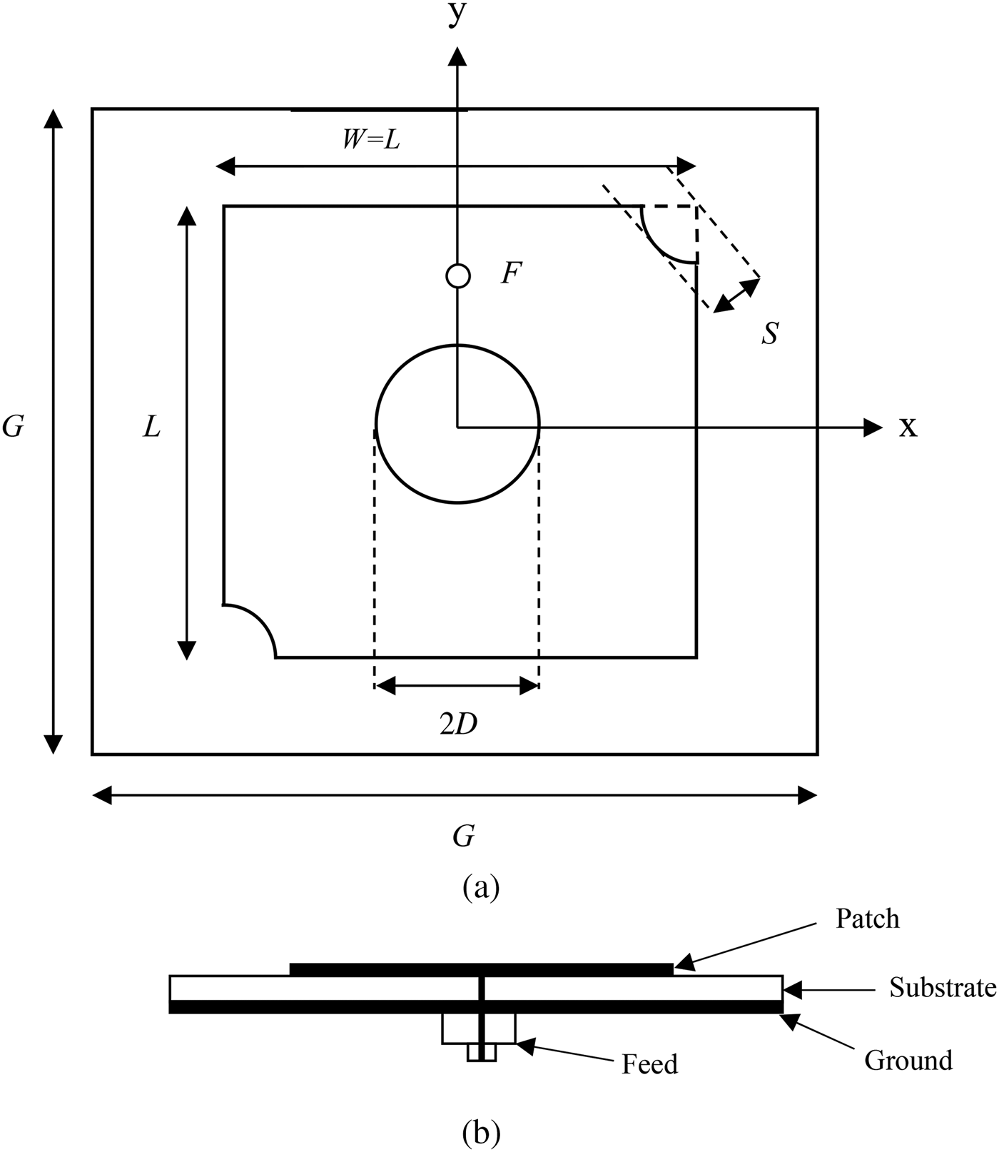
The schematic of the proposed novel compact antenna is shown in Fig. 1. The dimensions of square patch is calculated as [Reference Balanis20]
 $$L = \displaystyle{{\lambda _{eff} } \over 2}\! \comma \; $$
and
 $$\lambda _{eff} = \displaystyle{c \over {f\sqrt {\epsilon _{eff} } }}.$$

Fig. 1. Geometry of single-feed circularly polarized square microstrip antenna (a) top view (b) cross-sectional view.
Here, f is the designing frequency of the conventional square patch and ε eff is the effective dielectric constant of the structure and is defined as
 $$\epsilon _{eff} = \displaystyle{{\epsilon _{r} + 1} \over 2} + \displaystyle{{\epsilon_{r} - 1} \over 2}\displaystyle{1 \over {\sqrt {1 + 12h/W} }}\comma \; $$
h is the thickness of substrate and W is the width of the patch. In the case of square patch, the width W is chosen same as length L of the patch.
The diagonal corners of the square patch are truncated with a quarter part of a circle of radius S. Further, a circular slot of radius D is loaded at the center of the square patch. Thus the proposed compact antenna is circularly polarized. The antenna shows resonance at 2.25 GHz and compactness of around 16% is achieved in comparison with conventional square patch antenna [Reference Sharma and Gupta13]. Design specifications of the proposed antenna are provided in Table 1. The antenna is fed using 50 Ω SMA connector placed along the y-axis of the patch. The sense of rotation can be changed by simply changing the position of feed along another axis of the square patch. The ground plane considered is also a square of length G. Figure 3(a) shows the prototype of the fabricated patch.
Table 1. Dimensions of the proposed structure.

B) Circularly polarized stacked microstrip antenna for dual-band
The cross-sectional view of stacked antenna configuration is shown in Fig. 2. The circular slot loaded square microstrip patch with truncated corners is used as a driven lower patch and a top circular patch as upper parasitic element excited by fringing field of the lower patch. The radius A of upper circular patch is calculated as [Reference Balanis20]
 $$A = \displaystyle{F \over {\lcub 1 + \lpar H/50\pi \epsilon _r F\rpar [\ln \lpar 50\pi F/H\rpar + 1.7726] \rcub ^{1/2} }}.$$
Here
 $$F = \displaystyle{{8.791 \times 10^{9} } \over {f_d \sqrt {\epsilon _r } }}$$
f d is the designing frequency of the upper patch as in the case of conventional circular microstrip patch antenna with substrate height H.
 $$H = h + h_1\comma \; $$
h 1 is the thickness of upper substrate. Both the patches are fabricated on 1.6 mm thick FR-4 epoxy substrate of relative permittivity 4.4 and loss tangent of 0.0012. The photograph of the fabricated stacked antenna prototype is depicted in Fig. 3(b).

Fig. 2. Cross-sectional view of single-feed stacked microstrip antenna.

Fig. 3. Prototype of the fabricated antennas (a) compact circularly polarized square microstrip patch (b) circularly polarized stacked microstrip structure.
III. RESULTS AND DISCUSSION
When the circular slot is not integrated in the center of the square patch and diagonally corners of square patch are truncated with a quarter of a circle of radius S, the structure shows resonance at 2.45 GHz with circular polarization characteristics. The S 11 level below −10 dB is ranging from 2.38 to 2.52 GHz. The resonant frequency of the truncated square patch decreases with increase in the radius of truncated circular corner. The S 11 variation with frequency for different values of radius of truncated circular corner of radius S is shown in Fig. 4. The variation of axial ratio with frequency for different values of radius S of truncated circular corner is shown in Fig. 5. Axial ratio band ranging from 2.43 to 2.50 GHz is observed with different values of radius S. By truncating the corners of the proposed structure, the antenna shows circular polarization behavior.

Fig. 4. Variation of S 11 (dB) with frequency (GHz) for different S without circular slot loaded in the center.

Fig. 5. Variation of axial ratio (dB) with frequency (GHz) for different S without circular slot loaded in the center.
By integrating a circular slot in the center of the truncated square patch, the compactness is improved and resonant frequency is shifted at 2.25 GHz because the path of the surface current is increased. The impedance bandwidth below −10 dB lies in the range from 2.19 to 2.32 GHz. The variation of S 11 with frequency of circular slot loaded square patch antenna with truncated corners is shown in Fig. 6. The proposed prototype is fabricated using standard photolithography process. 50 Ω SMA connector is used to fed the fabricated antenna. The electrical characteristic of the fabricated antenna is measured on Agilent Network Analyzer (PNA L-Series). The return loss level at the resonating frequency is about 21 dB. The return loss level of fabricated antenna is about 17 dB at the same resonating frequency. This acceptable difference in return loss level is considered due to fabrication losses. The variation of axial ratio with frequency is shown in Fig. 7. The axial ratio level is below 3 dB at resonate frequency ranging from 2.23 to 2.27 GHz.

Fig. 6. Variation of S 11 (dB) with frequency (GHz) for circularly polarized circular slot loaded square microstrip antenna.

Fig. 7. Variation of axial ratio (dB) with frequency (GHz) for circularly polarized circular slot loaded square microstrip antenna.
The S 11 variation with frequency for different values of radius D of circular slot integrated at the center of the truncated square patch is shown in Fig. 8. The resonant frequency of the antenna decreases with increasing the radius of center loaded circular slot. The axial ratio variation with frequency for different values of radius of circular slot is shown in Fig. 9. To fabricate the antenna the optimized values of radius of circular truncated corner and radius of circular loaded slot are chosen as 3.25 and 5 mm, respectively. The measured results of the fabricated antenna are in good match with simulated shown in Figs 6 and 7.

Fig. 8. Variation of S 11 (dB) with frequency (GHz) of truncated corner square patch for different radius of center loaded circular slot.

Fig. 9. Variation of axial ratio (dB) with frequency (GHz) of truncated corner square patch for different radius of center loaded circular slot.
A dual-band characteristic is achieved by stacking the truncated corners circular slot loaded square patch with conventional circular microstrip antenna. The variation of S 11 with frequency of stacked antenna is shown in Fig. 10. The first resonance occurs at 2.25 GHz and second resonance occurs in between 4.4 to 5.5 GHz thus a wide bandwidth of about 1 GHz is achieved with circular polarization behavior at the two frequencies. The proposed stacked antenna has a good axial ratio at both bands thus producing circular polarization characteristics. The variation of axial ratio with frequency of proposed stacked antenna is shown in Fig. 11. Circular polarization is achieved at three frequencies 2.25, 5.1, and 5.4 GHz within the operating frequency band.

Fig. 10. Variation of S 11 (dB) with frequency (GHz) for circularly polarized stacked microstrip antenna.
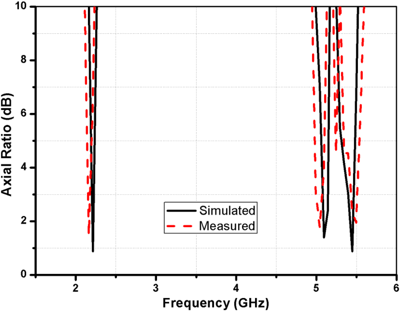
Fig. 11. Variation of axial ratio (dB) with frequency (GHz) for circularly polarized stacked microstrip antenna.
The proposed antenna shows good directivity behavior at both the operating bands. The variation of simulated directivity with frequency of stacked antenna is shown in Fig. 12. The directivity is calculated about 7 dBi at first resonance and about 8.5 dBi at second resonance. Figure 13 shows the simulated radiation efficiency of the proposed circularly polarized stacked antenna design. The E- and H-plane radiation patterns at 2.25, 5.1 and 5.4 GHz of the circularly polarized stacked antenna are shown in Fig. 14. The simulated current distribution of the proposed antenna for lower and upper patches at 2.25 GHz is shown in Fig. 15.

Fig. 12. Variation of simulated directivity (dBi) with frequency (GHz) for circularly polarized stacked microstrip antenna.

Fig. 13. Variation of simulated radiation efficiency (%) with frequency (GHz) for circularly polarized stacked microstrip antenna.

Fig. 14. Radiation pattern of the circularly polarized stacked microstrip antenna (a) 2.25 GHz, (b) 5.1 GHz, (c) 5.4 GHz.

Fig. 15. Current distribution of the proposed antenna at 2.25 GHz (a) lower patch (b) upper patch.
IV. CONCLUSION
A compact circularly polarized microstrip antenna and circularly polarized stacked microstrip antenna has been designed and fabricated. The measured results are found in good agreement with the simulated. The small difference is due to fabrication tolerance, soldering of SMA connector and placement of the upper patch. Both antennas show a stable radiation characteristic with good amount of circular polarization. Stacking provides dual-band characteristics with second band covering about 1 GHz frequency range with circular polarization at two frequencies. The proposed configuration may be a good choice for circularly polarized wireless applications in comparison with the existing dual-band antennas which are mostly linearly polarized in operation.
ACKNOWLEDGEMENTS
The authors gratefully acknowledge the support provided by the Department of Science and Technology, Government of India for the project under SERC scheme project sanction order no. SR/S3/EECE/0117/2010(G).
 Sachin Kumar received his B.Tech. degree in Electronics and Communication Engineering in 2009 and M.Tech. degree in Digital Communication in 2011 from Ambedkar Institute of Technology, Delhi, India. He has published about 11 research papers in referred international journals and conferences. His research interest includes circularly polarized microstrip antennas, ultrawideband antennas, defected ground structure, and microwave components.
 Abhishek Sharma received his B.Tech. degree from Shri Mata Vaishno Devi Univesrity, Jammu, India in Electronics and Communication Engineering in 2010. He received his M.Tech. degree from Ambedkar Institute of Advanced Communication Technologies and Research, Delhi, India in RF and Microwave Engineering in 2013. His research interest includes microstrip antenna, dielectric resonator antenna, meta-materials, and computational electromagnetics.
 Binod Kumar Kanaujia is working as Associate Professor in the Department of Electronics and Communication Engineering in Ambedkar Institute of Advanced Communication Technologies and Research (formerly Ambedkar Institute of Technology), Geeta Colony, Delhi. Dr. Kanaujia joined this institute as an Assistant Professor in 2008 through selection by Union Public Service Commission, New Delhi, India and served in various key portfolios, i.e. Head of Department, In-charge Central Library, Head of Office, etc. Before joining this institute he had served in the M.J.P. Rohilkhand University, Bareilly, India as Reader in the Department of Electronics and Communication Engineering and also as the Head of the Department. He has been an active member of Academic Council and Executive Council of the M.J.P. Rohilkhand University and played a vital role in academic reforms. Prior, to his career in academics, he had worked as Executive Engineer in the Research and Development division of M/s UPTRON India Ltd. He completed his B.Tech. in Electronics Engineering from KNIT Sultanpur, India in 1994. He did his M.Tech. and Ph.D. in 1998 and 2004; respectively, from the Department of Electronics Engineering, Indian Institute of Technology, Banaras Hindu University, Varanasi, India. He has been awarded Junior Research Fellowship by UGC Delhi in the year 2001–2002 for his outstanding work in electronics field. He has keen research interest in design and modeling of microstrip antenna, dielectric resonator antenna, left-handed metamaterial microstrip antenna, shorted microstrip antenna, ultra wideband antennas, and reconfigurable and circularly polarized antenna for wireless communication. He has been credited to publish more than 105 research papers with more than 200 citations with h-index of 10 in peer-reviewed journals and conferences. He has supervised 45 M.Tech. and three Ph.D. research scholars in the field of Microwave Engineering. He is a reviewer of several journals of international repute, i.e. IET Microwaves, Antennas and Propagation, IEEE Antennas and Wireless Propagation Letters, Wireless Personal Communications, Journal of Electromagnetic Wave and Application, Indian Journal of Radio and Space Physics, IETE Technical Review, International Journal of Electronics, International Journal of Engineering Science, IEEE Transactions on Antennas and Propagation, AEU-International Journal of Electronics and Communication, International Journal of Microwave and Wireless Technologies, etc. He has successfully executed four research projects sponsored by several agencies of Government of India, i.e. DRDO, DST, AICTE, and ISRO. He is also a member of several academic and professional bodies, i.e. IEEE, Institution of Engineers (India), Indian Society for Technical Education and The Institute of Electronics and Telecommunication Engineers of India.
 Mukesh Kumar Khandelwal received his B.Tech. degree in Electronics & Communication Engineering in 2010 and M.Tech. degree in Digital Communication in 2012 from GGSIP University, Delhi, India. He has published 11 research papers in referred international journals and conferences. His current research interests focus on microstrip antennas, defected ground structure, and microwave components.
 Anil Kumar Gautam received his B.E. degree in Electronics and Communication Engineering from Kumaon Engineering College, Almora, India and Ph.D. degree in Electronics Engineering from Indian Institute of Technology Banaras Hindu University, Varanasi, India in 1999 and 2007, respectively. Currently, Dr., Gautam is working as Associate Professor in G.B. Pant Engineering College, Uttrakhand, India. He is the author/coauthor of more than 60 research papers published in refereed international journals and conferences. He is the author of 12 books in the field of Electronics Engineering. His main research interests are microstrip antennas, ultrawide bandwidth antennas, and reconfigurable antennas.